background image

MATSUI  2107 NS

Recommended Safety Parts

Item

Part No.

Description

R401

R3K181102J

R,METAL

1K OHM 1W

R408

R6558A4R7J

R,FUSE

4.7 OHM 2W

R423

R65582680J

R,FUSE

68 OHM 1/2W

R424

R5X2CE5R6J

R,CEMENT

5.6 OHM 7W

R426

R6358A010J

R,FUSE

1 OHM 2W

R429

R655811R8J

R,FUSE

1.8 OHM 1W

R503

R5Y4AE5R6J

R,CEMENT

5.6 OHM 7W

R512

R61584470J

R,FUSE

47 OHM 1/4W

R513

R3X28B683J

R.METAL

68K OHM 3W

R516

R3X28B150J

R,METAL OXIDE

15 OHM 3W

R524

R5X2CD010J

R,CEMENT

1 OHM 5W

R804

R3U18A153J

R,METAL

15K OHM 2W

R806

R3U18A153J

R,METAL

15K OHM 2W

R808

R3U18A153J

R,METAL

15K OHM 2W

C501

P2222B224K

CMP

0.22 UF 250V AC MMCA

C502

CB3930MH3M

CC

0.0022UF 250V

C525

CB3930M12K

CC

100 PF 250V

C526

P2222B224K

CMP

0.22 UF 250V AC MMCA

C527

CB3930M12K

CC

100 PF 250V

D404

D28T10ELS6

DIODE,RECTIFIER

10ELS6TA1B2

D407

D28T10ELS6

DIODE,RECTIFIER

10ELS6TA1B2

D501

D2BTRM11C0

DIODE,RECTIFIER

RM11C

D502

D2BTRM11C0

DIODE,RECTIFIER

RM11C

D503

D2BTRM11C0

DIODE,RECTIFIER

RM11C

D504

D2BTRM11C0

DIODE,RECTIFIER

RM11C

D510

D28I15DF60

DIODE,SILICON

15DF6-FC

D511

D28T10ELS6

DIODE,RECTIFIER

10ELS6TA1B2

D515

D28F30DF60

DIODE,RECTIFIER

30DF6-FC

IC201

I03DE68120

IC

LA76812

IC401

I03SD78400

IC

LA7840

IC402

I07B9805T0

IC

BA17805T

IC403

I07B9809T0

IC

BA17809T

IC501

IDED016846

IC

TDA16846

IC502

I07B9805T0

IC

BA17805T

Q401

TC4Q052500

TRANSISTOR,SILICON

2SC5250

Q501

T41F026510

TRANSISTOR FIELD EFFECT

2SK2651-01MR

Q503

TA3T1371A0

TRANSISTOR,SILICON

2SA1371(D,E)-AE

Q504

TC30041600

TRANSISTOR,SILICON

2SC4160-ORI

L502

029K000001

COIL,LINE FILTER

RB-20871

T501

048140049W

TRANSFORMER SWITCHING

8140049W

J801

066C130015

SOCKET,CATHODE RAY TUBE

CVT3275-5102

SW501

0530205002

SWITCH

SDDFC30400

CD501

1206635821

CORD,AC

1206635821

F501

0808T04002

FUSE

218004

F502

0808T01002

FUSE

218001.

FB401

043221010F

TRANSFORMER,FLYBACK

3221010

ICP501

083PC02002

MICRO FUSE

251002

RY501

0560Q10114

RELAY

SDT-SS-109DM

V801

098A210405

CRT

A51EER131*76

(2107R & 2107T Only)
R429

R655811R5J

R, FUSE

1.5 OHM 1W

R448

R5Y4CD472J

R, CEMENT

4.7K OHM 5W

R514

R3X28B683J

R, METAL

68K OHM 3W

R518

R3X18A220J

R, METAL OXIDE

22 OHM 2W

R524

R5X2CD1R8J

R, CEMENT

1.8 OHM 5W

L501

029X000073

COIL, LINE FILTER

SS24H-07200

T501

048140051W

TRANSFORMER, SWITCHING

8140051W

Safety Precautions

PERFORM A SAFETY CHECK AFTER
SERVICING
Confirm that the screws, parts and wiring which
were removed in order to service are put in the
original positions, or whether there are the
portions which are deteriorated around the
serviced places serviced or not. Check the
insulation between the antenna terminal or
external metal and the AC cord plug blades.
And be sure the safety of that.

(INSULATION CHECK PROCEDURE)
1. Unplug the plug from the AC outlet.
2. Remove the antenna terminal on TV and turn

on the TV.

3. Insulation resistance between the cord plug

terminals and the eternal exposure metal
[Note 2] should be more than 1M ohm by
using the 500V insulation resistance meter
[Note 1].

4. If the insulation resistance is less than 1M

ohm, the inspection repair should be required.

[Note 1]
If you have not the 500V insulation resistance
meter, use a Tester.

[Note 2]
External exposure metal:Antenna terminal

Disassembly Instructions

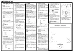
1. REMOVAL OF ANODE CAP

Read the following NOTED items before starting
work.

*  After turning the power off there might still be

a potential voltage that is very dangerous.
When removing the Anode Cap, make sure to
discharge the Anode Cap’s potential voltage.

*  Do not use pliers to loosen or tighten the

Anode Cap terminal, this may cause the
spring to be damaged.

REMOVAL
1. Follow the steps as follows to discharge the

Anode Cap. (Refer to Fig. 1-1.) Connect one
end of an Alligator Clip to the metal part of a
flat-blade screwdriver and the other end to
ground. While holding the plastic part of the
insulated screwdriver, touch the support of the
Anode with the tip of the screwdriver.
A cracking noise will be heard as the voltage
is discharged.

2. Flip up the sides of the Rubber Cap in the

direction of the arrow and remove one side of
the support. (Refer to Fig. 1-2.)

3. After one side is removed, pull in the opposite

direction to remove the other.

NOTE
Take care not to damage the Rubber Cap.

INSTALLATION
1. Clean the spot where the cap was located

with a small amount of alcohol. (Refer to Fig.
1-3.)

NOTE
Confirm that there is no dirt, dust, etc. at the
spot where the cap was located.

2. Arrange the wire of the Anode Cap and make

sure the wire is not twisted.

3.Turn over the Rubber Cap. (Refer to Fig. 1-4.)

4. Insert one end of the Anode Support into the

anode button, then the other as shown in Fig.
1-5.

5. Confirm that the Support is securely con-

nected.

6. Put on the Rubber Cap without moving any

parts.

Service Mode List
This unit provided with the following SERVICE
MODES so you can repair, examine and adjust
easily.
To enter the Service Mode, press both set key
and remote control key for more than 2 seconds.

CONFIRMATION OF USING HOURS
POWER ON total hours can be checked on the
screen. Total hours are displayed in 16 system
of notation.
1. Set the VOLUME to minimum.
2. Press both VOL. DOWN button on the set and

Channel button (6) on the remote control for
more than 2 seconds.

3. After the confirmation of using hours, turn off

the power.

NOTE FOR THE REPLACING OF MEMORY IC
If a service repair is undertaken where it has
been required to change the MEMORY IC, the
following steps should be taken to
ensure correct data settings while making
reference to TABLE 1.

Table 1 (2107 NS Only)

NOTE: No need for the setting after INI 10.

Table 1 (2107 R Only)

NOTE: No need for the setting after INI 16

Table 1 (2107 T Only)

NOTE: No need for the setting after INI 10

1. Enter DATA SET mode by setting VOLUME to

minimum.

2. Press both VOL. DOWN button on the set

and Channel button (6) on the remote control
for more than 2 seconds.

3. ADDRESS and DATA should appear as Fig 1.
4. ADDRESS is now selected and should

“blink”. Using the SET + or - keys on the
remote, step through the ADDRESS until
required ADDRESS to be changed is
reached.

5. Press ENTER to select DATA. When DATA is

selected, it will “blink”.

6. Again, step through the DATA using SET + or

- until required DATA value has been se-
lected.

7. Pressing ENTER will take you back to

ADDRESS for further selection if necessary.

8. Repeat steps 4 to 7 until all data has been

checked.

9. When satisfied correct DATA has been

entered, turn POWER off (return to STANDBY
MODE) to finish DATA input.

The unit will now have the correct DATA for the
new MEMORY IC.

Electrical Adjustments

1. BEFORE MAKING ELECTRICAL ADJUST-

MENTS

Read and perform these adjustments when
repairing the circuits or replacing electrical parts
or PCB assemblies.

CAUTION

1-1:Prepare the following measurement tools

for electrical adjustments.

1. Synchro Scope
2. Digital Voltmeter
3. Color Bar Generator

2. BASIC ADJUSTMENTS

On-Screen Display Adjustment
In the condition of NO indication on the screen.
Press both VOL. DOWN button on the set and
the Channel button (9) on the remote control for
more than 2 seconds to appear the adjustment
mode on the screen as shown in Fig. 2-1.

NOTE
Use the Channel buttons (1-8) on the remote
control to select the options shown in Fig. 2-1.
Press the Channel button (0) on the remote
control to end the adjustments.

•  Use an isolation transformer when performing

any service on this chassis.

•  Before removing the anode cap, discharge

electricity because it contains high voltage.

•  When removing a PCB or related component,

after unfastening or changing a wire, be sure
to put the wire back in its original position.
Inferior silicon grease can damage IC’s and
transistors.

•  When replacing IC’s and transistors, use only

specified silicon grease (YG6260M). Remove
all old silicon before applying new silicon.

2-1: RF AGC DELAY

1. Receive an 80dB monoscope pattern.
2. Connect the digital voltmeter between the pin

5 of CP101 and the pin 1 (GND) of CP101.

3. Activate the adjustment mode display of Fig.

2-1 and press the channel button (5) on the
remote control.

4. Press the channel button (2) on the remote

control. The Fig. 2-2 appears on the display.

5. Press the VOL. UP/DOWN button on the

remote control until the digital voltmeter is
2.20 

±

 0.05V.

General Information

Also Covers

Matsui 2107R & 2107T.

Summary of Contents for 2107 NS

Page 1: ...ve one side of the support Refer to Fig 1 2 3 After one side is removed pull in the opposite direction to remove the other NOTE Take care not to damage the Rubber Cap INSTALLATION 1 Clean the spot where the cap was located with a small amount of alcohol Refer to Fig 1 3 NOTE Confirm that there is no dirt dust etc at the spot where the cap was located 2 Arrange the wire of the Anode Cap and make su...

Page 2: ...ess the VOL UP DOWN button on the remote control until the SHIFT quantity of the OVER SCAN on right and left becomes minimum 2 13 VERTICAL POSITION 1 Receive the monoscope pattern 2 Using the remote control set the brightness and contrast to normal position 3 Activate the adjustment mode display of Fig 2 1 and press the channel button 1 on the remote control The Fig 2 6 appears on the display 4 Pr...

Page 3: ...SURED WITH THE DIGITAL TESTER WHEN THE COLOR BROADCAST WAS RECEIVED IN GOOD CONDITION AND PICTURE IS NORMAL NOTE B101 BLM21A601SPT OF PRINTING AND SUBJECT TO CHANGE WITHOUT NOTICE NOTE THIS SCHEMATIC DIAGRAM IS THE LATEST AT THE TIME BT001 R03 AB E_20_T BT002 R03 AB E_20_T TM101 SBER00179A CP101 8283_0912_00_000 1 2 3 4 5 6 7 8 9 S802Y Q103 DTC114TKA AV SW CAUTION DIGITAL TRANSISTOR FBT_5V VD TUNE...

Page 4: ...47 50V KS C609 0 1 50V KS C319 100 10V YK C314 1 50V YK C313 1 50V KS C321 1000 16V YK C647 10 50V KS C632 1 50V KS C628 470 6 3V YK C322 1000 16V YK C317 22 50V YK W803 W813 W864 W871 W873 W855 W865 THE DC VOLTAGE AT EACH PART WAS MEASURED WITH THE DIGITAL TESTER WHEN THE COLOR BROADCAST WAS RECEIVED IN GOOD CONDITION AND PICTURE IS NORMAL NOTE B301 BL02RN1 R62T2 OF PRINTING AND SUBJECT TO CHANGE...

Page 5: ...0 W819 W823 W833 THE DC VOLTAGE AT EACH PART WAS MEASURED WITH THE DIGITAL TESTER WHEN THE COLOR BROADCAST WAS RECEIVED IN GOOD CONDITION AND PICTURE IS NORMAL NOTE OF PRINTING AND SUBJECT TO CHANGE WITHOUT NOTICE NOTE THIS SCHEMATIC DIAGRAM IS THE LATEST AT THE TIME S804Y SOUND_OUT_R SOUND_GND SOUND_OUT_L AV HEAD PHONE SCHEMATIC DIAGRAM PCB010 TM9419 FROM IF CHROMA SOUND AMP G 6 G 5 L R ...

Page 6: ...250V KX C501 0 22 250V MMCA C526 0 22 250V MMCA C514 330P 2KV BP C507 0 0022 2KV B C506 0 0022 2KV B C513 0 022 630V PP C511 680P B C512 0 033 M C504 330P 500V B C522 0 01 B C508 0 0022 500V B C532 470P 250V KX C529 470P 500V B C531 330P 2KV BP C510 820P B D513 1SS133 C519 100 160V C503 100 25V YK C505 100 400V USP C517 220 16V YK C520 100 25V YK C521 1 50V KS C524 47 160V BXA TP501 C518 1 50V KS ...

Page 7: ...444 820P 2KV BP C435 0 1 100V TF C429 0 0022 B C437 0 39 250V ECWF C804 470P B C807 470P B C810 560P B C820 0 001 B C806 0 0022 2KV B C802_1 100P B C423 0 015 M C416 0 012 100V PP C430_1 0 1 100V TF C425 4 7 50V KS C410 470 35V YK C417 3 3 50V KS C427 10 50V MHE L410 4 7mH 0909 L406 18uH TP802 RED TP803 GREEN TP801 BULE C413 1 250V YK C426 470 6 3V YK C414 100 35V YK C446 1 160V YK C418_1 2200 25V...

Page 8: ...YK C330 47 16V KS L758 22uH L303 22uH L302 47uH L753 120uH L751 22uH L761 22uH L760 22uH L756 22uH C323 47 16V KS C326 1 50V KS C751 10 50V YK C774 10 50V KS C753 10 50V KS C777 10 50V YK C766 470 10V YK C767 470 10V YK C775 22 50V YK W852 W853 W854 W848 W835 THE DC VOLTAGE AT EACH PART WAS MEASURED WITH THE DIGITAL TESTER WHEN THE COLOR BROADCAST WAS RECEIVED IN GOOD CONDITION AND PICTURE IS NORM...

Page 9: ... YK C607 100 10V YK C608 100 10V YK C640 10 50V YK C648 1 50V KS W889 W879 THE DC VOLTAGE AT EACH PART WAS MEASURED WITH THE DIGITAL TESTER WHEN THE COLOR BROADCAST WAS RECEIVED IN GOOD CONDITION AND PICTURE IS NORMAL NOTE OF PRINTING AND SUBJECT TO CHANGE WITHOUT NOTICE NOTE THIS SCHEMATIC DIAGRAM IS THE LATEST AT THE TIME AV1 YS MUTE TEXT R TEXT G TEXT B TEXT Y GND FBT_5V DET_OUT AV_VIDEO_1 AV_V...

Page 10: ... CH C852 1 TF C851 0 001 B C856 27P CH C865 47 16V YK C868 47 16V YK L852 10uH L850 1 5uH L851 10uH W860 W855 W851 THE DC VOLTAGE AT EACH PART WAS MEASURED WITH THE DIGITAL TESTER WHEN THE COLOR BROADCAST WAS RECEIVED IN GOOD CONDITION AND PICTURE IS NORMAL NOTE B850 LFP3A M3R2TA OF PRINTING AND SUBJECT TO CHANGE WITHOUT NOTICE NOTE THIS SCHEMATIC DIAGRAM IS THE LATEST AT THE TIME T TEXT SCHEMATIC...

Page 11: ...L902 3 3uH ELC0607 C917 47 6 3V KS C927 47 6 3V KS C941 1 50V KS W830 W864 W849 W861 W833 W869 W823 W834 W865 W866 W863 W803 OF PRINTING AND SUBJECT TO CHANGE WITHOUT NOTICE NOTE THIS SCHEMATIC DIAGRAM IS THE LATEST AT THE TIME SDA SCL SIF TU_AUDIO_OUT FBT_5V GND GND EXT_AUDIO_IN R EXT_AUDIO_IN L TUNER_AUDIO_L TUNER_AUDIO_R NICAM SCHEMATIC DIAGRAM FROM TO IF CHROMA SOUND AMP FBT 5V TU_AUDIO_OUT 11...

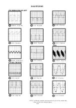
Page 12: ... schematic diagram H 1 WAVEFORMS 1V 0 5ms div 9 4 200mV 20µs div 13 0 5V 20µs div 8 1V 20µs div 2 2V 500µs div 12 1V 20µs div 1V 20µs div 11 0 5V 20µs div 6 2V 500µs div 1 10 20V 20µs div 5 200mV 5ms div 7 0 5V 20µs div 14 MICON TUNER IF CHROMA SOUND AMP 3 1V 0 1µs div 2V 200 µs div 15 2V 200µs div ...

Page 13: ...iagram H 2 22 200V 20µs div 23 10V 5ms div 24 20V 5ms div 25 50KV 20µs div 21 10V 20µs div WAVEFORMS JACK 28 200mV 20µs div 30 0 2V 0 2ms div 29 0 2V 0 2ms div 27 50KV 20µs div 26 50KV 20µs div 16 200mV 20µs div 17 0 5V 5ms div 50mV 0 5ms div 18 IF CHROMA SOUND AMP 20 50V 20µs div DEFLECTION CRT 19 20V 5ms div ...

Page 14: ...T TEXT 0 5V 20ns div 31 WAVEFORMS NOTE The following waveforms were measured at the point of the corresponding balloon number in the schematic diagram H 3 ...

Page 15: ...P SW106 EVQPB105K 20 CH UP 14 DOWN SW107 EVQPB105K 20 CH DOWN THE DC VOLTAGE AT EACH PART WAS MEASURED WITH THE DIGITAL TESTER WHEN THE COLOR BROADCAST WAS RECEIVED IN GOOD CONDITION AND PICTURE IS NORMAL NOTE OF PRINTING AND SUBJECT TO CHANGE WITHOUT NOTICE NOTE THIS SCHEMATIC DIAGRAM IS THE LATEST AT THE TIME BT001 R03 AB E_20_T BT002 R03 AB E_20_T TM101 R25 1190 Q103 DTC114TKA BUFFER CAUTION DI...

Page 16: ... KS C644 1000 6 3V YK C618 1 50V KS C303 1 50V KS C208 470 6 3V YK L301 15uH L604 10uH 0607 L202 1uH L603 10uH TP202 C212 0 47 50V KS C412 3 3 50V YK C626 0 47 50V KS C620 470 6 3V YK C213 0 47 50V KS C308 10 50V YK C313 1 50V KS C632 10 50V KS C628 470 6 3V YK C609_1 0 1 50V KS C647_1 10 50V KS W893 W812 W813 W802 W849 W871 W873 W900 W902 W855 W865 W803 W864 W915 THE DC VOLTAGE AT EACH PART WAS M...

Page 17: ...9 W877 THE DC VOLTAGE AT EACH PART WAS MEASURED WITH THE DIGITAL TESTER WHEN THE COLOR BROADCAST WAS RECEIVED IN GOOD CONDITION AND PICTURE IS NORMAL NOTE THE DC VOLTAGE AT EACH PART WAS MEASURED WITH THE DIGITAL TESTER WHEN THE COLOR BROADCAST WAS RECEIVED IN GOOD CONDITION AND PICTURE IS NORMAL NOTE SOUND_SP SOUND_SP AV HEAD PHONE SCHEMATIC DIAGRAM FROM CHOMA SOUND AMP G 6 G 5 PCB010 TM9440 1 2 ...

Page 18: ... C504 100P 500V CH C501_1 0 22 250V ECQUL C522 0 01 B C508 0 0022 500V B C529 470P 500V B C511 820P B C510 0 0018 M D513 1SS133 C519 100 160V C520 100 25V YK C517 470 25V YK C503 100 25V YK C521 1 50V KS C505 100 400V USP TP501 C518 1 50V KS C524 47 160V BXA D514 MTZJ3 6B D516 MTZJ5 1B W863 W916 THE DC VOLTAGE AT EACH PART WAS MEASURED WITH THE DIGITAL TESTER WHEN THE COLOR BROADCAST WAS RECEIVED ...

Page 19: ... 820P 2KV BP C429 0 0022 B C437 0 39 250V ECWF C804 470P B C807 470P B C810 560P B C820 0 001 B C806 0 0022 2KV B C802_1 100P B C440 470P 500V B C435 0 1 100V TF C416_1 0 012 100V PP C415_1 100P 500V B C427 10 50V MHE C425 4 7 50V KS C410 470 35V YK C417 3 3 50V KS L410 4 7mH 0909 L406 18uH TP802 RED TP803 GREEN TP801 BULE C413 1 250V YK C426 470 6 3V YK C414 100 35V YK C446 1 160V YK C418 1000 25...

Page 20: ...0 22uH L756 22uH C751 10 50V YK C774 10 50V KS C753 10 50V KS C777 10 50V YK C767 470 10V YK C775_1 22 50V YK W841 W848 W851 W835 W885 W891 W853 W854 W852 W859 THE DC VOLTAGE AT EACH PART WAS MEASURED WITH THE DIGITAL TESTER WHEN THE COLOR BROADCAST WAS RECEIVED IN GOOD CONDITION AND PICTURE IS NORMAL NOTE OF PRINTING AND SUBJECT TO CHANGE WITHOUT NOTICE NOTE THIS SCHEMATIC DIAGRAM IS THE LATEST A...

Page 21: ...24 W889 W822 THE DC VOLTAGE AT EACH PART WAS MEASURED WITH THE DIGITAL TESTER WHEN THE COLOR BROADCAST WAS RECEIVED IN GOOD CONDITION AND PICTURE IS NORMAL NOTE OF PRINTING AND SUBJECT TO CHANGE WITHOUT NOTICE NOTE THIS SCHEMATIC DIAGRAM IS THE LATEST AT THE TIME AV1 YS_MUTE FBT_5V DET_OUT AV_VIDEO_1 VIDEO_OUT AV_VIDEO 21 R A R 21 G A G 21 B A B A Y 21 Y GND GND FROM JACK FROM TO CHROMA SOUND AMP ...

Page 22: ...B105K 20 CH UP 14 DOWN SW107 EVQPB105K 20 CH DOWN THE DC VOLTAGE AT EACH PART WAS MEASURED WITH THE DIGITAL TESTER WHEN THE COLOR BROADCAST WAS RECEIVED IN GOOD CONDITION AND PICTURE IS NORMAL NOTE OF PRINTING AND SUBJECT TO CHANGE WITHOUT NOTICE NOTE THIS SCHEMATIC DIAGRAM IS THE LATEST AT THE TIME BT001 R03 AB E_20_T BT002 R03 AB E_20_T TM101 SBER00187A S802Y Q103 DTC114TKA BUFFER CAUTION DIGITA...

Page 23: ...02 1uH L603 10uH L605 27uH TP202 C620 470 6 3V YK C609_1 0 1 50V KS C626 0 47 50V KS C308 10 50V YK C212 0 47 50V KS C213 0 47 50V KS C313 1 50V KS C632 10 50V KS C628 470 6 3V YK C622_1 1 50V YK C647_1 10 50V KS C412 3 3 50V YK W803 W893 W812 W813 W802 W849 W871 W873 W900 W902 W855 W904 W865 W864 THE DC VOLTAGE AT EACH PART WAS MEASURED WITH THE DIGITAL TESTER WHEN THE COLOR BROADCAST WAS RECEIVE...

Page 24: ... W877 THE DC VOLTAGE AT EACH PART WAS MEASURED WITH THE DIGITAL TESTER WHEN THE COLOR BROADCAST WAS RECEIVED IN GOOD CONDITION AND PICTURE IS NORMAL NOTE THE DC VOLTAGE AT EACH PART WAS MEASURED WITH THE DIGITAL TESTER WHEN THE COLOR BROADCAST WAS RECEIVED IN GOOD CONDITION AND PICTURE IS NORMAL NOTE SOUND_SP SOUND_SP AV HEAD PHONE SCHEMATIC DIAGRAM FROM CHROMA SOUND AMP G 6 G 5 PCB010 TM9440 1 2 ...

Page 25: ...512 0 015 M C504 100P 500V CH C522 0 01 B C508 0 0022 500V B C529 470P 500V B C511 820P B C510 0 0018 M D513 1SS133 C520 100 25V YK C517 470 25V YK C503 100 25V YK C521 1 50V KS C505 100 400V USP C519 100 160V TP501 C518 1 50V KS C524 47 160V BXA D514 MTZJ3 6B D516 MTZJ5 1B W863 W916 THE DC VOLTAGE AT EACH PART WAS MEASURED WITH THE DIGITAL TESTER WHEN THE COLOR BROADCAST WAS RECEIVED IN GOOD COND...

Page 26: ...37 0 39 250V ECWF C804 470P B C807 470P B C810 560P B C820 0 001 B C806 0 0022 2KV B C802_1 100P B C423 0 015 M C440 470P 500V B C435 0 1 100V TF C416_1 0 012 100V PP C415_1 100P 500V B C427 10 50V MHE C425 4 7 50V KS C410 470 35V YK C417 3 3 50V KS L410 4 7mH 0909 L406 18uH TP802 RED TP803 GREEN TP801 BULE C413 1 250V YK C426 470 6 3V YK C414 100 35V YK C446 1 160V YK C418_1 2200 25V MHE C433 470...

Page 27: ...1 10 50V YK C774 10 50V KS C753 10 50V KS C777 10 50V YK C767 470 10V YK C775_1 22 50V YK W851 W859 W841 W848 W835 W885 W891 W853 W854 W852 THE DC VOLTAGE AT EACH PART WAS MEASURED WITH THE DIGITAL TESTER WHEN THE COLOR BROADCAST WAS RECEIVED IN GOOD CONDITION AND PICTURE IS NORMAL NOTE OF PRINTING AND SUBJECT TO CHANGE WITHOUT NOTICE NOTE THIS SCHEMATIC DIAGRAM IS THE LATEST AT THE TIME FOR_VCR F...

Page 28: ...YK C640 10 50V YK C638 1 50V YK C637_1 10 50V KS C648_1 1 50V KS W879 W889 THE DC VOLTAGE AT EACH PART WAS MEASURED WITH THE DIGITAL TESTER WHEN THE COLOR BROADCAST WAS RECEIVED IN GOOD CONDITION AND PICTURE IS NORMAL NOTE OF PRINTING AND SUBJECT TO CHANGE WITHOUT NOTICE NOTE THIS SCHEMATIC DIAGRAM IS THE LATEST AT THE TIME AV1 YS_MUTE TEXT R TEXT G TEXT B TEXT Y GND FBT_5V DET_OUT AV_VIDEO_1 AV_V...

Page 29: ...022 B C867 0 01 B C854 220P CH C852 1 TF C851 0 001 B C856 27P CH C865 100 6 3V YK C868 100 6 3V YK L850 1 5uH L852 10uH L851 10uH W860 W855 W851 THE DC VOLTAGE AT EACH PART WAS MEASURED WITH THE DIGITAL TESTER WHEN THE COLOR BROADCAST WAS RECEIVED IN GOOD CONDITION AND PICTURE IS NORMAL NOTE OF PRINTING AND SUBJECT TO CHANGE WITHOUT NOTICE NOTE THIS SCHEMATIC DIAGRAM IS THE LATEST AT THE TIME T T...

Reviews: