background image

MS-9988

COM Express Carrier Board

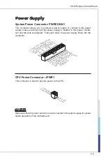
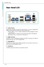
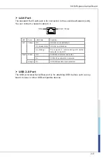
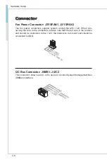
Summary of Contents for MS-9988

Page 1: ... MS 9988 COM Express Carrier Board ...

Page 2: ...ation Intel is a registered trademark of Intel Corporation Windows is a registered trademark of Microsoft Corporation AMI is a registered trademark of Advanced Micro Devices Inc Award is a registered trademark of Phoenix Technologies Ltd Realtek is a registered trademark of Realtek Semiconductor Corporation Revision History Revision Date V1 0 2014 06 Technical Support If a problem arises with your...

Page 3: ...y add on card or mod ule All cautions and warnings on the equipment should be noted Never pour any liquid into the opening that could damage or cause electrical shock If any of the following situations arises get the equipment checked by ser vice personnel The power cord or plug is damaged Liquid has penetrated into the equipment The equipment has been exposed to moisture The equipment does not wo...

Page 4: ...s unsorted household waste Please use the public collection system to return recycle or treat them in compliance with the local regulations Taiwan For better environmental protection waste batteries should be collected separately for recycling or special disposal California USA The button cell battery may contain perchlorate material and requires special handling when recycled or disposed of in Ca...

Page 5: ...e 1 The changes or modifications not expressly approved by the party responsible for compliance could void the user s authority to operate the equipment Notice 2 Shielded interface cables and AC power cord if any must be used in order to comply with the emission limits VOIR LA NOTICE D INSTALLATION AVANT DE RACCORDER AU RESEAU This device complies with Part 15 of the FCC Rules Operation is subject...

Page 6: ...adio Frequency Interference Statement v WEEE Statement v 1 Overview 1 1 Specifications 1 2 Board Layout 1 4 2 Hardware Setup 2 1 Power Supply 2 3 Rear Panel I O 2 4 Connector 2 6 Jumper 2 18 Slot 2 20 3 BIOS Setup 3 1 Entering Setup 3 2 The Menu Bar 3 4 Main 3 5 Advanced 3 6 Boot 3 13 Security 3 14 Chipset 3 19 Power 3 21 Save Exit 3 23 Appendix WDT GPIO A 1 WDT Sample Code A 2 GPIO Sample Code A ...

Page 7: ...s Carrier Board It is a highly advanced feature rich car rier that offers PCIe and Mini PCIe expansion This carrier board also features USB 3 0 USB 2 0 ports a VGA port DisplayPorts LVDS inter face a parallel port connector serial port connectors audio jacks SATA ports etc 1 Overview ...

Page 8: ...in Headers Connectors Jumpers 1 24 pin power connector 1 4 pin power connector 2 system fan connectors 2 SATA 6Gb s ports 2 SATA 3Gb s ports 1 front panel connector 1 front audio connector 1 parallel port connector 2 RS 232 serial port connectors 2 GPIO pin headers 2 SMBus connectors 1 USB 2 0 connector 1 port 1 LVDS connector 1 keyboard mouse connector 1 inverter power connector 2 BIOS select jum...

Page 9: ...d Expansion Slots 1 PCIe x16 slot 6 PCIe x1 slots 1 Mini PCIe slot Form Factor ATX form factor 12 x 9 6 Compliance PICMG COM Express R2 0 Type 6 Environmental Operating Temperature 0o C 60o C Storage Temperature 20o C 80o C Humidity 5 90 RH Non Condensing ...

Page 10: ...Keyboard Mouse Connector COM Port Power Jumper Power Connector SMBus Connector Front Panel Connector PCIe Slot COM Express Connector Inverter Power Connector Inverter Power Jumper LVDS Power Jumper SMBus Connector BIOS Select Jumper LVDS Connector GPIO Pin Header System Fan Connector PCIe Slot Power Connector USB 3 0 Port Line In Mic In USB 2 0 Port DisplayPort Line Out USB 3 0 Port LAN Port VGA P...

Page 11: ...llation be careful in holding the com ponents and follow the installation procedures For some components if you install in the wrong orientation the components will not work prop erly Use a grounded wrist strap before handling computer components Static electricity may damage the components 2 Hardware Setup ...

Page 12: ...2 0 Connector JUSB1 2 9 Serial Port Connector JCOM1 JCOM2 2 9 LVDS Inverter Connector JINVDD1 2 10 LVDS Connector JLVDS1 2 10 Front Audio Connector JAUD1 2 11 Parallel Port Connector JLPT1 2 11 TPM Module Connector JDP1 2 12 COM Express Connectors 2 13 Jumper 2 18 Clear CMOS Jumper JCMOS1 2 18 AT ATX Select Jumper JAT_ATX1 2 18 COM Port Power Jumper VCOM1 VCOM2 2 19 BIOS Select Jumper JBIOS1 JBIOS...

Page 13: ...to the connector 1 3 3 3 V 1 3 3 V 1 4 1 2 V 2 3 3 V 1 5 G r o u n d 3 G r o u n d 1 6 P S O N 4 5 V 1 7 G r o u n d 5 G r o u n d 1 8 G r o u n d 6 5 V 1 9 G r o u n d 7 G r o u n d 2 2 5 V 1 0 1 2 V 2 0 5 V 8 P W R O K 2 3 5 V 1 1 1 2 V 2 1 5 V 9 5 V S B 2 4 G r o u n d 1 2 3 3 V CPU Power Connector JPWR1 This connector is used to provide power to the CPU 4 1 2 V 2 G r o u n d 3 1 2 V 1 G r o u ...

Page 14: ...lue Line In is used for external CD player tapeplayer or other audio devices Line Out Green Line Out is a connector for speakers or headphones Mic Pink Mic is a connector for microphones USB 3 0 Port The USB 3 0 port is backward compatible with USB 2 0 devices and supports data transfer rate up to 5 Gbit s SuperSpeed DisplayPort DisplayPort is a digital display interface standard This connector is...

Page 15: ...on Left Yellow Off LAN link is not established On steady state LAN link is established On blinking The computer is communicating with another computer on the LAN Right Green Off 10 Mbit sec data rate is selected On 100 Mbit sec data rate is selected Orange On 1000 Mbit sec data rate is selected USB 2 0 Port The USB Universal Serial Bus port is for attaching USB devices such as key board mouse or o...

Page 16: ... cooling fan with 12V When con necting the wire to the connectors always note that the red wire is the positive and should be connected to the 12V the black wire is Ground and should be connected to GND I2C Bus Connector JSMB1 JI2C2 This connector known as I2C is for users to connect System Management Bus SMBus interface ...

Page 17: ...r the General Purpose Input Output GPIO periph eral module Serial ATA Connector SATA1 SATA4 This connector is a high speed Serial ATA interface port Each connector can connect to one Serial ATA device Important Please do not fold the SATA cable into a 90 degree angle Otherwise data loss may occur during transmission ...

Page 18: ...KBMS1 This connector is provided to connect a keyboard and a mouse Front Panel Connector JFP1 This front panel connector is provided for electrical connection to the front panel switches LEDs and is compliant with Intel Front Panel I O Connectivity Design Guide ...

Page 19: ...e that the pins of VCC and GND must be connected correctly to avoid possible damage Serial Port Connector JCOM1 JCOM2 This connector is a 16550A high speed communications port that sends receives 16 bytes FIFOs You can attach a serial device to it PIN SIGNAL DESCRIPTION 1 2 3 4 5 6 7 8 9 DCD RXD TXD DTR GND DSR RTS CTS VCC_COM Data Carrier Detect Receive Data Transmit Data Data Terminal Ready Sign...

Page 20: ... A _ D A T A 1 1 1 L V D S _ B L O N 9 L _ B K L T _ C T R L 7 L V D S _ D D C _ C L K 5 L C D _ V D D 3 L C D _ V D D 1 1 2 V 4 0 L V D S A _ C L K 2 8 L V D S B _ D A T A 0 2 6 L V D S B _ D A T A 0 2 4 G N D 2 2 L V D S A _ D A T A 2 2 0 L V D S A _ D A T A 2 1 8 G N D 1 6 L V D S A _ D A T A 0 1 4 L V D S A _ D A T A 0 1 2 L V D S _ D E T E C T _ C 1 0 L V D S _ V D D _ E N 8 L V D S _ D D C _...

Page 21: ...tional parallel port bracket The parallel port is a standard printer port that supports Enhanced Parallel Port EPP and Extended Capabilities Parallel Port ECP mode 1 R S T B 3 P R N D 0 5 P R N D 1 7 P R N D 2 9 P R N D 3 1 1 P R N D 4 1 3 P R N D 5 1 5 P R N D 6 1 7 P R N D 7 1 9 A C K 2 1 B U S Y 2 3 P E 2 5 S L C T 1 0 G r o u n d 1 4 G r o u n d 8 L P T _ S L I N 1 2 G r o u n d 6 P I N I T 4 ...

Page 22: ...atform manual for more details 1 0 N o P i n 1 4 G r o u n d 8 5 V P o w e r 1 2 G r o u n d 6 S e r i a l I R Q 4 3 3 V P o w e r 2 3 V S t a n d b y p o w e r 1 L P C C l o c k 3 L P C R e s e t 5 L P C a d d r e s s d a t a p i n 0 7 L P C a d d r e s s d a t a p i n 1 9 L P C a d d r e s s d a t a p i n 2 1 1 L P C a d d r e s s d a t a p i n 3 1 3 L P C F r a m e ...

Page 23: ...ss Connectors The COM Express connectors are used to interface the COM Express carrier board to a module board Connect the COM Express connectors on the carrier board as indicated below to the COM Express connectors on the module board D1 C1 B1 A1 D110 C110 B110 A110 ...

Page 24: ...LK_AUX A16 SATA0_TX B16 SATA1_TX C16 DDI1_PAIR6 D16 DDI1_CTRL DATA_AUX A17 SATA0_TX B17 SATA1_TX C17 RSVD D17 RSVD A18 SUS_S4 B18 SUS_STAT C18 RSVD D18 RSVD A19 SATA0_RX B19 SATA1_RX C19 PCIE_RX6 D19 PCIE_TX6 A20 SATA0_RX B20 SATA1_RX C20 PCIE_RX6 D20 PCIE_TX6 A21 GND FIXED B21 GND FIXED C21 GND FIXED D21 GND FIXED A22 SATA2_TX B22 SATA3_TX C22 PCIE_RX7 D22 PCIE_TX7 A23 SATA2_TX B23 SATA3_TX C23 P...

Page 25: ...C48 RSVD D48 RSVD A49 E X C D 0 _ CPPE B49 SYS_RESET C49 DDI3_PAIR1 D49 DDI2_PAIR3 A50 LPC_SERIRQ B50 CB_RESET C50 DDI3_PAIR3 D50 DDI2_PAIR3 A51 GND FIXED B51 GND FIXED C51 GND FIXED D51 GND FIXED A52 PCIE_TX5 B52 PCIE_RX5 C52 PEG_RX0 D52 PEG_TX0 A53 PCIE_TX5 B53 PCIE_RX5 C53 PEG_RX0 D53 PEG_TX0 A54 GPI0 B54 GPO1 C54 TYPE0 D54 P E G _ L A N _ RV A55 PCIE_TX4 B55 PCIE_RX4 C55 PEG_RX1 D55 PEG_TX1 A5...

Page 26: ... 2 C _ DAT B84 VCC_5V_SBY C84 GND D84 GND A85 GPI3 B85 VCC_5V_SBY C85 PEG_RX10 D85 PEG_TX10 A86 KBD_RST B86 VCC_5V_SBY C86 PEG_RX10 D86 PEG_TX10 A87 K B D _ A20GATE B87 VCC_5V_SBY C87 GND D87 GND A88 P C I E 0 _ C K _ REF B88 BISO_DIS1 C88 PEG_RX11 D88 PEG_TX11 A89 P C I E 0 _ C K _ REF B89 VGA_RED C89 PEG_RX11 D89 PEG_TX11 A90 GND FIXED B90 GND FIXED C90 GND FIXED D90 GND FIXED A91 SPI _POWER B91...

Page 27: ... VCC_12V B105 VCC_12V C105 VCC_12V D105 VCC_12V A106 VCC_12V B106 VCC_12V C106 VCC_12V D106 VCC_12V A107 VCC_12V B107 VCC_12V C107 VCC_12V D107 VCC_12V A108 VCC_12V B108 VCC_12V C108 VCC_12V D108 VCC_12V A109 VCC_12V B109 VCC_12V C109 VCC_12V D109 VCC_12V A110 GND FIXED B110 GND FIXED C110 GND FIXED D110 GND FIXED ...

Page 28: ...ation With the CMOS RAM the system can automatically boot OS every time it is turned on If you want to clear the system configuration set the jumper to clear data 1 1 Normal Clear CMOS Important You can clear CMOS by shorting 2 3 pin while the system is off Then return to 1 2 pin position Avoid clearing the CMOS while the system is on it will damage the motherboard AT ATX Select Jumper JAT_ATX1 Th...

Page 29: ...IOS code short connect pin 2 3 first Under normal operation we suggest that you enable the BIOS flash protection by short connecting pin 1 2 to protect the system BIOS from virus infection JBIOS1 JBIOS2 Description 1 1 Enable Carrier Board Flash ROM Default 1 1 Enable Module Board Flash ROM LVDS Power Jumper JVDD1 Use this jumper to specify the operation voltage of the LVDS interface flat panel 3V...

Page 30: ...press Slot The Mini PCIe slot is provided for wireless LAN cards TV tuner cards Robson NAND Flash cards and other Mini PCIe cards Important When adding or removing expansion cards make sure that you unplug the power supply first Meanwhile read the documentation for the expansion card to config ure any necessary hardware or software settings for the expansion card such as jumpers switches or BIOS c...

Page 31: ...message appears on the screen at system startup and re quests users to run SETUP Users want to change the default settings for customized features Important Please note that BIOS update assumes technician level experience As the system BIOS is under continuous update for better system performance the illustrations in this chapter should be held for reference only 3 BIOS Setup ...

Page 32: ...you respond and you still wish to enter Setup restart the system by turning it OFF and On or pressing the RESET button You may also restart the system by simultaneously pressing Ctrl Alt and De lete keys Important The items under each BIOS category described in this chapter are under continuous update for better system performance Therefore the description may be slightly different from the latest...

Page 33: ...ou find a right pointer symbol appears to the left of certain fields that means a sub menu can be launched from this field A sub menu contains additional op tions for a field parameter You can use arrow keys to highlight the field and press Enter to call up the sub menu Then you can use the control keys to enter values and move from field to field within a sub menu If you want to return to the mai...

Page 34: ...specify the priority of boot devices Security Use this menu to set supervisor and user passwords Chipset This menu controls the advanced features of the onboard chipsets Power Use this menu to specify your settings for power management Save Exit This menu allows you to load the BIOS default values or factory default settings into the BIOS and exit the BIOS setup utility with or without changes ...

Page 35: ...his setting allows you to set the system date The date format is Day Month Date Year System Time This setting allows you to set the system time The time format is Hour Minute Second SATA Mode Selection This setting specifies the SATA controller mode ...

Page 36: ... the booting sequence This delay ensures that the logo is displayed for a suf ficient amount of time Therefore it is recommended that you disable this BIOS feature for a faster boot up time Bootup NumLock State This setting is to set the Num Lock status when the system is powered on Setting to On will turn on the Num Lock key when the system is powered on Setting to Off will allow users to use the...

Page 37: ...is setting disables enables the USB XHCI controller The eXtensible Host Controller Interface XHCI is a computer interface specification that defines a register level description of a Host Controller for Universal Serial bus USB which is capable of interfacing to USB 1 0 2 0 and 3 0 compatible devices The specification is also referred to as the USB 3 0 Host Controller specifica tion Legacy USB Sup...

Page 38: ... cious buffer overflow attacks when combined with a supporting operating system This functionality allows the processor to classify areas in memory by where application code can execute and where it cannot When a malicious worm attempts to insert code in the buffer the processor disables code execu tion preventing damage or worm propagation Intel Virtualization Technology Virtualization enhanced b...

Page 39: ...timer a hardware timer that generates a reset when the software that it monitors does not respond as expected each time the watch dog polls it IT8518 H W Monitor the Compact Module These items display the current status of all monitored hardware devices components such as voltages temperatures and all fans speeds ...

Page 40: ... Fan function Smart Fan is an excel lent feature which will adjust the CPU system fan speed automatically de pending on the current CPU system temperature avoiding the overheating to damage your system Super IO Configuration the Carrier Board Serial Port 1 Serial Port 2 This setting enables disables the specified serial port ...

Page 41: ...ort Device Mode Select an operation mode for the parallel port FIFO Mode This setting controls the FIFO data transfer mode Shared IRQ Mode This setting provides the system with the ability to share interrupts among its serial ports Watch Dog Timer You can enable the system watch dog timer a hardware timer that generates a reset when the software that it monitors does not respond as expected each t...

Page 42: ...s temperatures and all fans speeds Smart Fan Configuration the Carrier Board Smart SYSFAN1 SYSFAN2 Target These settings enable disable the Smart Fan function Smart Fan is an excel lent feature which will adjust the CPU system fan speed automatically de pending on the current CPU system temperature avoiding the overheating to damage your system ...

Page 43: ...ere BIOS at tempts to load the disk operating system Hard Drive BBS Priorities This setting allows users to set the priority of the specified devices First press Enter to enter the sub menu Then you may use the arrow keys to select the desired device then press or PageUp PageDown key to move it up down in the priority list ...

Page 44: ...tup Security Administrator Password Administrator Password controls access to the BIOS Setup utility User Password User Password controls access to the system at boot and to the BIOS Setup utility Trusted Computing ...

Page 45: ...en set to Disable the OS will not show security device TCG EFI protocol and INT1A interface will not be available Intel TXT LT Configuration Intel TXT LT Support Intel TXT Trusted Execution Technology can only be enabled disabled if SMX is enabled VT and VT d support must also be enabled prior to TXT PCH FW Configuration ...

Page 46: ...es disables the MDES BIOS status code Firmware Update Configuration ME FW Image Re Flash This setting enables disables the ME FW image reflash Intel R Anti Theft Technology Configuration Intel Anti Theft Technology is hardware based technology that can lock a lost or stolen system so that personal confidential information is protected and inacces sible by unauthorized users ...

Page 47: ...ion Console Redirection operates in host systems that do not have a monitor and keyboard attached This setting enables disables the operation of console re direction When set to Enabled BIOS redirects and sends all contents that should be displayed on the screen to the serial COM port for display on the terminal screen Besides all data received from the serial port is interpreted as keystrokes fro...

Page 48: ... from one device to another to ensure that the receiving device can handle all of the incoming data This is particularly important where the sending device is capable of sending data much faster than the receiving device can receive it VT UTF8 Combo Key Support This setting enables disables the VT UTF8 combination key support for ANSI VT100 terminals Recorder Mode Resolution 100x31 These settings ...

Page 49: ...llocated This setting defines the DVMT pre allocated memory Pre allocated memory is the small amount of system memory made available at boot time by the system BIOS for video Pre allocated memory is also known as locked memory This is because it is locked for video use only and as such is invisible and unable to be used by the operating system DVMT Total Gfx Mem This setting specifies the memory s...

Page 50: ...3 20 BIOS Setup LCD Panel Type This setting allows you to set the resolution of the LCD display Panel Color Depth This item is used for setting the matching panel color depth ...

Page 51: ... Leaves the computer in the power on state Last State Restores the system to the previous status before power failure or interrupt occurred Deep S5 The setting enables disables the Deep S5 power saving mode S5 is almost the same as G3 Mechanical Off except that the PSU still supplies power at a mini mum to the power button to allow return to S0 A full reboot is required No previ ous content is ret...

Page 52: ...fies whether the system will be awakened from power saving modes when activity or input signal of onboard PCIE PCI PME is detected Ring An input signal on the serial Ring Indicator RI line in other words an incoming call on the modem awakens the system from a soft off state RTC When Enabled your can set the date and time at which the RTC real time clock alarm awakens the system from suspend mode ...

Page 53: ...anges and exit the Setup Utility Discard Changes Abandon all changes Load Optimized Defaults Use this menu to load the default values set by the motherboard manufacturer specifically for optimal performance of the motherboard Save as User Defaults Save changes as the user s default profile Restore User Defaults Restore the user s default profile ...

Page 54: ......

Page 55: ...2 A 1 This appendix provides the sample codes of WDT Watch Dog Timer and GPIO General Purpose Input Output Appendix WDT GPIO ...

Page 56: ...l Change to WDT mov dx SIO_INDEX_Port mov al 07h out dx al mov dx SIO_DATA_Port mov al WatchDog_LDN out dx al Acive WDT mov dx SIO_INDEX_Port mov al 30h out dx al mov dx SIO_DATA_Port in al dx or al 01h out dx al set timer mov dx SIO_INDEX_Port mov al 0F6h out dx al mov dx SIO_DATA_Port mov al WDT_Timer out dx al set UINT mov dx SIO_INDEX_Port mov al 0F5h out dx al mov dx SIO_DATA_Port mov al WDT_...

Page 57: ...equ 04Eh SIO_DATA_Port equ 04Fh SIO_UnLock_Value equ 087h SIO_Lock_Value equ 0AAh SIO_LDN_GPIO equ 06h GPI_REG equ 0B2h GPO_REG equ 0B1h GPO0_Value equ 00010000b Sample Code 1 Get GPI 0 status Enable config mode mov dx SIO_INDEX_Port mov al SIO_UnLock_Value out dx al jmp short 2 Io_delay jmp short 2 Io_delay out dx al Switch GPIO Configuration for SIO LDN 0x06 mov dx SIO_INDEX_Port mov al 07h out ...

Page 58: ...SIO_UnLock_Value out dx al jmp short 2 Io_delay jmp short 2 Io_delay out dx al Switch GPIO Configuration for SIO LDN 0x06 mov dx SIO_INDEX_Port mov al 07h out dx al mov dx SIO_DATA_Port mov al SIO_LDN_GPIO out dx al Set GPO 0 Register mov dx SIO_INDEX_Port mov al GPO_REG out dx al mov dx SIO_DATA_Port in al dx and al not GPO0_Value clear al bit4 GPO 0 or al GPO0_Value set GPO 0 out dx al Exit SIO ...

Page 59: ...r 16h Bit 0 1 2 3 Sample code 2 INDEX_Port equ 066h DATA_Port equ 062h Read_cmd equ 080h Write_cmd equ 081h GPI_REG equ 016h GPO_REG equ 016h GPO0_Value equ 00000001b Sample Code 1 Get GPI 0 status Enable config mode mov dx INDEX_Port mov al Read_cmd out dx al jmp short 2 Io_delay jmp short 2 Io_delay Get GPI 0 Pin Status Register mov dx DATA_Port mov al GPI_REG out dx al mov dx DATA_Port in al dx...

Page 60: ...rt 2 Io_delay mov dx DATA_Port mov al GPI_REG out dx al mov dx DATA_Port in al dx and al not GPO0_Value clear al bit GPO 0 or al GPO0_Value set GPO 0 mov bl al mov dx INDEX_Port mov al Write_cmd out dx al jmp short 2 Io_delay jmp short 2 Io_delay mov dx DATA_Port mov al GPO_REG out dx al mov dx DATA_Port mov al bl out dx al ...

Reviews: