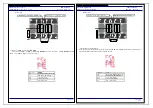
NAITO DENSEI MACHIDA MFG.CO.,LTD.
RL78/H1D ターゲット・ボード
FB-R5F11PLG-TB ユーザーズ・マニュアル
ユーザーズ・マニュアル
SBAL-190028-00
Rev 1.00 2019.1.15
本製品は、ルネサス エレクトロニクス製のプログラミング機能付きオンチップ・デバッグ・エミュレータ E1 を使用して、マイコンの動作を試
すためのターゲット・ボードです。
①RL78/H1D ターゲット・ボード(FB-R5F11PLG-TB)の特徴
●RL78/H1D(R5F11PLG)搭載
●8MHz と 32.768KHz の発振子を搭載
●ユニバーサル・エリア(2.54mm ピッチ)を搭載
●フラッシュ・メモリ・プログラミング、オンチップ・デバッグに両対応(TOOL0 端子使用)
●マイコンの端子を周辺ボード・コネクタに配置した高拡張性
●基板を切り離すことで小型にすることが可能
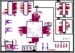
②ハードウエア仕様
CPU R5F11PLG
メイン・システム・クロック動作周波数
8MHz(ボード上の発振子を使う場合)
サブシステム・クロック動作周波数
32.768KHz(ボード上に搭載)
搭載部品
CN3:E1 接続用コネクタ(14pin)
CN4,CN5: アプリケーションボードコネクタ *1
Power LED: 赤 x1(LED2)
評価用 LED: 黄 x1(LED1 は P77 へ接続)
評価用 SW: SW1(INTP0 へ接続)
メイン・システム・クロック(OSC1): 8MHz 発振子(X1,X2 へ接続)
サブシステム・クロック(OSC2): 32.768KHz 発振子(XT1,XT2 へ接続)
未実装部品
周辺ボードコネクタ(2.54mm ピッチ) 50pinx2:CN1,CN2, プルアップ抵抗(R8,R9)
3.0V レギュレータ回路:レギュレータ(IC2),コンデンサ(C10,C11),抵抗(R7),フィルタ(L1)
動作電圧
2.4V~5.5V(OSC1:8MHz 発振子使用時)
*1.アプリケーションボードはセンサを搭載し、ヘルスケアなどの具体的なアプリケーションをお試しいただけるボードです。(別売)
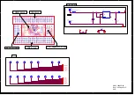
③寸法、部品配置など
<Top View>
基板上のパターン
について:パターンをカットすることで、その回路はオープンとなります。
再度接続させたい場合は半田ショートしてください。
回路図のパッドの表示 オープン:
ショート:
基板を切り離す際は,カッター等で切り込みを入れてから割ってください。
切り取り部分で基板両面のパターンがショートしないように配線が確実に切れていることを確認してください。
Page 1 of 5
10
20
30
40
1
2
CN2
50
49
CN1
30
40
20
10
50
49
1
2
VSS
VDD
AVSS
AVDD
SW1
TOOL0
P137
VDD
LED1
LED2
P77
P123 P124
XT2
X1 X2
P122
P121
RESET
CN3_EVDD
CN3_VDD
POWER
GND
AVSS AVDD
IC2
RL78/
H1D
Power LED
68.58mm
4
8
.2
6
m
m
CN1:周辺ボードコネクタ(未実装)
CN2:周辺ボードコネクタ(未実装)
評価用SW
評価用
LED
ユニバーサル・エリア
サブシステム・クロック
メイン・システム・クロック
ユニバーサル・エリア
E1接続用コネクタ
3.0V
レギュレータ
回路
ANALOG PAD
基板切り離し時のカット位置
NAITO DENSEI MACHIDA MFG.CO.,LTD.
RL78/H1D Target board
FB-R5F11PLG-
TB User’s Manual
User’s Manual
SBAL-190028-00
Rev 1.00 2019.1.15
The FB-R5F11PLG-TB is a target board used for evaluating microcontroller operations, using the E1, the Renesas Electronics
on-chip debug emulator with programming function (hereinafter referred to as E1).
(1) RL78/H1D
target board (FB-R5F11PLG-TB) features
● Incorporates RL78/H1D (R5F11PLG).
● A 8 MHz resonator and a 32.768 KHz resonator are mounted.
● Equipped with universal area (2.54 mm pitch)
● Supports both flash memory programming and on-chip debugging (using TOOL0 pin)
● Highly extendable; peripheral board connectors are equipped with microcontroller pins
● It can be made compact by cutting off this board.
(2) hardware specifications
CPU
R5F11PLG
Main system clock operating frequency
8MHz(when use resonator mounted on board)
Subsystem clock operating frequency
32.768KHz (mounted on board).
Embedded parts
CN3: For E1 connector (14-pin)
CN4,CN5: Aplication Board connector *
1
Power LED: Red
1 (LED2)
Test LED: Yellow
1 (LED1 connected to P77)
Test SW: SW1 (connected to INTP0)
Main system clock (OSC1): 8MHz resonator(connected to X1 and X2)
Subsystem clock (OSC2): 32.768 KHz resonator (connected to XT1 and XT2)
Unmouted parts
Peripheral board connectors (2.54 mm pitch) 50-pin
2:CN1,CN2, pulllup resister
(R8 and R9)
3.0V regulator Circuit:regulator(IC2),capacitor(C10,C11),resister(R7),filter(L1)
Operating voltage
2.4 to 5.5 V(when 8 MHz resonator used at OSC1)
*1.
An application board loads a sensor and is the board which can try application in detail of healthcare.
(
Sold separately
)
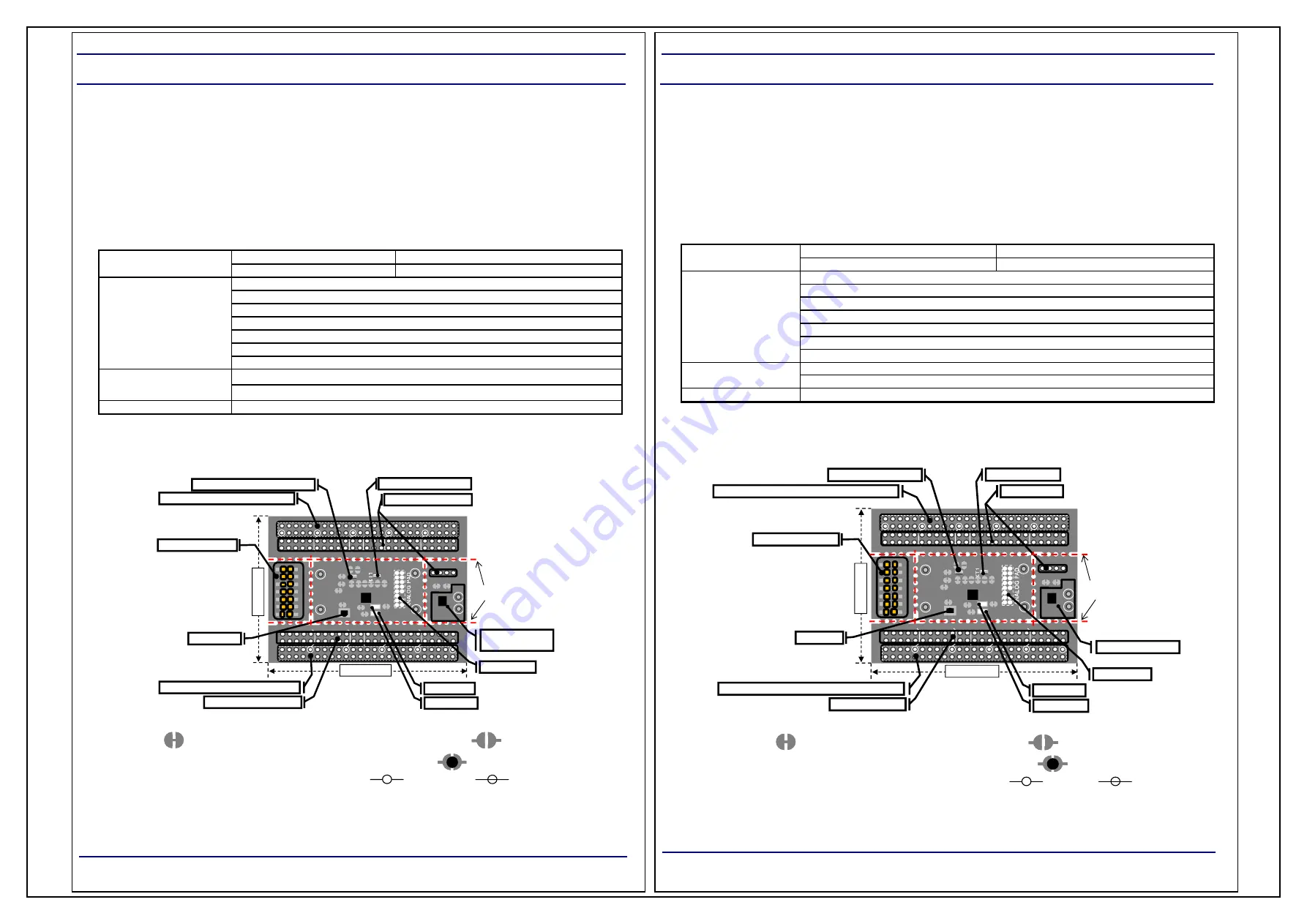
(3) Dimensions and parts layout
<Top view>
Pattern on the board
:
Splitting this wiring leaves open the relevant circuit (
).
To reconnect the circuit, short the circuit by soldering (
)..
Showing of the pad on circuit diagram. open:
short:
When cutting the board, please insert a notch with a cutter beforehand. Make sure that the wiring is reliably cut off so that the
pattern on both sides of the board does not short-circuit at the cut portion.
Page 1 of 5
A4D
10
20
30
40
1
2
CN2
50
49
CN1
30
40
20
10
50
49
1
2
VSS
VDD
AVSS
AVDD
SW1
TOOL0
P137
VDD
LED1
LED2
P77
P123 P124
XT2
X1 X2
P122
P121
RESET
CN3_EVDD
CN3_VDD
POWER
GND
AVSS AVDD
IC2
RL78/
H1D
Power LED
68.58mm
4
8
.2
6
mm
CN1:Peripheral Board connector(Unmount)
CN2:Peripheral Board connector(Unmount)
Test SW
Test LED
Universal area
Subsystem Clock
Main system Clock
Universal area
For E1 connection
3.0V regulator circuit
ANALOG PAD
Cutting point