USER GUIDE AND SPECIFICATIONS
NI 9144
Deterministic Ethernet Expansion Chassis for C Series Modules
This user guide describes how to connect the NI 9144 chassis to a network, how to use the
NI 9144 chassis features, and contains the NI 9144 chassis specifications. The NI 9144 is a slave
device and requires a compliant EtherCAT Master and network to function.
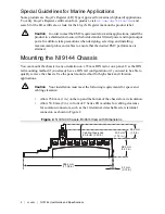
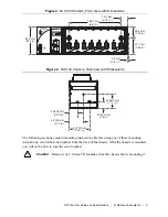
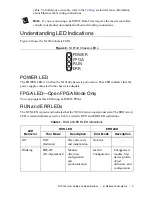
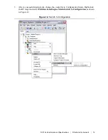
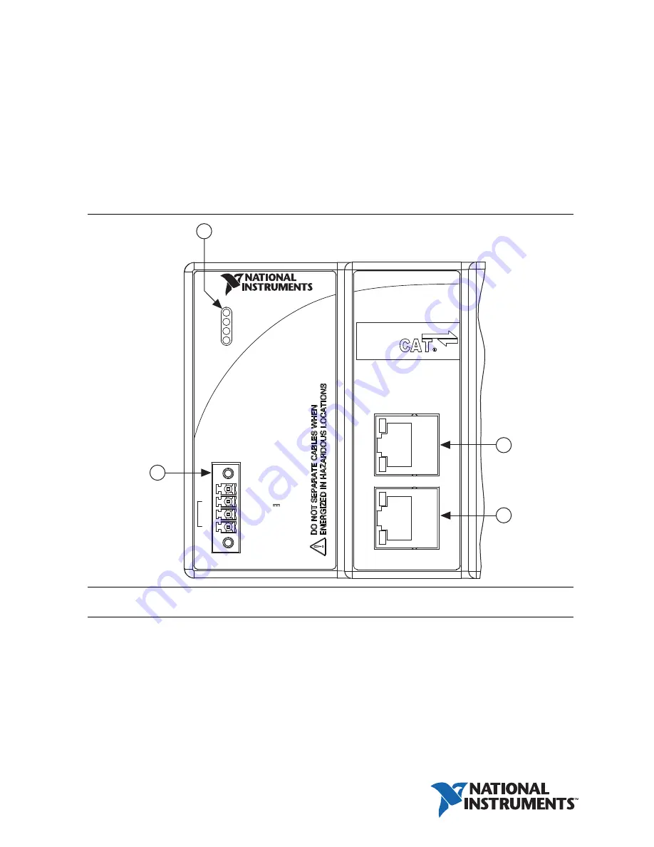
Figure 1.
NI 9144 Chassis
1
LEDs
2
IN Port
3
OUT Port
4
Power Connector
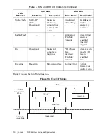
POWER
FPGA
RUN
ERR
Ether
NI 9144
INPUT
9-30 V
20 W MAX
V
C
C
NC
LINK/
ACT
OUT
IN
LINK/
ACT
4
1
2
3