
Transistors
1
Publication date: April 2003
SJC00226BED
2SD1819A
Silicon NPN epitaxial planar type
For general amplification
Complementary to 2SB1218A
■
Features
•
High forward current transfer ratio h
FE
•
Low collector-emitter saturation voltage V
CE(sat)
•
S-Mini type package, allowing downsizing of the equipment and
automatic insertion through the tape pacing and the magazine
pacing.
■
Absolute Maximum Ratings
T
a
=
25
°
C
Parameter
Symbol
Rating
Unit
Collector-base voltage (Emitter open)
V
CBO
60
V
Collector-emitter voltage (Base open)
V
CEO
50
V
Emitter-base voltage (Collector open)
V
EBO
7
V
Collector current
I
C
100
mA
Peak collector current
I
CP
200
mA
Collector power dissipation
P
C
150
mW
Junction temperature
T
j
150
°
C
Storage temperature
T
stg
−
55 to
+
150
°
C
Parameter
Symbol
Conditions
Min
Typ
Max
Unit
Collector-base voltage (Emitter open)
V
CBO
I
C
=
10
µ
A, I
E
=
0
60
V
Collector-emitter voltage (Base open)
V
CEO
I
C
=
2 mA, I
B
=
0
50
V
Emitter-base voltage (Collector open)
V
EBO
I
E
=
10
µ
A, I
C
=
0
7
V
Collector-base cutoff current (Emitter open)
I
CBO
V
CB
=
20 V, I
E
=
0
0.1
µ
A
Collector-emitter cutoff current (Base open)
I
CEO
V
CE
=
10 V, I
B
=
0
100
µ
A
Forward current transfer ratio
h
FE1
*
V
CE
= 10 V, I
C
= 2 mA
160
460
h
FE2
V
CE
= 2 V, I
C
= 100 mA
90
Collector-emitter saturation voltage
V
CE(sat)
I
C
=
100 mA, I
B
=
10 mA
0.1
0.3
V
Transition frequency
f
T
V
CB
=
10 V, I
E
=
−
2 mA, f
=
200 MHz
150
MHz
Collector output capacitance
C
ob
V
CB
=
10 V, I
E
=
0, f
=
1 MHz
3.5
pF
(Common base, input open circuited)
■
Electrical Characteristics
T
a
=
25
°
C
±
3
°
C
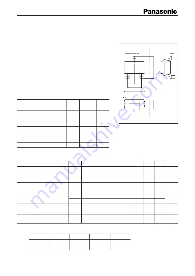
Unit: mm
2.1
±
0.1
1.3
±
0.1
0.3
+0.1
–0.0
2.0
±
0.2
1.25
±
0.10
(0.425)
1
3
2
(0.65) (0.65)
0.2
±
0.1
0.9
±
0.1
0 to 0.1
0.9
+0.2 –0.1
0.15
+0.10
–0.05
5˚
10˚
Note) 1. Measuring methods are based on JAPANESE INDUSTRIAL STANDARD JIS C 7030 measuring methods for transistors.
2. *: Rank classification
Rank
Q
R
S
No rank
h
FE1
160 to 260
210 to 340
290 to 460
160 to 460
Marking symbol
ZQ
ZR
ZS
Z
Product of no-rank is not classified and have no marking symbol for rank.
Marking Symbol: Z
1: Base
2: Emitter
3: Collector
EIAJ: SC-70
SMini3-G1 Package
This product complies with the RoHS Directive (EU 2002/95/EC).


