Transistors
1
Publication date: August 2004
SJC00313AED
2SD1938(F)
Silicon NPN epitaxial planar type
For low-voltage output amplification
For muting
For DC-DC converter
■
Features
•
Low ON resistance R
on
•
High forward current transfer ratio h
FE
•
Mini type package, allowing downsizing of the equipment and
automatic insertion through the tape packing
■
Absolute Maximum Ratings
T
a
=
25
°
C
Parameter
Symbol
Rating
Unit
Collector-base voltage (Emitter open)
V
CBO
50
V
Collector-emitter voltage (Base open)
V
CEO
20
V
Emitter-base voltage (Collector open)
V
EBO
25
V
Collector current
I
C
300
mA
Peak collector current
I
CP
500
mA
Collector power dissipation
P
C
200
mW
Junction temperature
T
j
150
°
C
Storage temperature
T
stg
−
55 to
+
150
°
C
Parameter
Symbol
Conditions
Min
Typ
Max
Unit
Collector-emitter voltage (Base open)
V
CEO
I
C
=
1 mA, I
B
=
0
20
V
Base-emitter voltage
V
BE
V
CE
=
2 V, I
C
=
4 mA
0.6
V
Collector-base cutoff current (Emitter open)
I
CBO
V
CB
=
50 V, I
E
=
0
0.1
µ
A
Emitter-base cutoff current (Collector open)
I
EBO
V
EB
=
25 V, I
C
=
0
0.1
µ
A
Forward current transfer ratio
*1
h
FE
V
CE
= 2 V, I
C
= 4 mA
500
2 500
Collector-emitter saturation voltage
V
CE(sat)
I
C
=
30 mA, I
B
=
3 mA
0.1
V
Transition frequency
f
T
V
CB
=
6 V, I
E
=
−
4 mA, f
=
200 MHz
80
MHz
Collector output capacitance
C
ob
V
CB
=
10 V, I
E
=
0, f
=
1 MHz
7
pF
(Common base, input open circuited)
ON resistance
*2
R
on
1.0
Ω
■
Electrical Characteristics
T
a
=
25
°
C
±
3
°
C
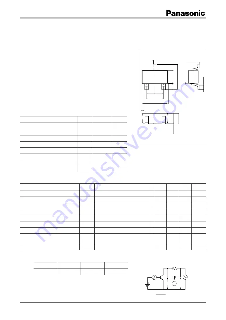
Unit: mm
Note) 1. Measuring methods are based on JAPANESE INDUSTRIAL STANDARD JIS C 7030 measuring methods for transistors.
2. *1: Rank classification
*2: R
on
Measuremet circuit
Rank
S
T
No rank
h
FE
500 to 1 500
800 to 2 500
500 to 2 500
V
V
1 k
Ω
R
on
=
V
B
×
1 000 (
Ω
)
V
A
−
V
B
f
=
1 kHz
V
=
0.3 V
V
B
I
B
=
1 mA
V
A
1: Base
2: Emitter
3: Collector
EIAJ: SC-59
JEDEC: SOT-346
Mini3-G1 Package
Marking symbol: 3W
0.40
+0.10
–0.05
(0.65)
1.50
+0.25 –0.05
2.8
+0.2 –0.3
2
1
3
(0.95) (0.95)
1.9
±
0.1
2.90
+0.20
–0.05
0.16
+0.10
–0.06
0.4
±
0.2
5˚
10˚
0 to 0.1
1.1
+0.2 –0.1
1.1
+0.3 –0.1
Product of no-rank classification is not marked.
This product complies with the RoHS Directive (EU 2002/95/EC).