background image

Revised

User’s Guide

for Evaluation Board

Total Pages

Page

1

14

EVB-NN30312A

Part No.

Part No.

Industrial Devices Company, Panasonic Corporation

Industrial Devices Company

Panasonic Corporation

Regulations
No.

312A805E

Tentative

The product specifications described in this book are subject to change without 
notice for the product which is currently under development. At the final stage of 
your design, purchasing, or use of the product, therefore, ask for the most up-to-
date Product Standards in advance to make sure that the latest specifications satisfy 
your requirements.

2012-04-17

Summary of Contents for EVB-NN30312A

Page 1: ...n Regulations No 312A805E Tentative The product specifications described in this book are subject to change without notice for the product which is currently under development At the final stage of your design purchasing or use of the product therefore ask for the most up to date Product Standards in advance to make sure that the latest specifications satisfy your requirements 2012 04 17 ...

Page 2: ...o 312A805E 2012 04 17 Contents 1 Introduction 1 1 Overview 3 1 2 Features 3 1 3 Typical Applications 3 1 4 Package 3 1 5 Type 3 1 6 Block Diagram 4 2 Evaluation Board 2 1 Appearance 5 2 2 Jumper setup 6 3 Schematic 7 4 Test Setup 4 1 Main Test Points and Jumpers 8 4 2 Output Voltage Setpoint 9 5 Bill of Materials 10 6 Board Layout 11 Usage Notes 14 ...

Page 3: ...DC Step Down Regulator circuit that employs the hysteretic control system Integrated Two 9mΩ Typ MOSFETs for high efficiency Switchable FCCM continuous SKIP discontinuous mode Input Voltage Range 4 5V TBD 30V TBD Output Voltage Range 0 75V TBD 5 5V TBD Built in 0 6V 1 TBD Reference Voltage Selectable Switching Frequency 250kHz 750kHz 1250kHz Adjustable Soft Start Low Operating and Standby Quiescen...

Page 4: ...ic Corporation Regulations No 312A805E 2012 04 17 1 6 Block Diagram Figure 1 Block Diagram Driver Control Logic CTL VREF SS VREG Soft Start VREF Soft Start VOUT MODE VFB VREG FSEL EN SS AVIN PGOOD BST PVIN LX PGND AGND AVIN PVIN VREG ON OFF VOUT Note The parameters above is subject to change without notice for improvement ...

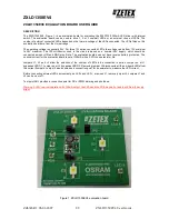
Page 5: ... 2012 04 17 2 Evaluation Board 2 1 Appearance Jumper for EN Please see the next page for further details about jumper setup Jumper for MODE Jumper for FSEL Jumper for PGOOD GND PVIN Force PVIN Sense VOUT Force VOUT Sense ー ー V GND Load A ー ー V Figure 2 Appearance of Evaluation Board Note The parameters above is subject to change without notice for improvement ...

Page 6: ...FCCM SKIP SKIP Table 3 J MODE Control modes J MODE J MODE Table 4 J FSEL Control SW frequency Table 5 J PGOOD Control the Voltage PGOOD pin pulled up to Jumper Status enable disable disable Table 2 J EN Control enable disable J EN J EN Jumper Frequency 250kHz 750kHz 1250kHz J FSEL J FSEL Jumper Pull up to VREG open V EXT J PGOOD J PGOOD J EN J MODE J FSEL J PGOOD Figure 3 Appearance of J EN J MODE...

Page 7: ...T1 C DCDCOUT2 C DCDCOUT3 C DCDCOUT4 C DCDCOUT5 R FB4 R FB1 SL_PVIN R AVIN To AVIN To PVIN LX BST MODE AGND AVIN EN VREG VFB VOUT SS PGOOD AGND PVIN C PVIN1 C PVIN2 PVIN C PVIN3 C PVIN4 C PVIN5 C PVIN6 C AVIN1 C AVIN2 C BST AVIN R FB5 D LX1 D LX2 D BST J MODE VREG J PGOOD J EN VREG J FSEL C FSEL R FB7 FB SUB R3 R2 C1 R1 C3 FB SUB C2 DCDCOUT V EXT R PG PGOOD CAP_GND PVIN AVIN C SS SS EN V EN C VREG ...

Page 8: ...to EN pin Jumpers J EN V EN 3 pin headers for enable of NN30312A Connect EN to GND to disable to V EN to enable J MODE VREG 3 pin headers to choose mode Connect MODE to GND to choose SKIP mode to VREG to choose FCCM mode J FSEL 3 pin headers to choose frequency Connect FSEL to GND to choose 1250kHz open to choose 750kHz to VREG to choose 250kHz J PGOOD open 3 pin headers for pull up of PGOOD Conne...

Page 9: ...f R FB1 R FB4 for a specific output value can be calculated using Equation 1 For output voltage from 0 75V to 5 5V Table 8 lists the R FB1 R FB4 values for some common output voltage Vout R FB3 R FB4 R FB1 R FB2 R FB3 R FB4 x 0 6 1 Output Voltage V R FB1 k ohm R FB2 k ohm R FB3 k ohm R FB4 k ohm 1 00 1 0 0 1 5 0 1 05 1 2 0 1 6 0 1 20 1 5 0 1 5 0 1 80 1 0 1 0 1 0 0 2 50 4 7 1 0 1 8 0 3 30 3 3 1 2 1...

Page 10: ... J PGOOD L LX 1 1 0uH Inductor 13A 7 1mΩ 7 1 6 5 mm TDK SPM6530 1R0M120 R1 R2 R3 R AVIN 1 0 Resistor Chip 0 1W 0603 Panasonic ERJ3GEY0R00V R FB1 2 1 3 3k Resistor Chip 0 1W 1 0603 Panasonic ERJ3EKF3301V R FB2 2 1 1 2k Resistor Chip 0 1W 1 0603 Panasonic ERJ3EKF1201V R RB3 2 1 1 0k Resistor Chip 0 1W 1 0603 Panasonic ERJ3EKF1001V R FB4 2 1 0 Resistor Chip 0 1W 0603 Panasonic ERJ3GEY0R00V R FB6 1 0 ...

Page 11: ...onic Corporation Regulations No 312A805E 2012 04 17 The board layout for the evaluation board is shown in Figure 5 through Figure 10 Figure 5 Top Layer with silk screen Top View Figure 6 Bottom Layer with silk screen Bottom View 6 Board Layout Note The parameters above is subject to change without notice for improvement ...

Page 12: ...d Revised Total Pages Page Tentative Industrial Devices Company Panasonic Corporation Regulations No 312A805E 2012 04 17 Figure 7 Top Layer Top View Figure 8 Layer 2 Top View Note The parameters above is subject to change without notice for improvement ...

Page 13: ...Revised Total Pages Page Tentative Industrial Devices Company Panasonic Corporation Regulations No 312A805E 2012 04 17 Figure 9 Layer 3 Top View Figure 10 Bottom Layer Top View Note The parameters above is subject to change without notice for improvement ...

Page 14: ...ying power otherwise damage might happen due to problems such as a solder bridge between the pins of the semiconductor device Also perform a full technical verification on the assembly quality because the same damage possibly can happen due to conductive substances such as solder ball that adhere to the LSI during transportation 5 Take notice in the use of this product that it might break or occas...

Page 15: ...on with your using the products described in this book for any special application unless our company agrees to your using the products in this book for any special application 4 The products and product specifications described in this book are subject to change without notice for modification and or im provement At the final stage of your design purchasing or use of the products therefore ask fo...

Reviews: