background image

© Panasonic Corporation 2011 Unauthorized copy-
ing and distribution is a violation of law.

ORDER NO. VM1104033CE

B27

Dual Camera

Model No.

HX-DC1P
HX-DC1PC
HX-DC1PU
HX-DC1EB
HX-DC1EC
HX-DC1EE
HX-DC1EF
HX-DC1EG
HX-DC1GA
HX-DC1GC
HX-DC1GD
HX-DC1GK
HX-DC1GN
HX-DC1GT

Vol. 1

Colour
(H)...........Gray Type
(W)..........White Type (except EB/EC)
(P)...........Pink Type (except PU/EB/EC/EE)
(K)...........Black Type (only EB)
(R)...........Red Type (only EB)

Summary of Contents for HX-DC1EB

Page 1: ...RDER NO VM1104033CE B27 Dual Camera Model No HX DC1P HX DC1PC HX DC1PU HX DC1EB HX DC1EC HX DC1EE HX DC1EF HX DC1EG HX DC1GA HX DC1GC HX DC1GD HX DC1GK HX DC1GN HX DC1GT Vol 1 Colour H Gray Type W White Type except EB EC P Pink Type except PU EB EC EE K Black Type only EB R Red Type only EB ...

Page 2: ...del 8 3 5 Formatting 9 4 Specifications 10 5 Location of Controls and Components 12 6 Service Fixture Tools 14 6 1 When Replacing the Main P C B 14 7 Disassembly and Assembly Instructions 15 7 1 Disassembly Flow Chart 15 7 2 PCB Location 15 7 3 Disassembly Procedure 16 8 Measurements and Adjustments 25 8 1 Electric Adjustment 25 9 Block Diagram 27 9 1 Overall Block Diagram 27 9 2 Interconnection D...

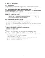
Page 3: ...exposed to shock hazards 1 2 Leakage Current Cold Check 1 Unplug the AC cord and connect a jumper between the two prongs on the plug 2 Measure the resistance value with an ohmmeter between the jumpered AC plug and each exposed metal lic cabinet part on the equipment such as screwheads connectors control shafts etc When the exposed metal lic part has a return path to the chassis the reading should ...

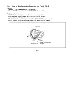
Page 4: ...ing Procedure 1 Refer to the disassemble procedure and Remove the necessary parts unit 2 Put the insulation tube onto the lead part of Resistor ERG5SJ102 1kΩ 5W an equivalent type of resistor may be used 3 Put the resistor between both terminals of capacitor on FLASH P C B for approx 5 seconds 4 After discharging confirm that the capacitor voltage is lower than 10V using a voltmeter Fig F1 ...

Page 5: ...ly a grounded tip soldering iron to solder or unsolder ES devices 4 Use only an antistatic solder removal device Some solder removal devices not classified as antistatic ESD protected can generate electrical charge sufficient to damage ES devices 5 Do not use freon propelled chemicals These can generate electrical charges sufficient to damage ES devices 6 Do not remove a replacement ES device from...

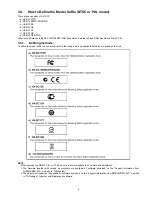
Page 6: ...OTE This Lithium battery is a critical component It must never be subjected to excessive heat or discharge It must therefore only be fitted in requirement designed specifically for its use Replacement batteries must be of same type and manufacture They must be fitted in the same manner and location as the original battery with the correct polarity contacts observed Do not attempt to re charge the ...

Page 7: ...free solder it should be well molten and mixed with the original lead free solder Remove the remaining lead free solder on the P C B cleanly for soldering of the new IC Since the melting point of the lead free solder is higher than that of the normal lead solder it takes the longer time to melt the lead free solder Use the soldering iron more than 70W equipped with the temperature control after se...

Page 8: ... the model suffix to be serviced refer to the rating label and caution label which are putted on the Unit NOTE After replacing the MAIN P C B or IC102 be sure to achieve update the Firmware and adjustment 1 The firmware together with version up procedure are available at software download on the Support Information from NWBG VDBG AVC web site in TSN system 2 The adjustment instruction is available...

Page 9: ...9 3 5 Formatting ...

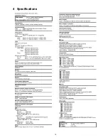
Page 10: ...10 4 Specifications ...

Page 11: ...11 ...

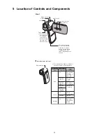
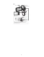
Page 12: ...h longer than 5 5 mm 0 22 may damage the camera About the status indicator The status indicator lights or flashes to show the camera s operating status Status indicator status Camera status Color Lit flashing Red Lit Accessing built in memory or SD card Flashing Faster Battery charge error Flashing Fast Self timer is operating Flashing Slow Battery is charging Flashing Slower Green Lit USB connect...

Page 13: ...ooting button button button SET button REC button Video recording button MENU button ZOOM RANGE button Hand strap eyelet HDMI terminal USB AV terminal Operation pad During recording zoom photography W T During playback volume adjustment image magnification playback display switching ...

Page 14: ...re and adjustment 1 The firmware together with version up procedure are available at software download on the Support Information from NWBG VDBG AVC web site in TSN system 2 The adjustment instruction is available at software download on the Support Information from NWBG VDBG AVC web site in TSN system together with Maintenance software ...

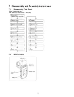
Page 15: ...15 7 Disassembly and Assembly Instructions 7 1 Disassembly Flow Chart This is a disassembling chart When assembling perform this chart conversely 7 2 PCB Location ...

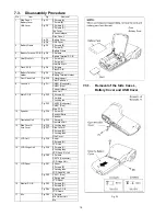
Page 16: ...nging part Front Case Unit 8 Lens Unit Fig D11 CN901 Connector CN951 Flex 2 Lens Holders Lens Unit 9 Main P C B Fig D12 2 Screws J 2 Solders 1 Locking tab Fig D13 CN103 Connector CN301 Flex Main P C B 10 Speaker Fig D14 1 Screw K Speaker Earth Speaker 11 Operation Unit Fig D15 1 Screw L Operation Unit 12 Side Cover R Grip Cover Fig D16 4 Locking tabs Fig D17 Side Cover R 2 Screws M 3 Locking tabs ...

Page 17: ...17 Fig D2 Fig D3 ...

Page 18: ...18 Fig D4 7 3 2 Removal of the Battery Frame Fig D5 7 3 3 Removal of the Battery Terminal P C B Fig D6 ...

Page 19: ...19 7 3 4 Removal of the Heat Sink Left Fig D7 7 3 5 Removal of the Flash P C B Unit Fig D8 ...

Page 20: ...20 7 3 6 Removal of the Battery Terminal Holder Fig D9 7 3 7 Removal of the Front Case Unit Fig D10 7 3 8 Removal of the Lens Unit Fig D11 ...

Page 21: ...21 7 3 9 Removal of the Main P C B Fig D12 Fig D13 7 3 10 Removal of the Speaker Fig D14 ...

Page 22: ...22 7 3 11 Removal of the Operation Unit Fig D15 7 3 12 Removal of the Side Cover R and Grip Cover Fig D16 Fig D17 ...

Page 23: ...23 7 3 13 Removal of the LCD Unit Fig D18 7 3 14 Removal of the LCD Hinge Unit Fig D19 Fig D20 7 3 15 Removal of the LCD Panel Fig D21 ...

Page 24: ...24 Fig D22 7 3 16 Removal of the Monitor P C B Fig D23 Fig D24 7 3 17 Removal of the Mic Fig D25 ...

Page 25: ... with PC Connection method of the main unit and an exclusive adjustment jig as follows 8 1 1 Adjustment Procedure Connect the main unit to PC with USB The adjustment instruction is available at Software download on the Support Information from NWBG VDBG AVC web site in TSN System Figure of connection Figure of image when adjustment Part Number of jig Only a necessary jig mentions it in setup of el...

Page 26: ...ock of the Lightbox Refer to following Fig for datailes Adjustment Items Adjustment item as follows The adjustment instruction is available at Software download on the Support Information from NWBG VDBG AVC web site in TSN System ...

Page 27: ...E DETECT PANEL_OPEN X3001 32 768KHz IC501 SWITCHING CONTROL USB CHARGE PWA BLOCK POWER MANAGEMENT RTC CEC HPD DDC_ SCL SDA CN801 CN110 USB HOST CONTROL HDMI AUDIO CODEC SPEAKER SP SP TMDS_CLK TMDS_DATA0 TMDS_DATA1 TMDS_DATA2 I2C_ SDA SCL PON LCD EN CK SD BACKUPBAT MIC_ L R LCD AN CA STROBE STROBE CHARGE CONTROL USB_SUSPWR BATCHGOFF USB_HPWR LITHIUM ION BATTERY 700mAh min LMCLK LCDD 0 7 LCD HD VD U...

Page 28: ...38 GND 39 GND 40 GND 41 AGND 42 AGND 43 VAAPIX 44 VAAPIX JW185 1 SP JW186 1 SP CN541 1 GND 2 GND 3 GND 4 GND 5 UNREGST 6 UNREGST 7 UNREGST 8 BAT_TEMP 9 GND 10 CHG 11 ZCHGDONE 12 FLCTL 13 VDD3 14 15 BAT 16 BAT 17 BAT 18 BAT 19 BAT 20 BAT 21 BAT 22 BAT 23 BAT 24 BAT 25 BAT 26 BAT 27 BAT SY 28 GND 29 GND 30 GND 31 GND 32 GND 33 GND 34 GND 35 GND 36 GND 37 GND 38 GND 39 GND 40 GND GRAY JW544 1 GND JW5...

Page 29: ...5412 Q5402 POWER FILTER OSCILLATION TRANSFORMER BLOCK RECTIFIER CIRCUIT EMISSION CONTROL CIRCUIT TRIGGER CIRCUIT LIGHT EMITTING ELEMENT XENON TUBE CHARGING CIRCUIT LIGHT EMISSION CIRCUIT 4 OSCILLATION CIRCUIT IGBT DRIVER CHARGE MONITOR CIRCUIT IC541 10 6 9 5 FLASH CHARGE MODEL HX DC1 BLOCK DIAGRAM FLASH UNREGST ...

Page 30: ...25NUX QBD4225NUX P IC541 1 PGND 2 IGBT_OUT 3 GND 4 VC 5 VCC 6 START 7 IGBT_IN 8 RADJ 9 FULL 10 SW Z1 P S F TTRN 0522H 003 T 1AV4L17B0651G T5401 1 2 3 4 5 TIG065E8 H Q5402 1 2 3 4 5 6 7 8 CN541 1 GND 2 GND 3 GND 4 GND 5 UNREGST 6 UNREGST 7 UNREGST 8 BAT_TEMP 9 GND 10 CHG 11 ZCHGDONE 12 FLCTL 13 VDD3 14 GND 15 BAT 16 BAT 17 BAT 18 BAT 19 BAT 20 BAT 21 BAT 22 BAT 23 BAT 24 BAT 25 BAT 26 BAT 27 BAT SY...

Page 31: ...3 D2 14 D1 15 D0 16 GND 17 VDD 18 DVDD 19 V1 20 V2 21 V3 22 V4 23 VDD2 24 V5 25 V6 26 VDD3 27 VDD5 28 V7 29 V8 30 VGH 31 VGL 32 AGND 33 FRP 34 COMDC 35 VCAC 36 DRV 37 VLED 38 FB 39 VCOM Z1 Z2 0 RB171 1 2 0 RB171 3 4 0 RB171 5 6 0 RB171 7 8 0 RB172 3 4 0 RB172 1 2 0 RB172 5 6 0 RB172 7 8 0 1 16Z R1705 CN174 1 GND 2 VDD3 3 HINGE 4 LCDD0 5 LCDD1 6 LCDD2 7 LCDD3 8 LCDD4 9 LCDD5 10 LCDD6 11 LCDD7 12 GN...

Page 32: ...W352 1 MODEL HX DC1 CIRCUIT DIAGRAM SW SW T1 31800 SG515 JPA TO MONITOR JW187 TO MONITOR JW188 ZHINGE JW652 1 BAT_TEMP JW651 1 GND DC JW653 1 BAT DC CN651 1 DC 2 T 3 DC RED YELLOW BLUE BATTERY TERMINAL T2 31800 SG515 JPA TO FLASH JW522 TO FLASH JW523 TO BATTERY TO FLASH JW521 MODEL HX DC1 CIRCUIT DIAGRAM BATTERY TERMINAL ...

Page 33: ...C5401 C5434 C5435 C5436 R5424 R5425 R5432 R5434 R5435 R5436 R5439 IC541 CL506 Q5402 C5410 CL545 CL548 D5402 R5422 F5009 RB541 T5401 JW521 JW522 JW523 JW541 JW542 JW543 JW544 SIDE B SG513 SG515 SG517 ST1 K9500AB 1 40 20 21 CL507 CL508 CL549 CL551 CL552 CL560 CL561 CL563 CN541 MODEL HX DC1 CIRCUIT BOARD FLASH SIDE A SIDE B ...

Page 34: ...26 C1727 C1728 C1729 R1701 R1702 R1703 R1704 R1705 C1730 R1725 R1726 VA181 VA182 C1851 C1852 C1853 C1854 C1855 C1856 C1857 C1860 C1866 C1869 C1870 C1871 C1872 C1873 R1851 R1852 R1853 R1854 R1855 R1856 R1857 R1858 R1859 R1860 R1861 R1863 R1864 R1866 R1867 R1868 R1869 R1870 R1874 R1875 C1867 C1868 C1731 C1732 C1773 J W 1 8 1 J W 1 8 2 J W 1 8 3 J W 1 8 4 JW187 JW188 IC185 IC186 RB171 RB172 RB185 Z63...

Page 35: ...rminal P C B MODEL HX DC1 CIRCUIT BOARD SW and BATTERY TERMINAL SIDE A SIDE B RD WT S A SG513 TB1 K9500BB S B BL YL RD SG513 K950 TB2 0DB S3501 CN651 JW351 JW352 J W 6 5 1 J W 6 5 2 JW653 SW P C B SIDE A SIDE B BATTERY TERMINAL P C B ...

Page 36: ...36 12 Exploded View and Replacement Parts List 12 1 Exploded Views ...

Page 37: ...37 ...

Page 38: ...38 ...

Page 39: ...3034085500 C CAPACITOR 2 2U 16V 1 C1730 VU4034615417 C CAPACITOR 4 7U K 10V 1 C1773 VU3033818109 C CAPACITOR 1U 6 3V 1 C1867 VU3033846419 C CAPACITOR 4 7U K 6 3V 1 C1868 VU3033846419 C CAPACITOR 4 7U K 6 3V 1 C1871 VU3033469816 C CAPACITOR 0 047U K 10V 1 C1872 VU3033469816 C CAPACITOR 0 047U K 10V 1 C1873 VU3033380309 C CAPACITOR 0 1U 10V 1 CN171 VU6451010858 CONNECTOR 39P 1 CN174 VU6451042798 CON...

Page 40: ...INGE UNIT 1 W 113 VU6361537322 LCD HINGE UNIT 1 R 114 VU6361517874 CAUTION LABEL 1 P PC PU EG EF EC EB GC EE GN GA 114 VU6361517898 CAUTION LABEL 1 GT Safety Ref No Part No Part Name Description Pcs Remarks 114 VU6361517904 CAUTION LABEL 1 GD 114 VU6361517911 CAUTION LABEL 1 GK 115 VU6361517881 CAUTION LABEL 1 PC 116 VU6361540131 SIDE COVER R 1 H 116 VU6361503891 SIDE COVER R 1 P 116 VU6361503907 ...

Page 41: ...H 1 PU 220 VQT3M93 OPERATING INSTRUCTIONS GERMAN TURKISH 1 EG 220 VQT3M94 OPERATING INSTRUCTIONS ITALIAN DUTCH 1 EG 220 VQT3Q26 OPERATING INSTRUCTIONS FRENCH 1 EF 220 VQT3M96 OPERATING INSTRUCTIONS PORTGUESE SPANISH 1 EC 220 VQT3M97 OPERATING INSTRUCTIONS SWEDISH DANISH 1 EC 220 VQT3N01 OPERATING INSTRUCTIONS ENGLISH 1 EB 220 VQT3Q27 OPERATING INSTRUCTIONS THAI 1 GA 220 VQT3N03 OPERATING INSTRUCTI...

Reviews: