background image

© Panasonic Corporation 2010. All rights reserved.
Unauthorized copying and distribution is a violation
of law.

PSG1003045CE

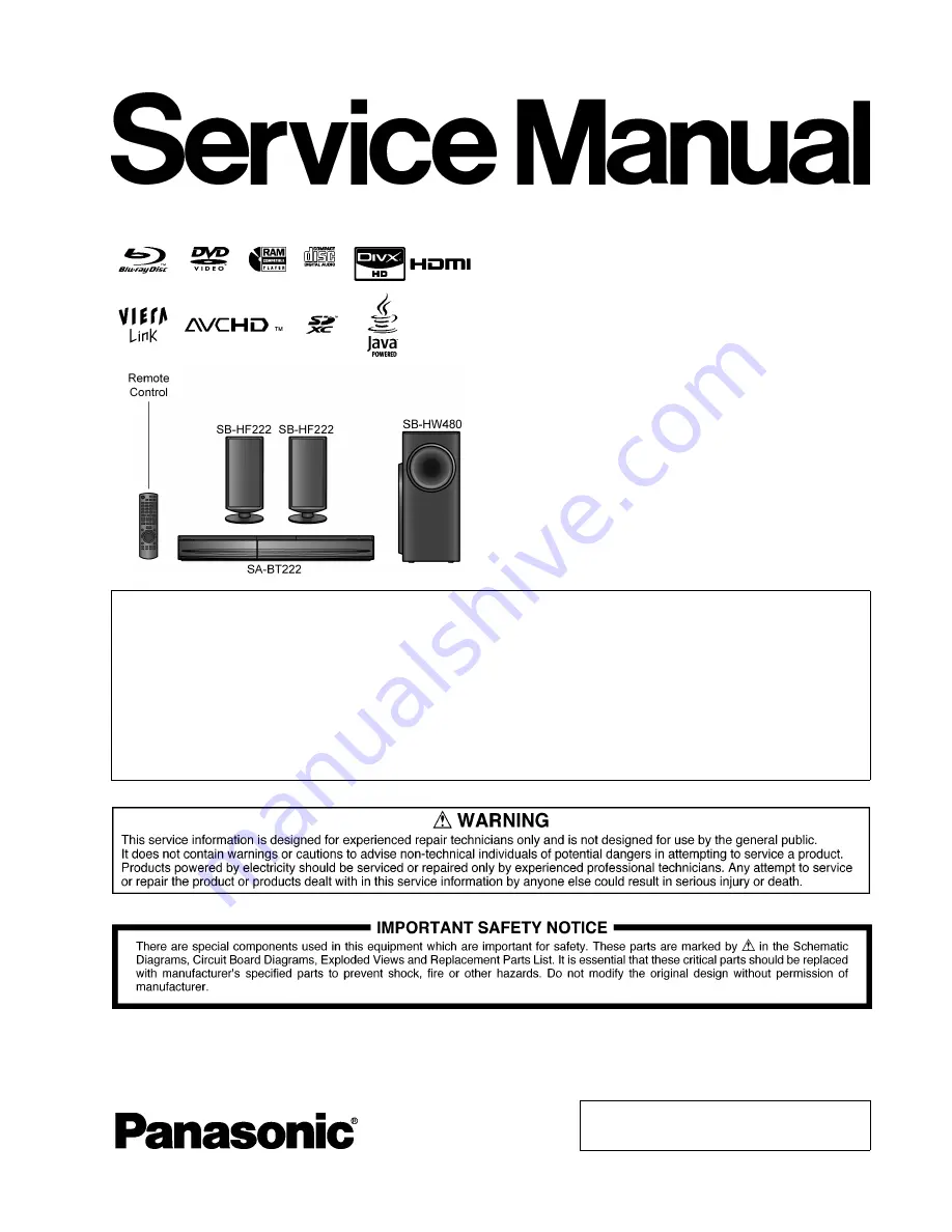
Blu-ray Disc Home Theater Sound System

Model No.

SA-BT222EB
SA-BT222EG

Volume 1

Product Color:  (K)...Black Type

TABLE OF CONTENTS

PAGE

PAGE

Notes: 1) These model’s BD Drive/Main P.C.B. Assembly are:- 
                                    - RFKNBT222EBA (For EB); 
                                    - RFKNBT222EGA (For EG).
            2) Please refer to the original service manual for:
                • Speaker system SB-BT222EG-K, Order No: PSG1003048CE.

Caution:
Pairing of BD Drive and Main P.C.B. as “BD Drive & Main P.C.B. Assembly” have to be replaced together. If
either BD Drive or Main P.C.B. is changed, BD Drive unit has to carry out re-adjustment due to alignment
data for BD Drive Unit is stored in the Main P.C.B.

Summary of Contents for SA-BT222EB

Page 1: ... Notes 1 These model s BD Drive Main P C B Assembly are RFKNBT222EBA For EB RFKNBT222EGA For EG 2 Please refer to the original service manual for Speaker system SB BT222EG K Order No PSG1003048CE Caution Pairing of BD Drive and Main P C B as BD Drive Main P C B Assembly have to be replaced together If either BD Drive or Main P C B is changed BD Drive unit has to carry out re adjustment due to alig...

Page 2: ...52 10 12 Disassembly of iPod iPhone P C B 54 10 13 Replacement of DVD Lid Unit 55 10 14 Disassembly of Front Shield Plate Unit 57 10 15 Disassembly of BD Drive 58 10 16 Disassembly of Main P C B 64 10 17 Disassembly of D Amp P C B 65 10 18 Replacement of Digital Amplifier IC IC5100 67 10 19 Disassembly of Power P C B 68 10 20 Disassembly of SMPS P C B 68 10 21 Replacement of Switching Regulator IC...

Page 3: ...ation resistance test to prevent the customer from being exposed to a shock hazard 1 1 2 LEAKAGE CURRENT HOT CHECK 1 Plug the AC cord directly into the AC outlet Do not use an isolation transformer for this check 2 Connect a 1 5kΩ 10 watts resistor in parallel with a 0 15µF capacitors between each exposed metallic part on the set and a good earth ground such as a water pipe as shown in Figure 1 3 ...

Page 4: ... damage if for example the positive and negative speaker connection wires are shorted or if speaker systems with an impedance less than the indicated rated impedance of the amplifier are used If this occurs follow the procedure outlines below 1 Turn off the power 2 Determine the cause of the problem and correct it 3 Turn on the power once again after one minute Note When the protection circuitry f...

Page 5: ...A2 RFAX0024 AC CORD UNIT EG A2 RFAX1022 AC CORD UNIT EB A3 VQT2S24 O I BOOK Fr EG A3 VQT2S25 O I BOOK Ge It EG A3 VQT2S26 O I BOOK Sp Du EG A3 VQT2S27 O I BOOK Da Sw EG A3 VQT2S28 O I BOOK En EB PCB5 REPX0803P SMPS P C B RTL PCB6 REPX0803P AC INLET P C B RTL PCB9 RFKNBT222EBA BD DRIVE MAIN P C B ASS Y EB PCB9 RFKNBT222EGA BD DRIVE MAIN P C B ASS Y EG DZ5701 ERZV10V511CS ZNR L5702 ELF21N015A LINE F...

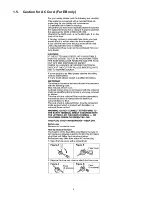
Page 6: ...6 1 5 Caution for AC Cord For EB only ...

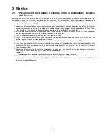
Page 7: ...f the assembly 3 Use only a grounded tip soldering iron to solder or unsolder ES devices 4 Use only an anti static solder removal device Some solder removal devices not classified as anti static ESD protected can generate electrical charge sufficient to damage ES devices 5 Do not use freon propelled chemicals These can generate electrical charges sufficient to damage ES devices 6 Do not remove a r...

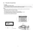
Page 8: ... output radiation power from pickup 100 µW VDE Laser radiation from the pickup unit is safety level but be sure the followings 1 Do not disassemble the pickup unit since radiation from exposed laser diode is dangerous 2 Do not adjust the variable resistor on the pickup unit It was already adjusted 3 Do not look at the focus lens using optical instruments 4 Recommend not to look at pickup lens for ...

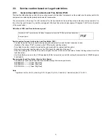
Page 9: ...is used Definition The letter of PbF is printed on the PCB using the lead free solder To put lead free solder it should be well molten and mixed with the original lead free solder Remove the remaining lead free solder on the PCB cleanly for soldering of the new IC Since the melting point of the lead free solder is higher than that of the normal lead solder it takes the longer time to melt the lead...

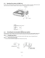
Page 10: ...wn prevention Some devices such as the DVD player use the optical pickup laser diode and the optical pickup will be damaged by static electric ity in the working environment Proceed servicing works under the working environment where grounding works is completed 2 4 1 1 Worktable grounding 1 Put a conductive material sheet or iron sheet on the area where the optical pickup is placed and ground the...

Page 11: ... will be followed by supplement service manual to be filed with the original ser vice manual BD Drive Digital Circuitries 1 This service manual does not contain the following information due to the impossibility of servicing at component level Schematic Diagram Block Diagram Electrical Replacement Partlist for individual of Digital Circuitries 2 The following category are recycle module part Pleas...

Page 12: ...ality should be seen in the picture sound or operation 6 If a problem is caused by a BD Video disc VCD DVD R DVD Video Audio CD or MP3 playback the test disc No abnormality should be seen in the picture sound or operation 7 After checking and making repairs upgrade the firmware to the latest version Make sure that UPD OK appears in the FL displays UNSUPPORT display means the unit is already update...

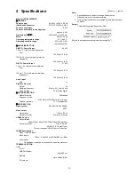
Page 13: ... Digital OFM TUNER SECTION Present Memory 30 Stations Frequency range 87 50 MHz to 108 00 MHz 50 kHz step Antenna terminals 75 Ω unbalanced OVIDEO SECTION Signal system PAL 625 50 PAL 525 60 NTSC Video output Output level 1 0 Vp p 75 Ω Output connector Pin jack 1 system HDMI AV output Output format 480p 525p 1080i 1125i 720p 750p 1080p 1125p Output connector Type A 19 pin HDMI V 1 4 Content Type T...

Page 14: ...14 ...

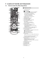
Page 15: ...15 5 Location of Controls and Components 5 1 Remote Control Key Button Operations ...

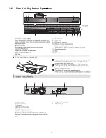
Page 16: ...16 5 2 Main Unit Key Button Operations ...

Page 17: ...17 5 3 Using BD LIVE BONUSVIEW in BD Video ...

Page 18: ...18 5 4 Using the iPod iPhone ...

Page 19: ...19 5 4 1 iPod iPhone Playback ...

Page 20: ...20 5 5 Speaker Connections ...

Page 21: ...21 5 6 Disc Playability ...

Page 22: ...22 ...

Page 23: ...23 5 7 SD USB Information ...

Page 24: ...24 5 8 File Extension Type Support MP3 JPEG DivX AVCHD MPEG2 files ...

Page 25: ...25 5 8 1 File Folders Structures ...

Page 26: ...2 When the power cannot be turned off 1 Press hold the POWER button to turn off the power forcibly then press hold SKIP FWD button on remote and OPEN CLOSE button on main unit for 5 seconds 6 1 2 Using service eject pin 1 Turn off the power and remove AC cord 2 Remove the Top Cabinet 3 Remove BD Drive 4 Insert Eject Pin JZJ0484 into the hole on the bottom of BD Drive and slide the eject Pin in the...

Page 27: ...s displayed for five seconds Same display as before execution When power on press STOP on main unit POWER on remote control When power is off press SKIP FWD on remote control OPEN CLOSE key on main unit simultaneously for 5 seconds or more Forced disc eject Removing a disc that cannot be ejected The tray will open and unit will shift to P off mode While Demonstration Lock is being set this Forced ...

Page 28: ...Progressive initialization The progressive setting is initialized to Inter lace The display before execution leaves When the power is on SS mode press STOP and PLAY simulta neously for 5 seconds Item FL display Key operation Mode name Description Front Key When the power is on press PLAY and OPEN CLOSE keys simultaneously for 5 seconds When the power is on press PLAY and OPEN CLOSE keys simultaneo...

Page 29: ...I or when there is a problem with the HDMI cable No display U73 display disappears when error has been solved by Power OFF ON of connecting equipment or by inserting removing of HDMI cable F99 Hang up Displayed when communication error has occurred between Main microprocessor and Timer microprocessor No display Displayed is left until the POWER key is pressed H19 Inoperative fan motor When inopera...

Page 30: ...or Code Diagnosis contents Description Monitor Display Automatic FL display SELF CHECK PLEASE WAIT UNFORMAT No PLAY The character indication flows sideways Error Code F61 The abnormalities In normal operation when DCDET2 goes Press STOP on main in an output or power to L Low Not during POWER OFF unit for next error supply circuit of condition F61 appears on FLDisplay POWER AMP for 1 second and PCO...

Page 31: ... by Timer is dis played on FL Details are described in 7 1 1 Self Diagno stic Functions If any error history dose not exist F00 is displayed Press 0 1 in service mode ROM Version Display 1 Region code displayed for 5 sec 2 Main firm version displayed for 5 sec 3 Timer firm version displayed for 5 sec 4 Drive firm version displayed for 5 sec 5 ROM correction version left displayed are version displ...

Page 32: ...ve Press 4 1 in service mode Item FL display Key operation Mode name Description Remote controller key Laser used time of BD DVD CD in Playback Recording mode is Counted BP BR DP DR CD 1 Blu ray Playback 2 Blu ray Recording 4 DVD Recording 5 CD 3 DVD Playback is the used time display in hour ...

Page 33: ...ds DD Day hh Hour mm Minute 3 Last drive error 1 2 is displayed for 5 seconds 00 Bad disc 03 Bad disc 04 Bad disc or drive malfunction 4 Last drive error 2 2 is displayed for five seconds 5 Error occurring disc type is dis played for 5 seconds Press 4 2 in service mode Item FL display Key operation Mode name Description Remote controller key DVDRW DDhhmm CDR NO CDRW DVDPR DVDPRW BDROM ...

Page 34: ...maker ID is displayed for 5 seconds 7 Factor of drive error hexadeci mal occurring is left displayed In case that the maker cannot be identified display is black out Item FL display Key operation Mode name Description Remote controller key ...

Page 35: ... the Last Drive Error Delete the Last Drive Error information stored on the DVD Drive Press 9 6 in service mode Delete the Error History Delete Error History information stored on the unit Press 9 7 in service mode Error code initialization Initialization of the last error code held by timer Write in F00 Press 9 8 in service mode Initialize Service Last Drive Error Error history and Error Codes st...

Page 36: ...b Short circuit between Pin 15 and pin 16 1c Short circuit between Pin 16 and 17 2 Power P C B 2a Check connection between Power P C B CN2916 CN2917 and SMPS P C B CN5802 CN5803 2b L2902 Open No input to IC2901 2c Faulty IC2901 No output voltage at pin 10 11 2d Faulty Q2902 Q2903 Regulator 2e L2907 open No DC 12v 2f L2908 op en No DC 5v 3 3 Check cable connection between main CN2004 and SMPS 4 4a ...

Page 37: ...37 8 1 1 SMPS P C B Figure 1 SMPS P C B FUSE F1 Photocouple PC5702 D5799 Switching IC IC5799 Switching IC IC5701 Transformer T5701 Rectifier D5802 ...

Page 38: ...38 8 1 2 Power P C B Fig 2 Power P C B CN2916 L2907 CN2917 L2908 Side B of Power P C B Side A of Power P C B IC2901 L2902 Q2903 Q2902 ...

Page 39: ...39 8 1 3 Main P C B Fig 3 Main P C B IC2302 LB2301 CN2004 ...

Page 40: ... Tools 9 1 Service Tools and Equipment Prepare service tools before process service position Service Tools Remarks SMPS P C B JW2 Main P C B CN2004 REXX1037 10P Cable Main P C B CN2006 D Amp P C B CN5402 RFKZBT230P 18P FFC ...

Page 41: ...g replacement of component parts please refer to the section of Replacement Parts List as described in the service manual Select items from the following indexes when disassembly or replacement are required Disassembly of Top Cabinet Disassembly of AC Inlet P C B Disassembly of Optical In P C B Disassembly of Rear Panel Disassembly of Front Panel Block Assembly Disassembly of Panel P C B Disassemb...

Page 42: ... BD Drive Power P C B 10 19 10 21 Switching Regulator IC IC5701 10 22 Rectifier Diode D5702 10 23 Regulator Diode D5802 10 24 Regulator Diode D5803 10 7 Front Panel Block 10 8 Panel P C B 10 14 Front Shield Plate Unit 10 9 Power Button P C B 10 12 iPod iPhone P C B 10 10 Cradle Lid 10 13 DVD Lid Unit 10 11 iPod Cradle Assembly 10 17 D Amp P C B 10 5 Optical In P C B ...

Page 43: ...43 10 2 Main Components and P C B Locations ...

Page 44: ...e of Top Cabinet Step 4 Slightly lift both side of Top Cabinet in an outward direc tion about 25 Step 5 Press down the catches one by one Caution To avoid shocked by electricity injured by high temperature DO NOT TOUCH electrical components when insert hand under the Top Cabinet Step 6 Remove Top Cabinet as arrow shown ...

Page 45: ...is pasted properly at Top Cabinet 10 4 Disassembly of AC Inlet P C B Refer to Disassembly of Top Cabinet Step 1 Remove 1 screw Step 2 Lift up the AC Inlet P C B from the rear panel Step 3 Desolder Red TL10 Black TL20 wires on AC Inlet P C B Step 4 Remove AC Inlet P C B 10 5 Disassembly of Optical In P C B Refer to Disassembly of Top Cabinet Step 1 Remove 2 screws ...

Page 46: ...s to release it from the locator as arrow 2 shown Step 5 Remove Optical In P C B 10 6 Disassembly of Rear Panel Refer to Disassembly of Optical In P C B Step 1 Lift up the Wire Clamper Step 2 Detach the fan unit connector CN5401 on D Amp P C B Step 3 Remove 7 screws Step 4 Release the tabs on both side of the Rear Panel in the direction of arrow Step 5 Remove Rear Panel ...

Page 47: ...FFC is dressed away from Power P C B when insertion to Main P C B Caution During assembling ensure that 15P FFC is dressed through Front Shield Step 3 Release the tabs on both side of the Front Panel Block Assembly in the direction of arrow Step 4 Release 3 tabs Caution Do not exert strong force when releasing the tabs Step 5 Detach the Front Panel Block Assembly 10 8 Dissassembly of Panel P C B R...

Page 48: ... at the connector CN6001 on Panel P C B Step 5 Remove Panel P C B Assembly of Panel P C B Step 1 Solder the 4P cable to the connector CN6001 on Panel P C B Step 2 Place the Panel P C B onto the Front Panel Step 3 Dress 22P FFC according to diagram shown Caution Ensure that it is properly located fully catched ...

Page 49: ...ton P C B Refer to Disassembly of Front Panel Block Assembly Disassembly of Power Button P C B Step 1 Remove 1 screw Step 2 Lift up the Power Button P C B Step 3 Desolder the 4P Cable H6803 on Power Button P C B Step 4 Remove Power Button P C B Assembly of Power Button P C B Step 1 Solder 4P cable at H6803 onto Power Button P C B ...

Page 50: ...o the Front Panel Caution Ensure that it is properly located seated prop erly Step 3 Fix 1 screw Step 4 Dress 4P cable in between Front Panel s ribs as shown Step 5 Dress 4P cable into Front Panel s ribs screw Boss according to diagram shown ...

Page 51: ...dle Lid Step 1 Release the Cradle Lid Spring by using a flat head screw driver in the direction of arrow Step 2 Slightly push the Cradle Lid inwards Step 3 Slightly lift up the Cradle Lid Step 4 Rotate the Cradle Lid about 45 according to the dia gram shown Step 5 Remove Cradle Lid 10 10 2 Assembly of Cradle Lid ...

Page 52: ...he Cradle Lid Shaft A into the Front Panel Slot A hole B Step 2 Slightly push the Cradle Lid inwards Step 3 Press the Cradle Lid downward Step 4 Fix the Cradle Lid Spring onto Cradle Lid s Shaft A 10 11 Disassembly of iPod Cradle Assembly Refer to Disassembly of Front Panel Block Assemb ley Step 1 Detach 15P FFC at the connector CN1002 on iPod ...

Page 53: ...p 4 Open the Cradle Lid Step 5 Lift up the iPod Cradle Assembly on both sides Step 6 Press to release iPod Cradle Assembly from Front Panel as arrow shown Step 7 Remove iPod Cradle Assembly Assembly of iPod Cradle Assembly Step 1 Fix the iPod Cradle Assembly to Front Panel ...

Page 54: ...ard when the iPod Cradle Assembly is fixed onto the Front Panel properly Step 3 Press the catch on the iPod Cradle Assembly Step 4 Fix 1 screw 10 12 Disassembly of iPod iPhone P C B Refer to Disassembly of iPod Cradle Assembly Step 1 Remove 2 screws Step 2 Remove iPod iPhone P C B ...

Page 55: ...ck Assembly 10 13 1 Disassembly of DVD Lid Unit Step 1 Push backward the Shaft B of the DVD Lid Unit in the direction of arrow Step 2 Push forward the Shaft B of the DVD Lid Unit in the direction of arrow Step 3 Lift the DVD Lid Spring at Shaft A in the direction of arrow Step 4 Move the Shaft A of the DVD Lid Unit in the direction of arrow Step 5 Remove DVD Lid Unit ...

Page 56: ...ep 1 Insert the DVD Lid Unit into the Front Panel as arrow shown Caution Ensure that Shaft A of DVD Lid Unit is fully inserted into Slot A of Front Panel Step 2 Locate DVD Lid Spring in between ribs of Front Panel Step 3 Insert the DVD Lid Unit Shaft B into the Front Panel Slot B as arrow shown ...

Page 57: ...isassembly of Front Panel Block Assembly Step 1 Remove 2 screws Step 2 Remove 1 screw Note Replace the Gaskets if broken Step 3 Slightly lift up the Front Shield Plate Unit to release 2 catches at both sides Step 4 Remove Front Shield Plate Unit Caution During assembling ensure that Front Shield is properly inserted fully fixed onto the Bottom Chassis ...

Page 58: ... and Main P C B as BD Drive Main P C B Assembly have to be replaced together If either BD Drive or Main P C B is changed BD Drive unit has to carry out re adjustment due to alignment data for BD Drive Unit is stored in the Main P C B Step 1 Detach 45P FFC at the connector P55001 on Main P C B Step 2 Detach 18P FFC at the connector P55002 on Main P C B Step 3 Remove 4 screws Step 4 Lift up to remov...

Page 59: ...ect Pin into the hole of the bottom side and slide it to the direction of arrow until it can be Step 2 Pull the Tray to the direction of arrow until it can be Step 3 Insert the Eject Pin into the hole of the Tray at 45 degrees and lean it to the direction of arrow with pushing the dotted point of the tray forward Then the one side of the tray is come off from the Drive Step 4 Insert the Eject Pin ...

Page 60: ...per Base Assembly Refer to Disassembly of Tray Refer to Disassembly of Pulley Gear Belt Step 1 Remove the Sheet Step 2 Disconnect the 3 FFCs Step 3 Remove the 2 Screws and the Angle Step 4 Peel off Coppery Sheet from FFC A and remove the Drive P C B Caution Though the Drive P C B is not supplied as replacement parts it must be removed for after disassem bling Step 5 Open the connector lock and dis...

Page 61: ...ssembly Refer to Disassembly of Tray Refer to Disassembly of Pulley Gear Belt Refer to Disassembly of Slide Cam Step 1 Remove the Mid Base and Driver Gear Step 2 Remove the Screw to remove the Loading Motor Step 3 Remove the Screw and remove the SW P C B with the Loading Motor Remove the 2 soldering points and remove the Loading Motor ...

Page 62: ...62 10 15 6 Applying of Grease ...

Page 63: ...63 10 15 7 Cleansing the Lens of Optical Pick Up Unit Refer to Disassembly of BD Drive Refer to Disassembly of Upper Base Assembly ...

Page 64: ...crews Step 2 Release the tab at the right side of Rear Panel in the direction of arrow Step 3 Detach 45P FFC at the connector P55001 on Main P C B Step 4 Detach 18P FFC at the connector P55002 on Main P C B Step 5 Detach 13P FFC at the connector CN2011 on Main P C B Step 6 Detach 18P FFC at the connector CN2006 on Main P C B Step 7 Lift up the Wire Clamper Step 8 Detach 10P cable at the connector ...

Page 65: ... Main P C B is seated properly at the locators 10 17 Disassembly of D Amp P C B Refer to Disassembly of Top Cabinet Assembly Step 1 Lift Up 2 Wire Clampers Step 2 Detach 3P Wire at the connector CN5401 on D Amp P C B Step 3 Detach 6P Cable at the connector CN5400 on D Amp P C B Step 4 Detach 18P FFC at the connector CN5402 on D Amp P C B ...

Page 66: ... using long nose plier Step 7 Remove 4 screws Step 8 Release the tab of the side of the Rear Panel in the direction of arrow Step 9 Remove D Amp P C B according to direction of arrow shown Caution During assembling ensure that D Amp P C B is seated properly at the locators ...

Page 67: ...lace it back during assembling Step 5 Desolder pins of Digital Amplifier IC IC5100 Step 6 Remove Digital Amplifier IC IC5100 10 18 2 Assembly of Digital Amplifier IC IC5100 Step 1 Mount the Digital Amplifier IC IC5100 onto the D Amp P C B Step 2 Solder pins of Digital Amplifier IC IC5100 Caution Ensure that the pins of Digital Amplifier IC IC5100 is positioned correctly on D Amp P C B before solde...

Page 68: ... follow to the illustration shown 10 19 Disassembly of Power P C B Refer to Disassembly of Top Cabinet Step 1 Release 2 catches Step 2 Remove Power P C B in the direction of arrow Caution During assembling ensure that Power P C B is properly inserted fully connected to SMPS P C B 10 20 Disassembly of SMPS P C B Refer to Disassembly of Power P C B Step 1 Release the 2 tabs at each side of the Front...

Page 69: ...rd Step 4 Lift up the Wire Clampers Step 5 Detach 6P Cable at the connector CN5400 on D Amp P C B Step 6 Detach 10P Cable at the connector CN2004 on Main P C B Caution During assembling ensure that 10P cable is bend down properly as diagram shown Step 7 Remove 5 screws Step 8 Release P C B Spacer by using long nose plier ...

Page 70: ...0 Upset the SMPS P C B according to diagram shown Step 11 Desolder Black Wire TL21 and Red Wire TL11 on solder side of SMPS P C B Step 12 Remove SMPS P C B 10 21 Replacement of Switching Reg ulator IC IC5701 Refer to Disassembly of SMPS P C B 10 21 1 Disassembly of Switching Regula tor IC IC5701 Step 1 Desolder pins of the Switching Regulator IC IC5701 on the solder side of SMPS P C B ...

Page 71: ... IC IC5701 onto the SMPS P C B Step 3 Fix and screw the Switching Regulator IC IC5701 to the Heatsink Unit B Caution Ensure the Switching Regulator IC IC5701 is tightly screwed to the Heatsink Unit B Step 4 Solder pins of the Switch Regulator IC IC5701 on the solder side of SMPS P C B Caution Ensure pins of the Switching Regulator IC IC5701 are properly seated and soldered on SMPS P C B 10 22 Repl...

Page 72: ... part 10 22 2 Assembly of Rectifier Diode D5702 Step 1 Apply grease to the Heatsink Unit B Step 2 Fix and screw the Rectifier Diode D5702 to the Heat sink Unit B Caution Ensure the Rectifier Diode D5702 is tightly screwed to the Heatsink Unit B Step 3 Fix the Heatsink Unit B with Rectifier Diode D5702 onto SMPS P C B Caution Ensure the Heatsink Unit B with Rectifier Diode D5702 are properly seated...

Page 73: ...p 3 Remove the Regulator Diode D5802 from the SMPS P C B Caution Avoid touching the Heatsink Unit A due to its high temperature after prolonged use Touching it may lead to injuries Note Refer to the diagrams of SMPS P C B Item 18 4 for location of the electrical components 10 23 2 Assembly of Regulator Diode D5802 Step 1 Apply grease to the Heatsink Unit A Step 2 Mount the Regulator Diode D5802 on...

Page 74: ... solder side of SMPS P C B Step 2 Remove 1 screw from the Regulator Diode D5803 Step 3 Remove the Regulator Diode D5803 from the SMPS P C B Caution Avoid touching the Heatsink Unit A due to its high temperature after prolonged use Touching it may lead to injuries Note Refer to the diagrams of SMPS P C B Item 18 4 for location of the electrical components 10 24 2 Assembly of Regulator Diode D5803 S...

Page 75: ...3 on the sol der side of SMPS P C B Caution Ensure pins of the Regulator Diode D5803 are properly seated before soldered onto SMPS P C B 10 25 Disassembly of Fan Refer to Disassembly of Top Cabinet Step 1 Lift up the Wire Clamper Step 2 Detach the fan unit connector CN5401 on D Amp P C B Step 3 Remove 2 screws Step 4 Remove Fan Unit ...

Page 76: ...During assembling ensure Fan Unit is properly located fully catched onto Rear Panel Step 5 Remove 2 screws Step 6 Lift up to remove Fan Caution During assembling ensure that 3P Wire is posi tioned as diagram shown ...

Page 77: ... FFC at the connector P55001 on Main P C B Step 6 Connect 18P FFC at the connector P55002 on Main P C B Step 7 Connect 18P FFC at the connector CN2006 on Main P C B Step 8 Connect 10P FFC at the connector CN2004 on Main P C B Step 9 Connect 22P FFC at the connector CN2002 on Main P C B Step 10 Proceed to check and repair Side B of Main P C B 11 2 Checking Repairing Side A of Main P C B Caution Pai...

Page 78: ...Main P C B Shield Plate Step 10 Connect 45P FFC at the connector P55001 on Main P C B Step 11 Connect 18P FFC at the connector P55002 on Main P C B Step 12 Connect extension 18P FFC RFKZBT230P from CN2006 to CN5402 Step 13 Connect extension 10P cable REXX1037 from CN2004 to JW2 Step 14 Slightly lift up Main P C B according to diagram shown ...

Page 79: ...Amp P C B 11 3 1 Checking Repairing of Side B of D Amp P C B Step 1 Remove Top Cabinet Step 2 Remove D Amp P C B Step 3 Remove D Amp Heatsink Step 4 Connect 3P wire at connector CN5401 on D Amp P C B Step 5 Connect 6P wire at connector CN5400 on D Amp P C B Step 6 Connect 18P FFC at connector CN5402 on D Amp P C B Step 7 Proceed to check repair side B of D Amp P C B 11 3 2 Checking Repairing of Si...

Page 80: ...Step 8 Release tab at the side of the Rear Panel in the direc tion of arrow Step 9 Release P C B Spacer by using long nose plier Step 10 Remove AC Inlet P C B Step 11 Flip the D Amp P C B and position it according to dia gram shown Step 12 Connect Fan Unit to connector CN5401 on D Amp P C B Step 13 Proceed to check and repair Side A of D Amp P C B ...

Page 81: ... Cabinet Step 2 Release the 3 tabs Step 3 Release the 2 tabs at each side of the Front Panel Block Assembly in the direction of arrow Step 4 Slightly move Front Panel Block Assembly forward Step 5 Remove 1 screw Step 6 Remove AC Inlet P C B from Rear Panel ...

Page 82: ...C B to Main P C B Step 8 Remove 5 screws Caution During releasing of the P C B Spacer avoid touching the electrical components Step 9 Release P C B Spacer by using long nose plier Step 10 Flip the SMPS P C B and position it according to dia gram shown Step 11 Proceed to check and repair SMPS P C B ...

Page 83: ... Remove Front Panel Block Assembly Step 3 Remove 5 screws Step 4 Release 1 catch Step 5 Lift up Panel P C B Step 6 Remove 1 screws Step 7 Lift up Power Button P C B Step 8 Connect 22P FFC to the connector CN2002 on Main P C B Step 9 Proceed to check and repair Panel P C B ...

Page 84: ...84 ...

Page 85: ... 0 1 0 0 0 0 0 3 3 3 3 3 3 3 3 3 3 1 7 0 3 3 0 STANDBY 1 7 0 1 2 0 0 0 1 0 0 0 0 0 3 3 0 3 3 3 3 3 3 1 7 0 3 3 0 REF NO MODE 21 22 23 24 25 26 27 28 29 30 31 32 33 34 35 36 37 38 39 40 CD PLAY 0 0 0 1 5 1 5 0 0 3 3 0 7 0 0 0 0 0 0 6 1 7 1 7 1 2 3 3 1 7 STANDBY 0 0 0 1 5 1 5 0 0 3 3 0 7 0 0 0 0 0 0 1 7 1 7 0 3 3 1 7 REF NO MODE 1 2 3 4 5 6 7 8 CD PLAY 0 0 0 0 0 0 0 3 4 STANDBY 0 1 0 0 0 0 0 0 3 4 R...

Page 86: ... 5 6 7 8 CD PLAY 0 0 0 0 3 3 3 3 0 3 3 STANDBY 0 0 0 0 3 3 3 3 0 3 3 REF NO MODE 1 2 3 CD PLAY 3 3 0 6 0 STANDBY 3 3 0 6 0 REF NO MODE 1 2 3 4 5 6 7 8 9 10 11 12 13 14 15 16 17 18 19 20 CD PLAY 0 3 3 0 0 0 0 0 0 0 0 0 0 0 0 0 0 0 0 0 0 STANDBY 0 3 3 0 0 0 0 0 0 0 0 0 0 0 0 0 0 0 0 0 0 REF NO MODE 1 2 3 4 5 6 7 8 9 10 11 12 13 14 15 16 CD PLAY 0 0 0 0 0 0 6 8 0 0 6 7 0 0 0 0 0 0 STANDBY 0 0 0 0 0 0...

Page 87: ... C B E C B CD PLAY 0 6 7 0 0 6 7 0 6 8 9 8 7 4 0 7 4 0 6 0 11 4 7 3 STANDBY 0 6 7 0 0 6 7 0 6 8 9 8 7 4 0 7 4 0 6 0 11 4 7 3 REF NO MODE E C B E C B E C B E C B E C B CD PLAY 0 3 2 3 0 0 3 2 1 6 0 3 2 1 6 11 4 11 4 10 7 0 0 3 0 STANDBY 0 3 2 3 0 0 3 2 1 6 0 3 2 1 6 11 4 11 4 10 7 0 0 3 0 REF NO MODE E C B S D G S D G E C B E C B CD PLAY 0 0 3 0 3 3 3 4 3 3 3 3 3 4 3 3 0 3 2 0 0 0 3 0 STANDBY 0 0 3...

Page 88: ... 26 27 28 29 30 31 32 33 34 35 36 37 38 39 40 CD PLAY 23 4 23 4 23 4 17 0 17 0 23 4 23 4 17 0 17 0 23 8 14 9 23 6 21 4 21 4 21 4 21 4 21 4 21 4 21 4 21 4 STANDBY 21 2 23 4 21 2 14 8 14 8 21 2 23 4 14 8 12 6 23 9 17 1 23 6 21 4 21 4 21 4 21 4 21 4 21 4 21 4 21 4 REF NO MODE 41 42 43 44 CD PLAY 21 4 21 4 3 3 0 STANDBY 21 4 21 4 3 3 0 REF NO MODE E C B E C B CD PLAY 0 8 4 8 4 0 0 5 0 STANDBY 0 8 4 8 ...

Page 89: ...REF NO MODE 21 22 23 24 25 26 27 28 29 30 31 32 33 34 35 36 37 38 CD PLAY 0 0 0 0 1 0 1 7 3 2 0 0 1 8 3 3 3 3 1 7 0 1 7 1 7 0 0 STANDBY 0 0 0 0 1 0 1 7 3 2 0 0 1 8 3 3 3 3 1 7 0 1 7 1 7 0 0 REF NO MODE 1 2 3 4 5 CD PLAY 18 0 18 0 0 11 8 1 0 STANDBY 18 0 18 0 0 11 8 1 0 REF NO MODE 1 2 3 4 5 CD PLAY 3 3 3 3 0 0 0 STANDBY 3 3 3 3 0 0 0 REF NO MODE 1 2 3 4 5 CD PLAY 3 3 3 3 0 3 3 3 3 STANDBY 3 3 3 3 ...

Page 90: ... 2 5 REF NO MODE 1 2 3 4 5 6 1 2 3 4 5 6 CD PLAY 12 0 12 0 16 1 17 8 12 0 12 0 5 0 5 0 16 2 17 8 5 0 5 0 STANDBY 12 0 12 0 16 1 17 8 12 0 12 0 5 0 5 0 16 2 17 8 5 0 5 0 Q2902 Q2903 SA BT222EB EG POWER P C B IC2901 REF NO MODE 1 2 3 4 5 6 7 CD PLAY 19 5 11 6 11 6 8 1 11 6 11 3 11 5 STANDBY 19 5 11 6 11 6 8 1 11 6 11 3 11 5 REF NO MODE 1 2 3 4 5 6 7 8 CD PLAY 14 0 15 0 14 6 13 0 15 1 0 15 1 15 1 STA...

Page 91: ... IC2800 1 12 PLAY 0 24Vp p 1msec div WF No IC2800 2 3 13 15 PLAY 2 2Vp p 1msec div WF No IC2952 2 13 14 PLAY 0 24Vp p 1msec div WF No IC6001 5 PLAY 1 5Vp p 2usec div WF No IC6001 8 PLAY 3 2Vp p 2usec div WF No IC54900 1 2 PLAY 1Vp p 5usec div WF No IC5100 4 6 14 16 PLAY 6Vp p 1usec div WF No IC5100 22 25 30 33 PLAY 80Vp p 1usec div WF No IC5301 24 25 26 PLAY 3 6Vp p 500nsec div WF No IC5301 33 35 ...

Page 92: ...B0HBSM000054 B0ZAZ0000052 C0CBABC00117 MIP2F20MSSCF C0DBEKG00004 C0DBZMC00006 C0DBZYY00018 8p C0EBE0000456 C0JBAB000837 C0JBAA000501 C0ABZA000080 C0DBZHE00026 C0JBAR000434 C0HBB0000057 44p B1ABCF000011 B1ABMF000020 B1ADNB000003 B1ABGC000001 B0HFRJ000012 B1BABK000001 B1BAAJ000003 B1CFHA000002 C0JBAR000540 16p C0DBAYY00729 20p C1AB00003260 36p C3EBFC000042 8p C0FBAK000026 16p C0ABBB000189 8p C0ABBB0...

Page 93: ...LK SCLK iPod CTRL SW PW GOOD 3 PW GOOD PW GOOD DC DET1 25 DC DET1 DC DET1 iPod VIDEOSEL VCOMP MUTE QUICK PCONT1 BATTPCONT 82 BATTPCONT BATTPCONT DC DET2 26 4 15 CN2006 CN5402 DC DET2 SYNC 19 SYNC PCONT 50 PCONT ECO CTL 4 ECO_CTL DSP RESET DSP MUTE OPT IN SEL2 88 OPT IN SEL2 DMIX OUT SEL 75 DMIX OUT SEL OPT IN SEL2 OPT IN SEL1 87 OPT IN SEL1 OPT IN SEL1 DMIX OUT SEL P STANDBY H 2 P STANDBY H P STAN...

Page 94: ...MA MODULATOR DECIMATION FILTER SERIAL I O INTERFACE CLOCK DIVIDER 1 AINR 1 L0 12 R0 9 27 CN1002 CN1001 4 L3 DOCK L 11 28 CN1002 7 CN1101 5 CN1101 CN1001 11 R3 10 A LSB DOCK R DOCK LCH DOCK RCH 17 DCLK 9 RCLK SEL A SEL A AUX L AUX R Q2805 INVERTER 9 B MSB SEL B SEL B ARC OPT IN SEL2 TUN SCLK TUN SDIO 7 SCLK 8 SDIO TUN SCLK TUN SDIO MCLK 11 MCLK LRCK 10 LRCK Y 5 MULTIPLEXER C0JBAR000434 IC57000 1 A ...

Page 95: ...IPLEXER C0JBAR000434 IC2071 1 A 6 SELECT 2 B Y 5 I2S OUT1 38 I2S OUT2 35 I2S OUT3 34 DSP I2S OUT1 AMCLK OUT 40 DSP_MCLK OUT LRCK OUT 36 RESETX 12 DSP MUTE MUTEX 13 SCL 14 DSP DA DSP CLK SDA 15 DSP_LRCK OUT DSP RESET DSP MUTE DSP CLK DSP DA BCK OUT 37 DSP_BCK OUT DSP I2S OUT2 DSP I2S OUT3 1 BCK_IN 2 LRCK_IN 17 SYSCLK_IN AUX iPod iPhone OPTICAL HDMI AUDIO INPUT SIGNAL LINE AUDIO OUTPUT SIGNAL LINE F...

Page 96: ...0 Q5412 Q5413 D5410 Q5400 Q5401 Q5402 Q5403 Q5404 Q5405 DC DETECT DC DETECT FAN CIRCUIT 13 6 CN5402 CN2006 12 7 CN5402 CN2006 11 8 CN5402 CN2006 CLOCK RATE ERROR DETECTION PLL DAP MCLK MCLK 8 DAP LRCLK LRCLK 19 DAP SCLK SCLK 20 8 11 CN5402 CN2006 9 10 CN5402 CN2006 6 13 CN5402 CN2006 DAP SDA 2 SDA 17 3 16 CN5402 CN2006 DAP SCL 2 SCL 18 4 15 CN5402 CN2006 DAP REST RESET 9 1 18 CN5402 CN2006 DAP MUT...

Page 97: ... 10 OUT1 11 3 2 4 1 L5703 TH5702 D5719 D5701 3 2 4 1 RY701 2 1 4 3 D5896 D5716 D5712 D7013 D5407 D5405 D5710 D5802 D5706 D5709 Q5899 PCONT 1 18 CN2006 CN5402 POWER CONT DCDET 3 3 CN5803 CN2917 DC5V DC5V 3 3 CN5802 4 JW2 7 JW2 4 CN2004 7 CN2004 CN2916 DC12V DC12V 1 1 CN2916 CN5802 DC 18V DC18V SWITCH QR5862 DC DETECT Q5863 FEED BACK CIRCUIT Q5898 SYNC INVERTER Q2903 REGULATOR Q2902 REGULATOR Q5720 ...

Page 98: ...T Q7007 Q7008 DC DETECT REGULATOR Q7071 QR7071 POWER CONTROL POWER SUPPLY Q7004 CURRENT CONTROL Q7005 POWER CONTROL QR7081 INVERTER D7023 D7033 D7037 D7035 D7038 D7036 VREF PW VREF 5V 3 3V 7V 7V PW DC5V A PW DC12V 12V PW DC5V DR PW DC5V D PW DR12V 3 3V PW ST D3R3V QUICK PCONT1 PW DC12V iPod CTRL SW iPod ACC BATTPCONT iPod OC 3 3V VP F F 7 16 P6001 CN2002 4 4 H6803 CN6001 VREF VREF iPod iPhone 8 8 ...

Page 99: ...20V 240V 50Hz AC IN P5701 RED BLK TL10 TL20 H6803 1 4 T5751 CN5803 CN5802 JW1 T5701 RED BLK TL21 TL11 SUB TRANSFORMER MAIN TRANSFORMER JW2 10 7 8 9 6 1 2 3 4 5 1 3 1 3 1 6 18 17 16 15 14 13 12 11 9 8 7 6 5 4 2 1 1 10 CN1001 CN1002 DOCK FOR iPod iPhone 30 1 1 15 1 15 DIGITAL AUDIO IN OPTICAL 2 OPTICAL 1 CN4002 JK3100 JK3101 1 13 1 13 1 3 1 3 I OPTICAL IN P C B A MAIN P C B SIDE B C D AMP P C B SIDE...

Page 100: ...100 ...

Page 101: ...se of AC rated voltage Capacitors the part no and val ues will be indicated in the Schematic Diagram AC rated voltage capacitors C5700 C5701 C5702 C5703 C5705 C5706 Resistor Unit of resistance is OHM Ω K 1 000 M 1 000 000 Capacitor Unit of capacitance is µF unless otherwise noted F Farads pF pico Farad Coil Unit of inductance is H unless otherwise noted Ref is for indication only Voltage and signa...

Page 102: ...102 ...

Page 103: ...003 TO uP DOWNLOADER SYNC 8 6 5 7 4 2 1 3 D1H83314A024 RX2308 1 3 4 2 5 7 8 6 D1H83314A024 RX2307 R2341 47K R2343 330 47K R2301 R2342 47K C2305 0 1 0 1 C2313 C2306 0 1 3 4 2 5 98 94 95 92 91 93 97 96 1 100 99 80 78 76 77 79 87 86 88 89 82 84 83 81 85 90 16 14 15 17 11 13 12 69 67 65 64 66 68 70 51 49 45 47 46 41 44 42 43 48 50 30 39 37 35 32 31 34 33 36 38 40 22 23 20 21 26 28 27 24 25 18 19 53 55...

Page 104: ...2V DN DH SBPTM PE SBMTP PE CLK_SCLK PE XINTP_OUT PE XINTM PE XMPREQ PE XINTM_OUT PE G_TUN LCH TN AGND TN G_TUN RCH TN TUN3R3V TN BUS_TUN_SDIO_DA TN CLK_TUN_SCLK TN TUN_REST TN G_TUN_GP_IO TN G_iPod_V_OUT_A VO VCOMP_MUTE VO SD_BOOT PE GND_6 GND_6 PE TRY_PFAIL TRY_PFAIL FE PW_DC5V_D PW_DC5V_D PE TRY_DILECT TRY_DILECT FE TRY_OP_CL TRY_OP_CL FE DRGND DRGND DN iPod_VIDEOSEL VO G_CEC DH PW_GOOD DN P_STA...

Page 105: ...470P 1 C7055 C7058 1 C7019 6 3V1000 R7010 470 C7059 1 D7033 B0BC6R8A0266 39K R7031 B1ABCF000176 DC DETECT B1GBCFJJ0051 DC DETECT QR7019 DC DETECT Q7007 R7033 39K PW_DC12V_DR PW_DC5V_DR 10 C7041 10 C7042 B0ACCK000005 D7016 B0BC010A0269 D7035 D7036 B0BC6R8A0266 D7017 B0ACCK000005 6 7 5 2 4 3 8 1 C0DBZYY00018 VOLTAGE REGULATOR IC7002 PW_D3R3V_DSP PW_D3R3V D7013 B0ACCK000005 PW_D3R3V_TU PW_A 7V PW_A 7...

Page 106: ...DOCK LCH DOCK_AGND DOCK_R iPod_DET iPod_ACC VCC VEE V_OUT VCC ISOLATION AMPLIFIER V_GND V_IN V_RETURN DO_UART_IN RX DO_UART_OUT TX DOCK5V_GND iPod_ACC_PWR 15 15 1 22 1 iPod_ACC_DET DOCK5V_GND 0 1 C1101 PW_DC5V_D R1131 47 iPod_GND 6 3V1000 C1102 BATTPCONT iPod_OC 3 1 2 4 5 IC1001 C0DBZHE00026 HIGH SIDE SWITCH GND IN OUT OC EN DOCK_L DOCK_R DOCK_R DOCK_L DOCK_L iPod_5V GND VGND VGND VIDEO iPod_DET i...

Page 107: ...0 027 C2058 C2059 2700P C2056 1 C2057 0 01 R2054 47 R2056 47 DSP_I2S_OUT3 R2055 47 22 21 23 25 27 28 26 24 19 14 15 13 18 16 17 20 29 37 38 34 35 31 33 32 36 40 39 30 2 1 11 9 7 8 10 12 5 3 4 6 C2HBCA000001 IC2001 CKG_MCK_B DSP_I2S_OUT1 DSP_I2S_OUT2 GND Y VCC ST B NC A SELECT I2S_EXT I2S_OUT3 I2S_IN3 LRCK_OUT I2S_IN4 I2S_OUT2 BCK_EXT I2S_OUT4 MONI LRCK_EXT LRCK_IN VDD3 AMCLK_OUT DIGITAL SOUND PROC...

Page 108: ...10 1K R2811 1K C2806 1 C2807 1 C2811 1 C2812 1 C2813 1 C2814 1 0 LB2805 0 LB2802 0 LB2807 0 LB2803 0 LB2801 0 LB2806 0 LB2804 0 LB2808 R2816 10K R2815 10K PW_A 7V C2817 0 1 PW_A 7V R2812 47K C2804 680P R2813 47K C2805 680P TUN RCH DOCK LCH DOCK RCH AUXR AUXL TUN LCH R2817 1K R2814 1K 7 5 6 1 4 3 2 10 12 14 15 16 13 11 8 9 IC2800 C0JBAR000540 MULTIPLEXER C2818 0 1 R2821 47K R2822 47K R2823 1K R2824...

Page 109: ... R2955 220 R2957 1K R2956 220 R2954 4 7K 0 1 C2961 4 12 1 2 14 T1 17 19 18 16 15 20 3 13 Thermal Pad 5 11 10 8 9 7 6 FM RADIO RECEIVER VUEALLPT041 IC2952 22P C2958 22P C2957 SEN VIO RST NC ROUT RCLK VDD GND DOUT DFS LOUT DCLK GCGPO2 GCGPO1 SCLK SDIO FMI FM ANT NC RFGND AMI BP MAIN BP1 SCHEMATIC DIAGRAM 1 2 D0 MAIN BP1 CH0 SCHEMATIC DIAGRAM 3 D1 MAIN BP1 CH1 SCHEMATIC DIAGRAM 4 DN MAIN DIGITAL NET ...

Page 110: ...42 44 43 39 38 41 40 36 33 22 31 29 27 24 23 26 25 28 30 32 34 C0HBB0000057 IC6001 FL DISPLAY DRIVER 6 3V10 C6018 R6016 1 2K S6002 R6801 1 2K S6807 S6003 C6010 4 7 S6007 4 7K R6024 1 3 2 CN6001 L6007 J0JBC0000014 L6006 J0JBC0000014 L6005 0 R6023 3 3K R6021 1 5K R6022 2 2K R6019 3 3K S6006 R6018 2 2K S6005 0 R6004 4 7K R6020 R6017 1 5K G2 2 1 3 G1 B3RAB0000081 REMOTE CONTROL SENSOR IR6001 R6005 47 ...

Page 111: ...LK DAP_MCLK DAP_LRCLK R5376 47 DAP_SDA_2 DAP_MUTE DAP_SCL_2 R5371 330 DAP_REST R5370 330 R5391 47 R5390 47 R5377 47 R5379 47 9 7 5 2 3 1 4 6 8 17 15 13 10 12 11 14 16 18 CN5402 C5350 0 1 C5351 0 1 C5359 10 VALID2 VALID1 DAP_SCLK DAP_SCL_2 DAP_LRCLK 3 1 2 4 5 DAP_SDIN2 DAP_SDIN1 DAP_SDIN3 3 1 2 4 6 5 C5412 0 C5413 1000P C5358 0 1 PWM_SW DAP_MUTE DAP_SDA_2 R5353 18 2K C5361 0 1 47P C5363 0 1 C5366 4...

Page 112: ...F000011 DC DETECT DC DETECT R5431 22K C5427 10 Q5410 B1ABCF000011 DC DETECT C5410 0 1 R5134 R5131 100K R5117 R5129 D5514 R5128 100K 100K R5121 10K D5513 100K R5130 R5132 5 6K C5132 1 C5428 10 R5133 C5151 1000P C5153 1000P C5154 1000P C5155 1000P C5414 1000P C5152 1000P C5150 1000P PWM_FR PWM_FL SPK_GND GND VALID1 VALID2 PWM_SW PWM_SW 10K R5445 DCDET B0ACCK000005 D5410 OUT_A GND_B OUT_B GND_A BST_A...

Page 113: ...5437 4 7K B1ABCF000011 SWITCH Q5405 R5423 10K R5427 100K C5423 1 B0ACCK000005 D5403 D5404 B0ACCK000005 2 4 3 1 6 5 CN5400 1 3 2 CN5401 L5401 J0JKB0000003 J0JKB0000003 L5402 C5419 1 C5416 1000P Q5400 B1BAAJ000003 1 2K R5420 R5446 3 3K B0ACCK000005 D5405 R5422 330K C5422 16V22 DCDET R5426 1 8M R5421 10 D5406 B0BC7R5A0268 R5424 10K Q5412 B1ABCF000011 Q5403 B1GBCFNN0038 DC DETECT FAN LOCK DETECT C5417...

Page 114: ...2K R5807 680 4 3 1 2 B3PBA0000402 FEED BACK PC5720 SYS5V SYNC PCONT GND 100K R5702 R5703 100K D5712 B0EAMM000057 R5720 22 SWITCH 3 2 1 B0ZAZ0000052 D5702 3 2 1 ZJ5703 47K R5729 D5805 B0EAMM000057 25V220 C5824 35V330 C5813 D5803 B0HFRJ000012 11 13 14 12 8 6 5 7 9 18 15 16 17 1 4 2 T5701 ETS42BM1H6AC MAIN TRANSFORMER 0 01 C5811 0 01 C5827 4 7K R5864 B0ACCK000005 D5810 B1GBCFGG0030 DC DETECT QR5862 D...

Page 115: ... B0ACCK000005 D5706 D5709 B0ACCK000005 D5705 B0BC020A0267 D5708 B0ACCK000005 100P C5720 0 01 C5713 B0BC020A0267 D5704 R5721 10K B1BAAJ000003 Q5720 R5722 2 2K 220P C5721 R5726 0 27 470P C5723 C5730 1 C5724 1000P 6 3 1 5 7 IC5701 C5HACYY00003 SWITCHING REGULATOR 47K R5733 C5700 F1BAF1020020 1000P 3 2 1 ZJ5702 R5732 220 D5713 B0BC030A0264 C5747 820P 0 1 C5725 D5896 B0JAMF000011 SYS5V C5899 10V220 R58...

Page 116: ...0 1 C2964 R2924 5 6K R2919 0 1 R2930 2 7K C2953 0 1 C2981 1000P R2917 3 3K R2955 0 R2918 3 3K R2927 10K 0 22 C2972 L2902 G0A200D00002 1 C2974 680P C2961 1 C2966 0 22 C2977 R2956 4 7K R2914 22K R2908 10K R2921 39K R2929 3 3K R2920 8 2K C2962 0 01 G1 G2 1 3 2 CN2916 R2923 2 2K C2976 0 015 C2971 0 1 C2973 1200P 3 1 2 4 6 5 Q2903 REGULATOR B1CHPD000003 Q2902 REGULATOR B1CHPD000003 J0JHC0000107 L2907 J...

Page 117: ...000071 L1004 J0JGC0000071 L1005 J0JGC0000071 L1011 J0JFC0000006 6 7 5 9 25 24 26 21 20 22 17 18 13 10 12 11 16 14 15 19 23 28 27 8 1 3 4 2 29 30 CN1001 DOCK FOR iPod iPhone J0JFC0000006 R1011 OUT_L OUT_R L1023 L1025 L1026 L1024 L1021 L1033 L1022 L1002 J0JFC0000006 L1001 J0JFC0000006 R1015 0 R1003 100K R1012 0 L1028 L1030 L1031 L1029 L1027 0 0 0 0 0 0 0 0 0 0 0 0 J0JBC0000015 L1032 8 9 13 11 10 12 ...

Page 118: ...C55039 C55040 C55041 C55042 C55049 C55060 C55215 IC55006 IC55007 R55032 R55204 R55212 R55215 R55222 PbF C51010 IC51004 LB51003 R51609 R51614 R51619 R1151 R1153 R1152 R51617 R54006 R54017 R54020 C54900 C54901 C54902 C54903 C54904 C54905 C54908 C54909 C54910 C54911 IC54900 LB54900 LB54901 R54900 R54901 R54902 R54904 R54905 R54906 R54907 R54908 R54909 C2802 C2804 C2806 C2807 C2811 C2812 C2813 C2814 C...

Page 119: ...55003 R54022 C56502 C56505 C56506 C56511 R54004 R56534 C55132 C55136 C55137 C55157 C55166 C55204 R55104 C55001 P55002 TO BD DRIVE C55123 C55124 C55129 C55130 C55131 C55167 LB51012 LB51015 R55074 R55132 RX55104 RX55112 C55135 C55138 C55139 C55140 R51065 R51066 R54910 C51008 R51050 R51384 R51493 R51494 RX51604 R51383 R51495 C51018 R51612 R55100 RX51602 RX51603 RX51609 RX55103 RX55105 C51106 C58031 C...

Page 120: ...007 L6006 L6005 R6022 R6801 W6051 W6059 W6054 W6060 W6056 W6061 W6062 W6063 C6105 W6052 W6077 W6078 R6004 W6079 W6064 W6057 W6058 W6066 W6065 R6103 Q6800 R6031 R6030 W6081 W6080 C6018 C6102 OPEN CLOSE VOL VOL STOP PLAY D6104 IR6001 L6101 Q6100 S6002 S6003 S6005 T6100 DP6001 S6006 S6007 SENSOR W6005 S6807 W6002 W6003 W6001 W6007 W6008 W6006 W6009 W6010 W6070 W6072 W6076 C6100 P6001 C6103 C6104 CN60...

Page 121: ...5119 C5120 C5121 C5127 C5128 C5133 C5134 C5135 C5150 C5151 C5152 C5153 C5154 C5155 C5350 C5352 C5354 C5356 C5357 C5358 C5359 C5361 C5362 C5363 C5365 C5366 C5406 C5409 C5417 C5418 C5420 TO FAN UNIT C5422 ZB2 C5425 C5432 C5433 C5435 C5437 CN5400 CN5401 D5405 D5407 D5410 D5618 D5619 D5620 D5621 D5622 D5623 D5624 D5625 IC5100 IC5301 IC5401 IC5402 IC5403 IC5404 L5100 L5101 L5103 L5104 L5105 L5401 L5402...

Page 122: ...866 R5890 R5891 R5892 R5893 R5894 R5895 R5897 R5898 R5899 R5833 R5786 C5791 K5726 K5728 C5700 C5701 C5702 C5703 C5705 C5706 C5712 C5713 C5726 C5798 C5824 C5828 C5899 D5701 D5702 D5710 D5712 D5715 D5716 D5802 HEATSINK D5803 D5805 D5896 DZ5701 IC5701 IC5799 IC5801 K5701 L5702 L5703 RY701 T5751 TH5702 ZJ5701 ZJ5702 ZJ5703 W2 W11 W3 W1 W7 W6 W4 W10 W8 W9 W5 W14 W13 CN5803 CN5802 W12 C5799 JW1 W17 W15 ...

Page 123: ...3 0634A 1 0634A 1 0634A 1 0634A 1 L1022 L1026 L1021 L1024 L1023 L1027 L1029 L1031 L1025 L1032 L1028 L1033 C1003 R1008 L1003 L1004 R1007 R1005 R1006 L1001 L1005 C1004 R1013 C1002 L1002 L1011 L1006 L1010 L1007 R1009 R1010 CN1001 R1012 R1011 R1001 R1003 R1004 R1002 L1009 L1008 L1030 CN1002 R1015 DOCK FOR iPod iPhone C3103 C3104 L3000 L3001 CN4002 JK3100 JK3101 DIGITAL AUDIO IN OPTICAL 2 OPTICAL 1 PbF...

Page 124: ...124 ...

Page 125: ...O Segment Output 14 19 P13 O Segment Output 13 20 P12 O Segment Output 12 21 P11 O Segment Output 11 22 P10 O Segment Output 10 23 P9 O Segment Output 9 24 P8 O Segment Output 8 25 P7 O Segment Output 7 26 P6 O Segment Output 6 27 P5 O Segment Output 5 28 P4 O Segment Output 4 29 P3 O Segment Output 3 30 VP Voltage Supply 31 P2 O Segment Output 2 32 P1 O Segment Output 1 33 G1 O Grid Segment Outpu...

Page 126: ...126 ...

Page 127: ...02 CN2917 CN2916 CN2011 CN2006 CN2004 CN2003 CN2002 CN1101 CN1002 CN1001 HEATSINK UNIT B HEATSINK UNIT A D AMP HEATSINK 59 58 58 56 55 54 53 52 51 50 49 48 47 45 45 45 43 43 43 42 41 41 39 38 37 36 34 33 33 32 31 30 29 28 3 28 2 28 1 28 1 28 1 28 1 28 27 26 25 24 24 24 24 24 24 24 24 24 24 24 24 24 24 24 24 23 23 23 23 23 23 23 23 23 23 23 23 23 23 23 22 22 22 22 21 21 21 21 21 21 21 21 21 21 21 2...

Page 128: ...128 20 1 2 Mechanism BD Drive ...

Page 129: ...BOX ANT PLUG ADAPTOR FOR EB ONLY A8 VIDEO CABLE A5 A4 FM INDOOR ANTENNA A3 A2 AC CORD UNIT FOR EG ONLY A2 AC CORD UNIT FOR EB ONLY A1 1 A1 P3 P2 P2 FRONT P1 1 2 3 4 5 6 7 8 9 A B C D E F G H 10 11 12 13 SC BT222EB EG K PACKAGING DRAWINGS POLYFOAM LEFT POLYFOAM RIGHT P2 ...

Page 130: ...130 ...
Page 131: ...26046 SCREW 12 22 RHD30102 1 SCREW 4 23 RHD30119 S SCREW 15 24 RHDX301003 SCREW 16 25 RSC0854 RADIATOR SHEET B 1 26 RXQX1042 MAIN PCB SHIELD PLATE UNIT 1 27 RXQX1026 TOP CABINET INSULATOR SHEET 1 28 RXQX1011 1 BOTTOM CHASSIS ASS Y 1 28 1 RKAX0028 K LEG CUSHION 4 28 2 RMNX1026 PCB SUPPORT 1 28 3 RXQX1013 SMPS BOTTOM PC SHEET UNIT 1 29 RKMX1002 K2 TOP CABINET 1 30 RMBX1012 DVD LID SPRING 1 31 RMCX10...

Page 132: ... VEM0867 LOADING MOTOR U 1 117 VHD1653 1 SCREW 1 118 VMD5748 1 MECHA CHASSIS 1 119 VMD5749 SLIDE CAM 1 120 VMG1809 BELT 1 121 VMT1877 J DUST COVER B 1 122 VHD1518 1 SCREW 1 123 VHD1518 1 SCREW 1 124 VHD1518 1 SCREW 1 125 VHD1518 1 SCREW 1 126 VMG1883 DAMPER 1 127 VMG1883 DAMPER 1 128 VMG1883 DAMPER 1 129 VMG1883 DAMPER 1 PACKING MATERI ALS P1 RPGX3252 PACKING CASE 1 EG P1 RPGX3253 PACKING CASE 1 E...

Page 133: ... C1AB00003260 IC 1 IC5301 C1AB00002461 IC 1 IC5400 C0DBEKG00004 IC 1 IC5401 C0EBE0000456 IC 1 IC5402 C0JBAA000501 IC 1 IC5403 C0JBAA000501 IC 1 IC5404 C0JBAB000837 IC 1 IC5701 C5HACYY00003 IC 1 IC5799 MIP2F20MSSCF IC 1 IC5801 C0DABFC00002 IC 1 IC5899 C0DBZMC00006 IC 1 IC6001 C0HBB0000057 IC 1 IC7002 C0DBZYY00018 IC 1 IC7003 C0DBZHE00026 IC 1 IC54900 C0FBAK000026 IC 1 IC57000 C0JBAR000434 IC 1 IC57...

Page 134: ...DIODE 1 D6100 B0JCMD000010 DIODE 1 D6101 B0BC024A0267 DIODE 1 D6102 B0JCMD000010 DIODE 1 Safety Ref No Part No Part Name Description Qty Remarks D6103 B0BC2R4A0263 DIODE 1 D6104 B0HAJM000005 DIODE 1 D6800 B3ABA0000187 DIODE 1 D7013 B0ACCK000005 DIODE 1 D7016 B0ACCK000005 DIODE 1 D7017 B0ACCK000005 DIODE 1 D7018 B0ACCK000005 DIODE 1 D7020 B0ACCK000005 DIODE 1 D7021 B0ACCK000005 DIODE 1 D7022 B0ACCK...

Page 135: ... INDUCTOR 1 LB56008 J0JGC0000046 INDUCTOR 1 LB56502 J0JFC0000008 INDUCTOR 1 LB57000 J0JGC0000020 INDUCTOR 1 TRANSFORMERS T5701 ETS42BM1H6AC TRANSFORMER 1 T5751 ETS19AB2A6AG SUB TRANSFORMER 1 T6100 G4D1A0000142 SWITCHING TRANS FORMERS 1 PHOTO COUPLERS PC5702 B3PBA0000402 PHOTO COUPLER 1 PC5720 B3PBA0000402 PHOTO COUPLER 1 Safety Ref No Part No Part Name Description Qty Remarks PC5799 B3PBA0000402 P...

Page 136: ...Safety Ref No Part No Part Name Description Qty Remarks R1125 D0GA101JA023 100 1 16W 1 R1127 J0JCC0000316 INDUCTOR 1 R1128 J0JCC0000316 INDUCTOR 1 R1131 D0GD470JA017 47 1 10W 1 R1132 D0GA104JA023 100K 1 16W 1 R1133 D0GA104JA023 100K 1 16W 1 R1141 D0GA221JA023 220 1 16W 1 R1151 D0GA471JA023 470 1 16W 1 R1152 D0GA471JA023 470 1 16W 1 R1153 D0GA471JA023 470 1 16W 1 R2031 D0GA330JA023 33 1 16W 1 R2032...

Page 137: ...22JA008 8 2K 1 16W 1 R2921 ERJ3RBD3902V 39 1 16W 1 Safety Ref No Part No Part Name Description Qty Remarks R2922 D1BDR1000003 10 1 10W 1 R2923 D0GB222JA008 2 2K 1 16W 1 R2924 ERJ3RBD5601V 56 1 16W 1 R2925 ERJ3RBD5602V 56 1 16W 1 R2926 D0GB822JA008 8 2K 1 16W 1 R2927 D0GB103JA008 10K 1 16W 1 R2929 ERJ3RBD3301V 33 1 16W 1 R2930 ERJ3RBD2701V 27 1 16W 1 R2951 D0GB102JA008 1K 1 16W 1 R2952 D0GB102JA008...

Page 138: ...5893 ERJ3RBD333V 33K 1 16W 1 R5894 D0GB102JA008 1K 1 16W 1 Safety Ref No Part No Part Name Description Qty Remarks R5895 D0GB153JA008 15K 1 16W 1 R5897 D0GB101JA008 100 1 16W 1 R5898 D0GD824JA017 820K 1 10W 1 R5899 D0GD473JA017 47K 1 10W 1 R6004 D0GBR00JA008 0 1 16W 1 R6005 D0GB470JA008 47 1 16W 1 R6006 D0GB101JA008 100 1 16W 1 R6007 ERJ8GEYJ1R8V 1 8 1 4W 1 R6008 ERJ8GEYJ1R8V 1 8 1 4W 1 R6010 D0GB...

Page 139: ...1 C2310 F1G1H470A444 47pF 50V 1 Safety Ref No Part No Part Name Description Qty Remarks C2311 F1G1H470A444 47pF 50V 1 C2312 F1G1A1040006 0 1uF 10V 1 C2313 F1G1A1040006 0 1uF 10V 1 C2314 F2G0J101A083 100uF 6 3V 1 C2315 F1H1A105A025 1uF 10V 1 C2316 F1H1A105A025 1uF 10V 1 C2321 F1G1E4720002 4700pF 25V 1 C2322 F1G1E4720002 4700pF 25V 1 C2400 F1G1A1040006 0 1uF 10V 1 C2572 F1H1H2210001 220pF 50V 1 C257...

Page 140: ...V 1 C5747 F1B3A821A009 820pF 1000V 1 Safety Ref No Part No Part Name Description Qty Remarks C5790 F1K2J2220002 2200pF 630V 1 C5791 F1J0J106A020 10uF 6 3V 1 C5795 F1H1H102A219 1000pF 50V 1 C5796 F1H1H104A013 0 1uF 50V 1 C5798 F2A1H100A454 10uF 50V 1 C5799 F2B2G6R80001 6 8uF 400V 1 C5800 F1J2E1030004 0 01uF 250V 1 C5805 F2A1J1020045 1000uF 63V 1 C5808 F2A1J1020045 1000uF 63V 1 C5811 F1J2E1030004 0 ...

Page 141: ...01 100pF 50V 1 C56025 F1G1H1010001 100pF 50V 1 C56026 F1G1H1010001 100pF 50V 1 C56027 F1G1H1010001 100pF 50V 1 C56028 F1G1H1010001 100pF 50V 1 C56040 F1G1H1010001 100pF 50V 1 Safety Ref No Part No Part Name Description Qty Remarks ...

Reviews: