background image

n

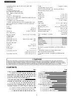
Amplifier Section

RMS Output power : Dolby Digital Mode

Front Ch

65 W per channel (6

), 1 kHz,

10% THD

Surround Ch

65 W per channel (6

), 1 kHz,

10% THD

Center Ch

65 W per channel (6

), 1 kHz,

10% THD

Subwoofer Ch

75 W per channel (4

), 100 Hz,

10% THD

Total RMS Dolby Digital mode
power

400 W

PMPO output power

3500 W

DIN Output Power : Dolby Digital Mode

Front Ch

55 W per channel (6

), 1 kHz,
1% THD

Surround Ch

55 W per channel (6

), 1 kHz,
1% THD

Center Ch

55 W per channel (6

), 1 kHz,
1% THD

Subwoofer Ch

65 W per channel (4

), 100 Hz,

1% THD

Total DIN Dolby Digital mode
power

340 W

n

FM/AM Tuner, Terminals Section

Preset station

FM 15 stations

AM/MW 15 stations

©

2005 Matsushita Electric Industrial Co. Ltd.. All

rights

reserved.

Unauthorized

copying

and

distribution is a violation of law.

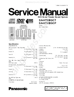
SA-HT330GCT
SA-HT330GCP

Colour
(S)... Silver Type

Frequency Modulation (FM)

Frequency range

87.50 - 108.00 MHz (50-kHz step)

Sensitivity

2.5 µV (IHF)

S/N 26 dB

2.2 µV

Antenna terminals

75

(unbalance)

Amplitude Modulation (AM/MW)

Frequency range

522 - 1629 kHz (9 - kHz step)

520 - 1630 kHz (10 - kHz step)

AM Sensitivity S/N 20 dB at 999
kHz

560 µV/m

Phone jack

Terminal

Stereo, 3.5 mm jack

Mic jack

Sensitivity

0.7mV, 1.2k

Terminal

Mono, 6.3mm (1 system)

n

Disc Section

Discs played ( 8 cm or 12 cm)

(1) DVD-RAM (DVD-VR compatible, JPEG formatted discs)

(2) DVD-Audio

(3) DVD-Video

(4) DVD-R, DVD-RW (DVD-Video compatible)
+R, +RW (video compatible)

(5) CD-Audio (CD-DA)

(6) Video CD

(7) SVCD (Conforming to IEC62107)

DVD Home Theater Sound System

Specification

ORDER NO. MD0507281C3

All manuals and user guides at all-guides.com

all-guides.com

Summary of Contents for SA-HT330GCT

Page 1: ... Ltd All rights reserved Unauthorized copying and distribution is a violation of law SA HT330GCT SA HT330GCP Colour S Silver Type Frequency Modulation FM Frequency range 87 50 108 00 MHz 50 kHz step Sensitivity 2 5 µV IHF S N 26 dB 2 2 µV Antenna terminals 75 Ω unbalance Amplitude Modulation AM MW Frequency range 522 1629 kHz 9 kHz step 520 1630 kHz 10 kHz step AM Sensitivity S N 20 dB at 999 kHz ...

Page 2: ...autions for Optical Pickup Unit 8 7 1 Cautions to be taken in handling the Optical Pickup Unit 8 7 2 Cautions to be taken when replacing the Optical Pickup Unit 8 Terminal S terminal 1 system Component video output For GCT NTSC 525 480 p 525 480 i PAL 625 576 p 625 576 i Component video output For GCP 480p 480i Y output level 1 Vp p 75 Ω PB output level 0 7 Vp p 75 Ω PR output level 0 7 Vp p 75 Ω ...

Page 3: ...rtant points in adjustment 44 17 3 Storing and handling Test Discs 44 17 4 Optical adjustment 45 18 Abbreviations 47 19 Voltage Measurement and Waveform Chart 49 19 1 Voltage Measurement 49 19 2 Waveform Chart 54 20 Block Diagram 55 20 1 DVD MODULE BLOCK 55 20 2 MAIN BLOCK 58 21 Notes of Schematic Diagram 64 22 Schematic Diagram 65 22 1 OPTICAL PICKUP UNIT CIRCUIT 65 22 2 DVD MODULE CIRCUIT 66 22 ...

Page 4: ...the chassis the reading must be Fig 1 1 1 2 LEAKAGE CURRENT HOT CHECK See Figure 1 1 Plug the AC cord directly into the AC outlet Do not use an isolation transformer for this check 2 Connect a 1 5kΩ 10 watts resistor in parallel with a 0 15µF capacitors between each exposed metallic part on the set and a good earth ground such as a water pipe as shown in Figure 1 3 Use an AC voltmeter with 1000 oh...

Page 5: ...following conditions are noticed No sound is heard when the power is turned on Sound stops during a performance The function of this circuitry is to prevent circuitry damage if for example the positive and negative speaker connection wires are shorted or if speaker systems with an impedance less than the indicated rated impedance of the amplifier are used If this occurs follow the procedure outlin...

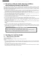
Page 6: ...cement ES device from its protective package until immediately before you are ready to install it Most replacement ES devices are packaged with leads electrically shorted together by conductive foam aluminium foil or comparable conductive material 7 Immediately before removing the protective material from the leads of a replacement ES device touch the protective material to the chassis or circuit ...

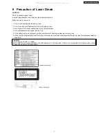
Page 7: ...lens 4 Do not disassemble the optical pick up unit 5 If the optical pick up is replaced use the manufacturer s specified replacement pick up only 6 Use of control or adjustments or performance of procedures other than those specified herein may result in hazardous radiation exposure CAUTION THIS PRODUCT UTILIZES A LASER USE OF CONTROLS OR ADJUSTMENTS OR PERFORMANCE OF PROCEDURES OTHER THAN THOSE S...

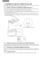
Page 8: ...when handling the flexible cable 4 The antistatic FPC is connected to the new optical pickup unit After replacing the optical pickup unit and connecting the flexible cable cut off the antistatic FPC 7 2 Cautions to be taken when replacing the Optical Pickup Unit The flexible cable of the optical pickup unit which was supplied as a component is equipped with a short clip to prevent the laser diode ...

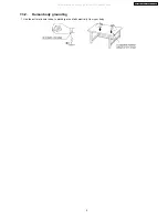
Page 9: ...7 3 2 Human body grounding 1 Use the anti static wrist strap to discharge the static electricity from your body 9 SA HT330GCT SA HT330GCP All manuals and user guides at all guides com ...

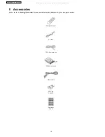
Page 10: ...Materials Accessories Parts List Section 27 4 for the part number Remote Control AC cord FM indoor antenna AM loop antenna Video cable AC Plug Adaptor Speaker Label 10 SA HT330GCT SA HT330GCP All manuals and user guides at all guides com ...

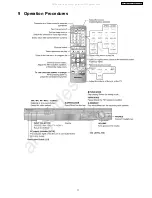
Page 11: ...9 Operation Procedures 11 SA HT330GCT SA HT330GCP All manuals and user guides at all guides com a l l g u i d e s c o m ...

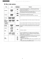
Page 12: ...10 Disc information 12 SA HT330GCT SA HT330GCP All manuals and user guides at all guides com ...

Page 13: ...13 SA HT330GCT SA HT330GCP All manuals and user guides at all guides com ...

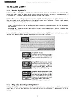
Page 14: ... video on their PC to Create a HighMAT CD or DVD which can be easily played back on consumer electronics devices such as CD and DVD players and car stereos Move digital media files using recordable media such as CD R and CD RW between the PC and various playback devices such as CD and DVD players A new standard for creating personal media on consumer electronic devices HighMAT enable easier and mo...

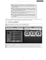
Page 15: ...T Conventional HighMAT Even though DVD player is CD R RW compatible the inconsistent ways that various DVD players can read the music or photos files often leads to a confusing and inconsistent playback experince HighMAT compatible products play content back with consistent interface This includes products which are JPEG compatible products without HighMAT support 15 SA HT330GCT SA HT330GCP All ma...

Page 16: ...16 SA HT330GCT SA HT330GCP All manuals and user guides at all guides com a l l g u i d e s c o m ...

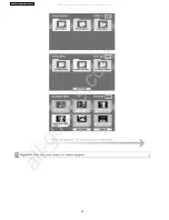
Page 17: ...t supports HighMAT you get better easier navigation You get folders you can access with a single click of your DVD player s remote control You can view important information about your music like full song names artist titles album names and genre And you can get faster startup on your home entertainment device To enjoy the benefits of HighMAT all you need is software that supports HighMAT for CD ...

Page 18: ...bly of Top Cabinet Disassembly of SMPS Module P C B Disassembly of Rear Panel Disassembly of AC Inlet P C B Disassembly of Digital Amplifier P C B Disassembly of DVD Lid when taking out disc manually Disassembly of Front Panel Disassembly of Headphone Panel and Tact Switch P C B Disassembly of DVD Mechanism unit Disassembly of Main P C B Warning This product uses a laser diode Refer to Precaution ...

Page 19: ...12 2 P C B Locations 19 SA HT330GCT SA HT330GCP All manuals and user guides at all guides com ...

Page 20: ...e P C B Follow the Step 1 Step 3 of item 12 3 Step 1 Remove 4 screws Step 2 Detach connector CN1 CN2 CN3 and remove SMPS Module P C B Note SMPS Module should be replaced as an assembly unit in case it is faulty 12 5 Disassembly of Rear Panel Follow the Step 1 Step 3 of item 12 3 20 SA HT330GCT SA HT330GCP All manuals and user guides at all guides com ...

Page 21: ...m 12 3 Follow the Step 1 Step 3 of item 12 5 Step 1 Detach connector CN1 Step 2 Remove AC inlet P C B as arrow shown 12 7 Disassembly of Digital Amplifier P C B Follow the Step 1 Step 3 of item 12 3 Follow the Step 1 Step 3 of item 12 5 Step 1 Remove 2 screws Step 2 Detach connector CN2 CN2001 and FFC CN2002 Step 3 Flip over the Digital Amplifier P C B Side A 21 SA HT330GCT SA HT330GCP All manuals...

Page 22: ... 2 Insert the gear jig into the tray open close hole Step 3 Turn the gear jig counterclockwise to open the tray Note Do not use force to push the tray backwards as it can damage the mechanism unit Turn the gear jig clockwise to return tray 12 9 Disassembly of Front Panel Follow the Step 1 Step 3 of item 12 3 Follow the Step 1 Step 3 of item 12 8 22 SA HT330GCT SA HT330GCP All manuals and user guid...

Page 23: ...own 12 10 Disassembly of Headphone Panel and Tact Switch P C B Follow the Step 1 Step 3 of item 12 3 Follow the Step 1 Step 3 of item 12 8 Follow the Step 1 Step 5 of item 12 9 Step 1 Remove Volume Knob Step 2 Remove 2 screws and panel angle Step 3 Remove 2 screws and Mecha Support Step 4 Remove 5 screws and remove Headphone Panel and 23 SA HT330GCT SA HT330GCP All manuals and user guides at all g...

Page 24: ...01 Step 4 Remove DVD Mechanism unit as arrow shown 12 12 Disassembly of Main P C B Follow the Step 1 Step 3 of item 12 3 Follow the Step 1 Step 3 of item 12 5 Follow the Step 1 Step 3 of item 12 8 Follow the Step 1 Step 5 of item 12 9 Follow the Step 1 Step 4 of item 12 11 Step 1 Remove 3 screws Step 2 Detach FFC CN2000 connector CN2001 CN3 and remove Main P C B 24 SA HT330GCT SA HT330GCP All manu...

Page 25: ...ooves at left open Step 4 Take out the traverse Unit Step 1 While pressing the stopper to the arrow direction slide the guide tray unit to remove Disassembly of DVD Module P C B Step 5 Remove 4 screws Step 6 Detach 15P FFC Board FP8271 Step 7 Detach 20P FFC Board FP8501 12 13 Disassembly and Assembly Mechanism Unit 12 13 2 Replacement of Tray Follow the Step 1 Step 7 of item 12 13 1 Replacement of...

Page 26: ...e Arm Catch from Tray Slider and Tray Fixing the Tray Step 1 Insert Tray slightly into groove of chassis Step 2 Insert Tray into the area to avoid catching the mechanism chassis claw Step 3 Latch Drive Arm Catch onto Tray and Tray Slider Step 4 Push Tray Step 5 Check Tray and Drive Arm move smoothly 26 SA HT330GCT SA HT330GCP All manuals and user guides at all guides com a l l g u i d e s c o m ...

Page 27: ...of loading section Follow the Step 1 Step 4 of item 12 13 1 Replacement of Traverse Unit Follow the Step 1 Step 5 of item 12 13 2 Replacement of Tray 27 SA HT330GCT SA HT330GCP All manuals and user guides at all guides com ...

Page 28: ...13 4 Replacement of Optical Pickup Unit Follow the Step 1 Step 5 of item 12 13 1 Replacement of Traverse Unit Follow the Step 1 Step 5 of item 12 13 2 Replacement of Tray 28 SA HT330GCT SA HT330GCP All manuals and user guides at all guides com ...

Page 29: ...Step 2 Remove 4 pins Step 3 Remove Traverse Unit Note Insert a short pin into FFC of the optical pickup 29 SA HT330GCT SA HT330GCP All manuals and user guides at all guides com ...

Page 30: ...30 SA HT330GCT SA HT330GCP All manuals and user guides at all guides com ...

Page 31: ...Step 5 of item 12 13 1 Replacement of Traverse Unit Follow the Step 1 Step 5 of item 12 13 2 Replacement of Tray Follow the Step 1 Step 11 of item 12 13 4 Replacement of Optical Pickup Unit 31 SA HT330GCT SA HT330GCP All manuals and user guides at all guides com a l l g u i d e s c o m ...

Page 32: ...32 SA HT330GCT SA HT330GCP All manuals and user guides at all guides com ...

Page 33: ...Module P C B Disassembly of Top Cabinet Follow the Step 1 Step 3 of item 12 3 Disassembly of SMPS Module P C B Follow the Step 1 of item 12 4 Disassembly of Rear Panel Follow the Step 1 Step 2 of item 12 5 Disassembly of Digital Amplifier P C B Follow the Step 1 and Step 3 of item 12 7 33 SA HT330GCT SA HT330GCP All manuals and user guides at all guides com ...

Page 34: ...m 12 9 Disassembly of Rear Panel Follow the Step 1 Step 2 of item 12 5 Disassembly of DVD Mechanism unit Follow the Step 2 and Step 4 of item 12 11 Disassembly of Main P C B Follow the Step 1 of item 12 12 Disassembly of Headphone Panel and Tact Switch P C B Follow the Step 1 Step 4 of item 12 10 Note Reconnect all the connectors CN2005 CN2006 and checking for Main Headphone Panel Tact Switch DVD ...

Page 35: ... diagnosis and tilt adjustment Be sure to use the self diagnosis function before replacing the optical pickup when NO DISC is displayed As a guideline you should replace the optical pickup when the value of the laser drive current is more than 55 Note Press the power button to turn on the power and check the value within three minutes before the unit warms up Otherwise the result will be incorrect...

Page 36: ...ommand was sent F504 Error adjusting DSC data slice offset F505 DSC Attention error Similar disposal as F500 F506 Invalid media Disc is flipped over TOC unreadable incompatible disc media ODC related F600 Access failure to management information caused by demodulation error Operation stopped because navigation data is not accessible caused by the demodulation defect F601 Indeterminate sector ID re...

Page 37: ...m version agreement check for factory preset setting failure prevention F897 Initialize is not completed Initialize completion check for factory preset setting failure prevention F898 Disagreement of hardware and software Unsuitable combination of AV DECORDER SDRAM and FLASH ROM firmware F8A0 Message command is not appropriate Begin sending message to AV task Note An error code will be canceled if...

Page 38: ...4 4 Service mode table 2 Pressing various button combinations on the player and remote control unit can activate the service modes 38 SA HT330GCT SA HT330GCP All manuals and user guides at all guides com ...

Page 39: ...39 SA HT330GCT SA HT330GCP All manuals and user guides at all guides com ...

Page 40: ...40 SA HT330GCT SA HT330GCP All manuals and user guides at all guides com ...

Page 41: ...on is activated Note The following buttons are invalid and the player displays ___LOCKED_ while the lock function mode is entered Player INPUT SELECTOR VOLUME KNOB Remote controller unit TV VCR TUNER BAND ADVANCED DISC REVIEW PLAY SPEED QUICK REPLAY 0 9 FL DISPLAY MANUAL SKIP REPEAT TOP MENU DIRECT NAVIGATOR MENU PLAYIST SETUP FUNCTIONS RETURN MUTING 14 5 2 Cancellation The lock can be cancelled b...

Page 42: ...D CD inserted in the player press and hold down the button simultaneously for at least two seconds and press the F_SKIP button for at least two seconds in order to display T 3 Press the button If a memorized error is detected the result of self diagnosis is displayed Ex T H 0 12 See table below If several errors are detected press the button to display each 15 2 2 Re Display Press the power button...

Page 43: ... to improve the quality including operability and playability to the substandard discs processing to optimize the drive The recovery disc has also firmware version up After version up recovery processing is executed automatically Part number of the recovery disc for version up will be noticed when it is supplied Updating firmware 1 Load the recovery disc that is supplied to the player and run it 2...

Page 44: ... there is a noticeable degradation in picture quality Optical adjustments cannot be made inside the optical pickup Adjustment is generally unnecessary after replacing the traverse unit 17 2 2 Important points in electrical adjustment Follow the adjustment procedures described in this Manual 17 3 Storing and handling Test Discs Surface precision is vital for DVD test discs Be sure to store and hand...

Page 45: ... the procedure with tilt adjustment Jitter value depends on the model 1 If the jitter value changes like B the optimum point is easy to find 2 If the jitter value changes like A set the optimum point near the middle 17 4 1 3 Check after adjustment Play test disc or any other disc to make sure there is no picture degradation in the inner middle and outer peripheries and no audio skipping After adju...

Page 46: ...46 SA HT330GCT SA HT330GCP All manuals and user guides at all guides com a l l g u i d e s c o m ...

Page 47: ... SERVO CONTROLLER DATA SLICE LOOP FILTER DIGITAL VIDEO DISC INITIAL LOGO ABBREVIATIONS E EC ECR ENCSEL ETMCLK ETSCLK ERROR TORQUE CONTROL ERROR TORQUE CONTROL REFERENCE ENCODER SELECT EXTERNAL M CLOCK 81MHz 40 5MHz EXTERNAL S CLOCK 54MHz F FBAL FCLK FE FFI FEO FG FSC FSCK FOCUS BALANCE FRAME CLOCK FOCUS ERROR FOCUS ERROR AMP INVERTED INPUT FOCUS ERROR AMP OUTPUT FREQUENCY GENERATOR FREQUENCY SUB C...

Page 48: ...E Q DATA SYSTEM CLOCK T TE TIBAL TID TIN TIP TIS TPSN TPSO TPSP TRCRS TRON TRSON TRACKING ERROR BALANCE CONTROL BALANCE OUTPUT 1 BALANCE INPUT BALANCE INPUT BALANCE OUTPUT 2 OP AMP INPUT OP AMP OUTPUT OP AMP INVERTED INPUT TRACK CROSS SIGNAL TRACKING ON TRAVERSE SERVO ON INITIAL LOGO ABBREVIATIONS V VBLANK VCC VCDCONT VDD VFB VREF VSS V BLANKING COLLECTOR POWER SUPPLY VOLTAGE VIDEO CD CONTROL TRAC...

Page 49: ... 1 0 4 0 1 0 3 1 9 2 7 1 7 2 6 2 6 2 6 2 6 2 7 2 7 2 4 2 5 2 5 2 6 1 8 1 9 STANDBY 0 0 0 0 0 0 0 0 0 0 0 0 0 0 0 0 0 0 0 0 Ref No MODE 141 142 143 144 145 146 147 148 149 150 151 152 153 154 155 156 157 158 159 160 CD PLAY 1 7 1 7 0 1 1 7 1 7 3 4 0 9 0 9 0 4 3 3 2 0 1 0 1 0 2 0 0 0 4 0 8 3 4 0 3 4 STANDBY 0 0 0 0 0 0 0 0 0 0 0 0 0 0 0 0 0 0 0 0 Ref No MODE 161 162 163 164 165 166 167 168 169 170 1...

Page 50: ...0 0 0 0 0 0 0 0 0 0 0 0 0 0 0 Ref No MODE 21 22 23 24 25 26 27 28 29 30 31 32 33 34 35 36 37 38 39 40 CD PLAY 1 5 2 2 2 5 1 6 2 7 2 6 0 2 6 0 8 0 8 1 6 1 0 1 0 1 0 1 0 3 4 1 7 1 1 0 8 STANDBY 0 0 0 0 0 0 0 0 0 0 0 0 0 0 0 0 0 0 0 0 Ref No MODE 41 42 43 44 45 46 47 48 CD PLAY 0 8 1 0 1 7 1 1 1 2 0 3 4 1 6 STANDBY 0 0 0 0 0 0 0 0 IC8251 IC8111 IC8421 IC8421 IC8251 IC8601 IC8606 IC8611 IC8651 IC8651 ...

Page 51: ... 0 4 7 2 1 0 0 27 8 0 27 8 27 1 28 1 0 0 28 1 27 9 28 1 28 1 STANDBY 0 0 0 0 0 0 0 0 0 0 0 0 0 0 0 0 0 0 0 0 Ref No MODE 21 22 23 24 CD PLAY 0 0 28 1 28 1 STANDBY 0 0 0 0 Ref No MODE 1 2 3 4 5 6 7 8 9 10 11 12 13 14 CD PLAY 0 1 4 5 2 1 2 3 2 1 0 0 4 2 0 2 2 2 4 0 3 1 9 4 9 STANDBY 0 0 1 0 1 0 1 0 1 0 0 2 0 1 0 1 0 1 0 1 0 1 0 2 Ref No MODE 1 2 3 4 5 6 7 8 9 10 11 12 13 14 CD PLAY 2 3 2 4 2 3 0 2 4...

Page 52: ... 2 5 0 5 0 5 0 5 0 3 0 0 Ref No MODE 21 22 23 24 25 26 27 28 29 30 31 32 33 34 35 36 37 38 39 40 CD PLAY 0 1 5 0 0 1 0 1 0 1 0 1 5 0 4 4 4 1 2 8 0 1 0 1 0 1 0 1 0 1 0 1 0 1 5 0 5 0 4 9 STANDBY 0 5 0 0 0 0 0 5 0 0 0 0 0 0 0 0 0 0 0 0 0 7 0 Ref No MODE 41 42 43 44 45 46 47 48 49 50 51 52 53 54 55 56 57 58 59 60 CD PLAY 0 1 0 1 0 1 4 9 0 1 0 1 0 1 0 1 5 0 5 0 5 0 0 1 5 0 0 1 0 1 0 1 0 1 0 1 0 1 0 1 S...

Page 53: ... 2 0 0 0 2 0 Q2100 Q2102 Q2028 Q1005 Q2000 Q2031 Q2201 Q2701 Q2702 Q2712 Q2005 Q2026 Q2820 Q2003 Q2004 Q2806 Q2030 Q2711 Q2721 Q2722 Q2805 Q2814 Q2818 Q2813 Q2807 Q2808 Q2809 Q2810 19 1 5 SMPS MODULE P C B Ref No MODE E C B E C B E C B E C B E C B CD PLAY 2 0 2 0 0 6 0 4 0 4 21 9 4 8 21 3 0 1 0 4 8 0 1 2 8 0 4 STANDBY 1 1 1 2 1 2 0 5 1 1 0 8 0 0 0 0 5 4 0 0 3 0 0 5 Ref No MODE E C B E C B E C B CD...

Page 54: ...6 PIN 6 CD PLAY 5 76Vp p 10msec div CN2006 PIN 7 CD PLAY 5 24Vp p 10msec div H2001 PIN 2 CD PLAY 1 40Vp p 10msec div H2001 PIN 4 CD PLAY 1 41Vp p 10msec div H2001 PIN 6 CD PLAY 1 41Vp p 10msec div CN2004 PIN 3 CD PLAY 5 80Vp p 10msec div H2001 PIN 10 CD PLAY 1 39Vp p 10msec div H2001 PIN 12 CD PLAY 1 40Vp p 10msec div H2001 PIN 8 CD PLAY 1 40Vp p 10msec div H2004 PIN 7 CD PLAY 5 24Vp p 10msec div ...

Page 55: ...VD TB DVD TD DVD TC DVD FE2 DVD CD FE1 DVD CD RF VREF2 RF VREF1 PIN CD SUBSEL TRACKING COIL FOCUS COIL 124 LPC01 Q8551 SWITCH Q8552 SWITCH 126 LPC02 Q8561 SWITCH Q8562 SWITCH 139 AD0 LDCD LDDVD 81 P14 QR8571 SUPPLY CONTROL SWITCH HFM VCC OUT 130 VIN9 131 VIN5 129 VIN10 132 VIN6 SUB2 SUB1 123 LPC1 PIN DVD SW 15 1M 8 SUB1 14 SUB2 13 VREF 11 RF 9 FE1 6 FE2 7 TC 4 OPTICAL PICKUP SPINDLE MOTOR UNIT TD ...

Page 56: ...8 25 A15 EXADT0 EXADT15 18 42 43 46 51 58 64 DQ0 29 36 38 45 DQ15 EXDT0 EXDT15 23 33 36 40 XWE 11 55 NEXWE XCE 26 19 NEXCE XOE 28 20 NEXOE 12 XRESET 84 NRST IC8001 DV3 2 LSI MN2DS0009AP A16 9 16 17 48 A19 EXADR16 EXADR19 41 54 56 57 A20 10 65 P0 IC8051 C3ABPG000145 64 SDRAM IC IC8651 IC8601 C0EBA0000029 VOLTAGE DETECTOR IC8606 C0EBE0000455 RESET IC RFKWMH90B160 GCP RFKWMH90C160 GCT 16M FLASH ROM I...

Page 57: ...AC4OUT 157 DAC5OUT 182 VDIO1 183 VIDO0 2 1 181 VIDO2 2 1 5 5 8 1 DVD_MIXL R DVDFL R DVDSL R DVDCNT SUBW ZFLAG PY CB_B CR_R S_Y S_C DVD_CMD DVD_STAT DVD_CLK 4 4 A 5 QR8111 SWITCH IC8001 DV3 2 LSI MN2DS0009AP Q8335 SWITCH Q8331 SWITCH Q8341 SWITCH Q8321 SWITCH Q8325 SWITCH IC8421 C0FBBK000050 AUDIO DAC IC8691 C0JBAA000346 AND GATE LOGIC IC IC8111 C0CBCBD00018 POWER SUPPLY TO MAIN BLOCK IC8695 C0JBAA...

Page 58: ... CR_R CB_B S_C S_Y PY XOUT 13 XIN 15 X2000 28 DVD_CLK DVD_CLK 29 DVD_STAT DVD_STAT 30 DVD_CMD DVD_CMD 43 DVD_MUTE ZFLAG Q2028 INVERTER SWTCH ZFLAG VIDEO OUT S VIDEO TO DVD BLOCK IC2006 C9ZB00000498 VIDEO SELECTOR IC IC2018 MICROPROCESSOR C2CBHG000197 58 SA HT330GCT SA HT330GCP All manuals and user guides at all guides com ...

Page 59: ...23 OUTLS R 24 22 OUTLSN R Q2102 MUTING SWITCH Q2201 MUTING CONTROL IC2017 C0ABBB000118 DUAL OP AMP 2 6 1 7 3 4 5 25 ECS 24 ECK 23 EDA 6 41 38 FOUT4 3 TV VCR JK3000 Q2000 RESET SWITCH D2001 3 5 6 2 48 HP_MUTE RESET 12 FILTER 51 49 VINFL R 3 5 52 50 GOUTFL R Q2703 MUTING SWITCH Q2704 53 MIC_MUTE Q6071 Q6072 Q6073 MIC AMP IC2011 C1BB00000845 ASP IC TUNER PACK J3CCBC000004 IC2019 C3EBEG000072 EEPROM I...

Page 60: ... IC2400 C1BA00000455 FRONT CHANNEL IC 71 MUTE_DAMP Q2702 SWITCH Q2701 SWITCH Q2722 SWITCH Q2721 SWITCH Q2712 SWITCH Q2711 SWITCH 70 MUTE_SUB_C 6 6 6 69 MUTE_F 68 MUTE_SUR 5 8 8 5 8 5 16 21 16 21 16 21 7 7 7 SYNC 54 MIC_SW JK6002 HEADPHONE IC2018 MICROPROCESSOR C2CBHG000197 JK6010 MIC 60 SA HT330GCT SA HT330GCP All manuals and user guides at all guides com ...

Page 61: ...0 Q2900 Q2901 11 4 X2901 2 6 34 HOP_DA 20 BEAT_PROOF 40 PCONT 9 1 8 7 3 DIN 7 CLK 8 STB 9 SWITCH SWITCH VR6000 JOG VOL 76 JOG_A 75 JOG_B FL6000 FL DISPLAY IC6000 C0HBB0000057 FL DRIVER IC IC2900 C0JBAB000011 CLOCK GENERATOR IC IC2018 MICROPROCESSOR C2CBHG000197 IC904 C0GAG0000022 RELFECTIVE PHOTO SENSOR G1 5 7 10 13 16 19 22 25 27 29 32 34 G9 P1 6 8 9 11 12 14 15 17 18 20 21 23 24 26 28 30 31 33 P...

Page 62: ... 9V VP 7 5V D2803 1 5 3 D 5V 3 D 5V 2 4 DC_DET Q2809 REGULATOR 1 D2851 D2853 D2812 D2831 L2807 2 1 4 D 1 2V 5 A 5V Q2805 Q2806 REGULATOR 3 1 L2803 Q2820 SWITCH Q2818 DCDET SWITCH Q2813 REGULATOR Q2807 Q2808 REGULATOR Q2814 REGULATOR Q2810 REGULATOR IC2804 C0CAAHG00020 9V REGULATOR 62 SA HT330GCT SA HT330GCP All manuals and user guides at all guides com ...

Page 63: ... SIGNAL LINE DVD VIDEO SIGNAL LINE CD DA AUDIO VIDEO SIGNAL LINE FM AM SIGNAL LINE E2000 L2802 L2805 D25 TO FL DISPLAY SYNC Q8 Q7 D24 Q3 Q62 T1 POWER TRANSFORMER T2 SUB TRANSFORMER F1 JK500 AC INLET NR1 L1 D12 D13 D3 MIC SIGNAL LINE Q2 Q63 Z1 Q1 Q61 Q60 Z2 Z5001 F1 L5001 63 SA HT330GCT SA HT330GCP All manuals and user guides at all guides com ...

Page 64: ...e tester or the measuring unit Importance safety notice Components identified by mark have special characteristics important for safety Furthermore special parts which have purposes of fire retardant resistors high quality sound capacitors low noise resistors etc are used When replacing any of components be sure to use only manufacturer s specified parts shown in the parts list Caution IC LSI and ...

Page 65: ... C5 22P C6 22P C1 0 1 C3 0 1 C2 0 1 R1 0 R4 0 R2 0 C8 0 1 R3 0 R5 0 R6 0 R7 6 8K C7 0 1 VR2 6 8K VR1 6 8K C4 0 22 L3 J0JBC0000105 T F F T HFM TA TB TD TC FE2 FE1 GND IM RF VREF2 RF PIN DVD LD CD LD GND LD DVD GND OEIC VREF1 VCC SUB2 SUB1 PIN CD SUBSEL GND IM GND VCC GND GND OUT GND GND TB TA TC TD FE1 FE2 IM RF GND VREF VCC SUB2 SUB1 SW LD CD LD DVD LDGND SCHEMATIC DIAGRAM 1 OPTICAL PICKUP UNIT CI...

Page 66: ...GEY0R00V LB8561 J0JBC0000042 LB8551 J0JBC0000042 LB8531 ERJ2GE0R00X R8533 0 R8531 1 5K C8533 0 1 C8256 0 1 C8253 0 1 R8251 6 8 RX8532 56 x 4 RX8533 56 x 2 C8531 100P C8532 220P RX8531 56 x 2 IC8251 C0GBG0000048 DRIVE IC IC8251 TO OPTICAL PICKUP UNIT CIRCUIT ON SCHEMATIC DIAGRAM 1 C8255 16V22 C8258 0 1 C8257 16V47 R8532 2 2K TRVFTMUTE C8262 0 1 C8261 0 1 R8262 15K R8261 82K R8263 82K R8264 15K CL82...

Page 67: ...K R8558 47K R8557 51 R8556 56 C8553 6 3V47P R8555 2 2 R8553 1K R8552 1K R8551 0 R8554 68 C8552 16V10P R8567 51 R8568 47K R8566 56 C8563 6 3V47P R8565 2 2 R8563 1K C8564 1 C8562 16V10P R8564 22 R8562 1K R8561 0 C8550 6 3V33P C8554 1 QR8571 UNR511V00L SUPPLY CONTROL SWITCH Q8562 B1ADGB000008 SWITCH Q8552 B1ADGB000008 SWITCH Q8561 2SD1819A0L SWITCH Q8551 2SD1819A0L SWITCH IC8111 C0CBCBD00018 3 3 REGU...

Page 68: ...PU_CMD CPU_STAT Y PY G CB PB B CR PR R Y C D 1 2V C8695 0 1 C8691 0 1 LB8690 J0JBC0000044 IC8421 IC8691 C0JBAA000346 AND GATE LOGIC IC IC8421 C0FBBK000050 8 CH DAC IC QR8420 UNR521100L AUDIO MUTING SWITCH IC8695 C0JBAA000346 AND GATE LOGIC IC K8106 MAIN SIGNAL LINE M 9V ZERO2 VOUT1 VOUT2 VCOM AGND2 VCC2 VOUT3 VOUT4 VOUT5 VOUT6 AGND1 VCC1 VOUT7 VOUT8 ZERO1 MS MC MD SCK DATA1 BCK LRCK VDD DGND DATA2...

Page 69: ... EXDT1 EXDT9 EXDT2 EXDT10 EXDT3 EXDT11 EXDT4 EXDT12 EXDT5 EXDT13 EXDT6 EXDT14 EXDT7 EXDT15 CL8652 NEXCE NEXOE A 5V R8333 33 Y PY G R8332 0 R8331 100 R8334 1K C8331 0 1 L8330 G1C100K00019 Y PY G_A C8330 6 3V47P IC8651 R8336 33 CB PB B R8335 100 R8337 1K C8335 0 1 CB PB B_A R8342 33 CR PR R R8341 100 R8343 1K C8341 0 1 CR PR R_A R8323 33 Y R8322 0 R8321 100 R8324 1K C8321 0 1 Y_A R8327 33 C R8326 0 ...

Page 70: ...0 1 IC8606 C0EBE0000455 RESET IC IC8601 C0EBA0000029 RESET IC C8020 0 1 C8021 0 1 C8022 0 1 C8006 0 1 EXADR4 EXADR5 EXADR6 EXADR7 EXADR17 EXADR18 EXADR19 EXADR8 EXADR9 EXADR10 EXADR11 EXADR12 EXADR13 EXADR14 EXADR15 EXADR16 EXDT15 EXDT7 EXDT14 EXDT5 EXDT12 EXDT4 EXDT6 EXDT13 EXDT11 EXDT3 EXDT10 EXDT2 EXDT9 EXDT1 EXDT8 EXDT0 NEXOE NEXCE EXADR0 CL8058 CL8059 CL8057 CL8060 CL8056 CL8061 CL8055 CL8062...

Page 71: ...0 MA11 NCSM NRAS NCAS VSS MCKI VDD33 MCK VSS NWE DQM1 DQM0 VDD12 MDQ7 MDQ8 VSS VDD33 MDQ6 MDQ9 MDQ5 MDQ10 MDQ4 MDQ11 MDQ3 MDQ12 VSS VDD33 MDQ2 MDQ13 MDQ1 MDQ14 MDQ0 MDQ15 VDD33 VSS TRCST TRCDATA3 TRC DATA2 IC8001 MN2DS0009AP DV3 2 IC C8012 0 1 C8016 0 1 C8017 0 1 C8004 0 1 C8003 0 1 CL8021 CL8022 CL8023 CL8024 CL8025 CL8026 CL8027 CL8028 CL8029 CL8030 R8003 47K C8024 0 1 CL8017 CL8016 CL8015 CL801...

Page 72: ...2 1 LB8401 J0JBC000042 C8401 15P R8621 1M R8622 1K C8622 12P C8621 12P X8621 H0J270500085 C8305 0 1 RX8401 100 x 2 R8401 100 C8025 0 1 CL8031 C8001 4V330P C8011 6 3V100P LB8001 J0JHC0000045 LB8011 J0JHC0000045 D 3 3V AD1 D 3 3V D 3 3V R8421 0 CL8213 CL8212 AMUT SBO3 STBDAC SBT3 ADOUT2 RX8403 100 x 2 ADOUT0 ADOUT1 RX8402 100 x 2 CPU_CLK CPU_CMD CPU_STAT TRCDATA1 TRCDATA0 TRCCLK SCLOCK SDATA EXTRGO ...

Page 73: ...ROUT GND2 CRIN R2890 75 C2042 6 3V1000 R2886 75 R2887 75 R2888 75 C2047 6 3V330 C2046 6 3V330 C2044 6 3V1000 C2028 1 C2029 1 C2037 0 01 C2038 10V220 C2035 0 01 S_Y C2032 0 1 C2034 0 1 C2036 50V22 C2864 16V100 C2090 0 01 W2250 0 MGND MGND DGND DGND AGND AGND DGND DGND DGND DGND ZFLAG AUDIODIGITAL ADACGND ADACGND ADACGND ADACGND ADACGND ADACGND VGND VGND VGND VGND VGND STATUS DVD_STAT CMD DVD_CMD DS...

Page 74: ...1 AOUT2 GND INFLB INFRB INCB INLSB INRSB OUTSB GND GOUTC VINC GOUTLS VINLS GOUTSUB GOUTRS VINRS VINSUB GND OUTSUBN IC2011 C1BB00000845 ASP IC R2144 1 2K A 5V B SIGNAL LINE B SIGNAL LINE MAIN SIGNAL LINE FM AM SIGNAL LINE DVD VIDEO SIGNAL LINE C2801 100P R2878 1 R2879 1 R2880 1 R2881 1 R2882 1 R2883 1 C2803 100P C2060 1 C2061 220P R2135 10K R2134 10K R2229 10K R2130 10K L2025 J0JBC0000015 L2026 J0J...

Page 75: ...P R2152 2 7K R2252 2 7K R2267 56K C2267 50V4 7 R2268 27K R2266 1 8K C2254 0 01 C2831 50V47 IC2013 C0AABB000125 DUAL OP AMP C2613 0 01 R2615 100K R2614 1K C2611 50V4 7 R2613 3 3K C2610 50V10 C2506 0 01 C2615 5600P R2617 27K R2616 68K C2612 50V4 7 C2616 16V10 R2618 1K C2505 50V1 R2505 1K Q2102 B1GFGCAA0001 MUTING SWITCH R2172 2 2K R2171 3 9K C2268 4 7 C2258 330P C2510 6800P R2251 100K C2259 330P R22...

Page 76: ...1GBCFJN0033 SWITCH R2701 2 7K UP_SW_C SW5V Q2712 B1GBCFJN0033 SWITCH R2725 1K C2725 16V10 Q2711 B1GBCFJN0033 SWITCH R2711 2 7K UP_FR Q2722 B1GBCFJN0033 SWITCH R2726 1K C2726 16V10 Q2721 B1GBCFJN0033 SWITCH R2721 2 7K UP_SUR R2700 2 2K R2703 4 7K MODE_FR MODE_SUR R2710 2 2K R2713 4 7K R2720 2 2K R2723 4 7K W2054 0 W2053 0 VREF _3 W2078 0 W2115 0 W2113 0 8 7 2 1 6 3 5 4 76 SA HT330GCT SA HT330GCP Al...

Page 77: ...009 6 3V100 R2076 100K D2000 D2002 B0ACCE000003 X2000 H2B100500004 R2097 10K C2000 0 1 R2049 220 R2047 220 R2051 220 R2052 220 R2053 220 R2054 220 D2000 D2001 D2002 R2083 680 C2006 50V2 2 C2005 10V1000 C2004 0 01 R2082 47K C2007 0 1 D2003 B0ACCK000005 L2000 G0C3R3JA0027 Q2000 B1GBCFLL0037 RESET SWITCH SYS6V VCC UP_SUR STANDBY DVD_PCONT JOG_B JOG_A STBY_LED TUN_SD HP_MUTE DVD_MUTE PCONT DC_DET TUN_...

Page 78: ...05 R2827 470 Q2805 B1ABCF000176 REGULATOR R2856 82K R2821 1 8K D2831 D2809 D2810 D2811 D2809 D2811 D2831 D2865 D2868 B0EAKM000117 C2823 1 R2898 330 R2829 1K R2826 820 C2825 6 3V330 D 1 2V A 5V R2810 1K C2824 1 C2869 1 L2802 G0A200D00002 L2003 J0JHC0000045 D2868 D2867 D2866 D2865 Q2806 B1BCCD000019 REGULATOR C2845 6 3V47 C2806 6 3V820 L2801 G0ZZ00001930 C2868 0 1 IC2804 C0CAAHG00020 9V REGULATOR IC...

Page 79: ...852 390 W2080 0 W2227 0 IC2017 C0ABBB000118 DUAL OP AMP R2120 47K GCT 10K GCP VINFL R2119 12K GCT IC2017 R2118 56K GCT GOUTFL C2123 50V10 7 5V R2117 12K GCT 10K GCP R2218 56K GCT 10K GCP GOUTFR C2125 0 01 R2219 47K GCT 10K GCP R2220 12K GCT 10K GCP C2223 50V10 VINFR 7 5V C2124 0 01 R2712 100K R2716 1K C2704 50V1 GCT 16V10 GCP Q2703 B1ABEB000002 MUTING SWITCH R2715 2 2K R2714 56K R2709 27K C2702 16...

Page 80: ...O DIGITAL AMPLIFIER CIRCUIT CN2002 ON SCHEMATIC DIAGRAM 20 H2001 W2001 TO DIGITAL AMPLIFIER CIRCUIT CN2001 ON SCHEMATIC DIAGRAM 20 JK2000 GND GND GND GND GND GND GND GND GND GND SUBWOOFER SUBWOOFER CENTER CENTER FRONT_R FRONT_R FRONT_L FRONT_L SURR_R SURR_R SURR_L SURR_L GND GND W2052 0 SPEAKERS R2937 47 R2938 47 VR6001 EVUE27FK3B53 MIC VOL 3 2 1 MIC SIGNAL LINE R6095 68 C6094 10V100 GCT C6086 100...

Page 81: ...2 G1 G3 P3 VP P4 P5 P6 P7 P8 P9 P10 P18 P16 P15 P14 P13 P12 FL R6030 82K C6017 100P FLD_STB C6009 0 01 G9 P1 P2 P3 P4 P5 G7 P6 P7 G6 P8 P9 G5 P10 G4 P13 P16 P18 G1 G9 P2 G8 P11 P12 G3 P14 P15 G2 P17 C6023 100P P1 P11 SW5V SW5V RMT RMT RMT VREF KEY1 STBY_LED H6008 W6009 VCC IC6000 C0HBB0000057 FL DRIVER IC VP G9 G8 G7 G6 G5 G4 G3 G2 G1 P4 P5 P6 P7 P8 P9 P10 P2 P3 P12 P13 P14 P15 P16 P17 P18 P19 VCC...

Page 82: ...IAGRAM 20 TO MAIN CIRCUIT H2004 W2004 ON SCHEMATIC DIAGRAM 14 R20 R22 Q3 D21 C16 C18 28V 28V GND GND 28V 28V 28V 28V C20 D15 R17 R23 R19 PC1 R18 R24 Q62 R31 R47 R63 R64 T1 D23 C17 C19 36V R53 D25 C28 13V D18 C27 C23 GND1 GND1 GND1 PCONT SYNC SYS6V FL1 FL2 R56 D50 C50 Q63 R65 D63 C61 T2 D24 C25 Q7 R37 PC3 Q8 R32 PC4 C24 PC2 R38 R40 R41 R39 C30 Z6 R42 R3 R4 D3 D64 D65 D12 R14 C12 R5 D4 Q1 R6 D5 C10 ...

Page 83: ...R1 R1 R2 F1 250V 3 15A CN1 PC4 R34 R36 C5 D1 R8 PC1 CX1 D9 C8 D10 R11 R46 C11 R9 R13 R12 Q61 R61 R62 D61 JW39 D60 Q60 R60 C60 C5002 0 22 C5001 0 22 R5001 1M F1 250V 5A GCT 250V 3 15A GCP Z5001 ERZV10D471C2 L5001 ELF18D609F FC5001 FC5002 TO DIGITAL AMPLIFIER CIRCUIT CN2004 ON SCHEMATIC DIAGRAM 20 CN2003 83 SA HT330GCT SA HT330GCP All manuals and user guides at all guides com ...

Page 84: ...ODE_SUR SW5V SW_5V HOP_DA HOP_DA DC_DET DC_DET CN2001 TO MAIN CIRCUIT H2001 W2001 ON SCHEMATIC DIAGRAM 16 C2533 0 01 C2534 0 01 C2433 0 01 C2434 0 01 C2633 0 01 C2634 0 01 SL SR FL FR C SW 27V_VSS 27V_VDD Q2801 Q2800 R2803 47K R2802 47K R2801 47K R2800 47K R2805 47K R2804 47K R2806 10K D2802 B0ACCK000005 D2801 B0ACCK000005 C2801 10 R2810 15K C2800 10 DC_DET 27V_VSS D2800 B0ACCK000005 R2809 10K 27V...

Page 85: ...6K CENTER C2628 1000P IC2600 C1BA00000455 SUBWOOFER IC 27V_VDD 27V_VSS IC2900 IC2901 C2904 470P R2903 100K R2901 1K R2902 10K HOP_DA C2903 1000P R2907 1M R2906 6 8K X2900 H2A6023A0011 Q2901 B1ADCE000012 SWITCH Q2900 X2901 H2A7003A0011 C2905 100P C2901 100P C2900 100P R2900 100K R2904 100K C2906 10 C2908 10 SW_5V R2715 22 C2715 0 1 CONN R2908 22 C2907 100P IC2901 C0JBAF000654 CLOCK GENERATOR IC IC2...

Page 86: ...2523 0 1 C2522 0 1 C2500 0 1 C2501 0 1 C2515 220P C2520 0 015 C2521 0 015 C2516 0 22 C2509 0 1 C2510 0 1 R2503 10 C2517 0 1 C2518 0 1 C2519 0 1 C2508 0 1 C2530 100V22 R2505 10 C2505 220P C2512 220P SR L2500 G0A220ZA0050 R2502 22 C2513 0 1 C2504 0 68 SL L2501 G0A220ZA0050 R2501 22 C2514 0 1 C2506 0 68 C2507 220P C2511 220P R2500 10 R2504 10 R2509 5 6K R2508 5 6K C2710 1000P R2507 5 6K C2529 1000P R...

Page 87: ...IAGRAM 16 H6005 W6005 S6003 PLAY R6024 1 2K R6023 1K R6022 1K R6029 22K S6002 PAUSE S6001 STOP S6000 OPEN CLOSE JK6002 HEADPHONE C6022 100P R6028 22K C6021 100P L6002 J0JBC0000019 L6001 J0JBC0000019 L6000 J0JBC0000019 C6001 0 047 C6000 0 047 C6002 1000P R6099 1 8K CD TRAY LOADING CIRCUIT CS901 S901 PLAY S902 OPEN C984 25V10 RM902 VCC OUT2 NC GND VS OUT1 VREF IC904 C0GAG0000002 REFLECTIVE PHOTO SEN...

Page 88: ...8232 R8232 R8231 C8008 C8602 C8606 IC8601 IC8606 C8601 R8601 R8003 C8023 RX8611 R8611 C8529 R8211 D8211 C8541 R8541 C8226 C8225 R8225 C8222 C8221 R8221 C8304 C8305 LB8401 RX8401 C8022 C8021 C8007 C8006 C8020 RX8403 R8401 RX8402 C8017 C8019 C8018 IC8001 C8005 C8313 R8314 R8313 C8312 C8015 IC8421 LB8301 LB8302 LB8303 LB8304 LB8305 LB8561 LB8551 LB8571 C8401 RX8031 R8041 RX8691 RX8001 C8016 RX8016 RX...

Page 89: ... C8695 C8691 IC8695 IC8691 QR8111 RX8111 L8330 C8330 C8252 L8302 L8301 C8301 C8201 C8302 C8501 L8501 L8201 R8002 C8514 C8513 C8515 C8516 C8203 C8621 C8311 R8311 R8312 C8306 R8621 R8622 C8026 C8622 C8025 C8652 C8651 C8303 LB8001 LB8011 C8251 IC8651 LB8690 IC8611 C8001 C8611 C8011 C8202 C8057 C8056 C8052 C8051 C8053 C8054 IC8051 C8055 R8013 RX8020 X8621 SIDE B CL8007 X CL8032 X CL8006 X CL8009 CL803...

Page 90: ...5 R2251 R2152 R2252 R2267 R2253 R2151 C2154 R2077 W2083 W2056 W2055 C2259 C2243 C2242 W2078 R2505 R2618 W2046 W2077 R2803 R2804 Q2030 C2510 R2503 R2613 R2405 R2305 C2504 C2503 W2012 R2504 R2506 C2613 R2614 R2615 IC2015 C2506 R2616 R2617 C2615 R2407 R2307 R2263 C2037 C2032 C2035 C2034 C2028 C2029 W2250 R2163 C2039 IC2006 W2071 W2034 L2027 L2025 L2026 L2023 L2024 L2022 C2805 C2807 R2891 R2890 C2803 ...

Page 91: ... R2048 R2049 R2047 R2062 R2061 R2064 R2060 C2001 R2072 R2071 R2065 R2080 R2069 R2067 R2068 W2121 R2897 R2046 R2056 R2057 D2001 D2000 D2002 R2083 C2004 W2120 R2037 R2036 R2038 R2034 R2032 R2035 R2018 R2030 R2033 R2031 R2025 R2027 R2026 R2000 R2001 R2002 R2003 R2077 R2076 R2028 R2016 R2029 R2006 R2017 D2003 Q2000 R2019 R2007 W2118 C2008 C2007 R2082 R2094 R2093 C2021 C2020 C2019 R2092 C2022 W2115 R20...

Page 92: ...7 H6008 W6009 W6102 W6109 W6108 W6110 FL6000 VOLUME PHONES R6038 R6005 R6006 R6007 H6009 W6009 W6053 W6054 W6055 R6022 R6024 C6022 C6021 R6029 L6002 C6000 R6099 L6001 C6001 C6002 R6028 R6023 L6000 R6009 W6010 R6050 R6051 R6012 R6030 C6023 C6016 R6019 C6017 R6017 L6003 D6008 C6012 R6011 W6051 D6006 R6013 W6040 W6044 W6009 W6030 W6031 W6025 W6020 W6024 W6021 W6027 W6035 W6034 W6032 W6029 W6028 W6026...

Page 93: ...2600 C2630 C2610 C2620 C2609 C2509 C2520 C2510 C2502 C2503 C2500 C2501 C2521 C2519 C2516 C2518 C2418 C2416 C2419 C2421 C2401 C2400 C2403 C2402 IC2400 C2410 C2420 C2409 C2705 C2706 C2707 C2530 C2430 C2504 C2406 C2404 C2606 C2604 R2502 R2501 R2401 R2402 R2601 R2602 L2700 C2515 R2504 R2503 R2404 C2415 R2403 C2615 R2603 C2608 C2617 C2417 C2408 C2508 C2517 C2514 C2513 C2414 C2413 C2614 C2613 C2715 R260...

Page 94: ...0F GCT REPX0490G GCP H PbF PbF 2 1 4 3 JK5000 CN2003 W2 W1 W421 W422 W423 W424 110V 127V 220V 230V 240V 50 60HZ AC IN S902 OPEN SW S901 PLAY SW IC904 C984 CS901 M C5001 C5002 FC5002 FC5001 R5001 Z5001 L5001 F1 250V T5AH 5 4 3 2 1 1 2 3 4 5 6 7 8 9 7 6 5 4 3 2 1 94 SA HT330GCT SA HT330GCP All manuals and user guides at all guides com ...

Page 95: ...BWOOFER SPEAKERS S VIDEO COMPONENT VIDEO OUT TV AUDIO OUT VCR AUDIO OUT JK2000 H2004 W2004 1 12 H2001 W2001 12 1 CN2000 15 1 16 2 JK3000 CN2002 10 1 H2000 W2000 1 7 CN2004 50 2 48 4 49 1 47 3 CN2006 14 2 13 1 CN2005 1 8 SOLDER SIDE PHONES VOLUME SOLDER SIDE VR6001 MIC VOLUME JK6010 MIC PbF PbF PbF PbF MAIN P C B HEADPHONE P C B OPTICAL PICKUP UNIT TO SPINDLE MOTOR 95 SA HT330GCT SA HT330GCP All ma...

Page 96: ... 1 CN1 CN2 6 1 CN3 12 1 BLACK WHITE SMPS MODULE P C B DIGITAL AMPLIFIER P C B SOLDER SIDE AC IN 110V 127V 220V 230V 240V 50 60HZ SOLDER SIDE SENSOR SOLDER SIDE SOLDER SIDE SOLDER SIDE PbF PbF PbF PbF PbF M PANEL P C B CD TRAY LOADING P C B AC INLET P C B 96 SA HT330GCT SA HT330GCP All manuals and user guides at all guides com a l l g u i d e s c o m ...

Page 97: ...0GBG0000048 28p C0GAG0000022 9p C0DAAMH00010 C0CAAHG00020 1 2 3 RFKWMH90B160 RFKWMH90C160 B1ACKD000005 B1GFGCAA0001 2SD1819A0L UNR521100L B1ADCF000001 UNR511V00L B1GDCFGA0018 2SB1218ARL B1ABCF000176 B1ADCE000012 2SD0601AHL B1ADGB000008 B1GBCFJA0028 B1AAKD000014 B1GBCFLL0037 B1GBCFJN0033 B1ABEB000002 B1ABCF000011 B1BCCG000023 B1BCCD000019 B1BACD000018 XP0621400L 2SD21370PA B0ACCE000003 MA2J11100L B...

Page 98: ...RGB_H O Mute signal 1 for video output 46 ASP_CLK O Clock signal for 6ch VOL ASP 47 ASP_DAT O Data signal for 6ch VOL ASP 48 HP_MUTE O Head Phone Mute signal 49 TUN_SD O Station Detect 50 TUN_CLK O Clock for Tuner 51 TUN_DO O Stereo Detect 52 SCART_ MUTE O Line out for SCART terminal 53 MIC_MUTE O Muting circuit for the MIC input Pin No Terminal Name I O Function 54 MIC_SW MIC Insertion Detect if ...

Page 99: ...e values are in ohms unless specified otherwise 1K 1 000 OHM The marking RTL indicates that the Retention Time is limited for this items After the discontinuation of this assembly in production the item will continue to be available for a specific period of time The retention period of a availability is dependent on the type of assembly and in accordance with the laws governing part and product re...

Page 100: ...27 1 DVD Loading Mechanisms 27 1 1 DVD Loading Mechanism Parts Location 100 SA HT330GCT SA HT330GCP All manuals and user guides at all guides com ...

Page 101: ...LEVER M 324 RML0631 TRAY SLIDER M 325 RMM0247 2 DRIVE RACK M 326 RMM0248 SUB RACK M 327 RMC0387 SUPPORT SPRING M 329 RMR1446 X CLAMPER M 330 XTN26 6GFJ SCREW M 331 XTV2 6GFJ SCREWS M 333 XWG6FFY WASHER M 334 RMR1447 X MAGNET HOLDER M 335 RMR1468 K CLAMP PLATE M 401 RAE2012Z S DU69U TRAVERSE UNIT M 402 RMG0598 A FLOATING RUBBER M 403 RMG0617 H CUSHION RUBBER A M 404 RMG0618 H CUSHION RUBBER B M 405...

Page 102: ...27 2 Cabinet Part List 27 2 1 Cabinet Parts Location 102 SA HT330GCT SA HT330GCP All manuals and user guides at all guides com ...

Page 103: ...103 SA HT330GCT SA HT330GCP All manuals and user guides at all guides com ...

Page 104: ... PANEL M GCP 14 RGWX0076 S VOLUME KNOB M 15 RHD26046 SCREW M 16 RHD30007 1SJ SCREW M 17 RHD30070 EARTH TERMINAL M 18 RHD30090 1 SCREW M 19 RHD30102 1 SCREW M 20 RHD30119 S SCREW M 21 RKMX0107 S TOP CABINET M 22 RKWX0251 Q FL WINDOW M 23 RMAX0071 MECHA SUPPORT M 24 RMCX0030 HEAT SINK CLIP M 25 RMKX0110 BOTTOM CHASSIS M 26 RMNX0156 FL HOLDER M 27 RMNX0157 POWER PCB INSULATION M 28 RGKX0314A S DVD LI...

Page 105: ...0 B1ABCF000176 TRANSISTOR M Q2801 B1ADCE000012 TRANSISTOR M Q2805 B1ABCF000176 TRANSISTOR M Q2806 B1BCCD000019 TRANSISTOR M Q2807 B1BCCG000023 TRANSISTOR M Ref No Part No Part Name Description Remarks Q2808 B1ADCF000001 TRANSISTOR M Q2809 B1ACKD000005 TRANSISTOR M Q2810 B1BACD000018 TRANSISTOR M Q2813 B1AAKD000014 TRANSISTOR M Q2814 2SD21370PA TRANSISTOR M Q2818 B1GBCFJA0028 TRANSISTOR M Q2820 B1B...

Page 106: ... CHIP CAPACITOR M L2004 G0A200D00002 COIL M L2010 G0C220JA0055 COIL M L2020 G0C220JA0055 COIL M L2022 J0JBC0000015 CHIP INDUCTOR M L2023 J0JBC0000015 CHIP INDUCTOR M Ref No Part No Part Name Description Remarks L2024 J0JBC0000015 CHIP INDUCTOR M L2025 J0JBC0000015 CHIP INDUCTOR M L2026 J0JBC0000015 CHIP INDUCTOR M L2027 J0JBC0000015 CHIP INDUCTOR M L2400 G0A220ZA0050 INDUCTOR COIL M L2401 G0A220ZA...

Page 107: ...GEY0R00V CHIP RESISTOR M W2080 ERJ6GEY0R00V CHIP RESISTOR M W2081 ERJ6GEY0R00V CHIP RESISTOR M W2082 ERJ6GEY0R00V CHIP RESISTOR M W2083 ERJ6GEY0R00V CHIP RESISTOR M W2088 ERJ3GEY0R00V CHIP JUMPER M W2091 ERJ3GEY0R00V CHIP JUMPER M W2092 ERJ3GEY0R00V CHIP JUMPER M W2093 ERJ3GEY0R00V CHIP JUMPER M W2094 ERJ3GEY0R00V CHIP JUMPER M W2095 ERJ3GEY0R00V CHIP JUMPER M W2096 ERJ3GEY0R00V CHIP JUMPER M W209...

Page 108: ...1 16W M Ref No Part No Part Name Description Remarks R2094 ERJ3GEYJ223V 22K 1 16W M R2095 ERJ3GEYJ472V 4 7K 1 16W M R2097 ERJ3GEYJ103V 10K 1 16W M R2100 ERJ3GEYJ223V 22K 1 16W M R2101 ERJ3GEYJ104V 100K 1 16W M R2111 ERJ3GEYJ333V 33K 1 16W M R2116 ERJ3GEYJ104V 100K 1 16W M R2117 ERJ3GEYJ103V 10K 1 16W M GCP R2117 ERJ3GEYJ123V 12K 1 16W M GCT R2118 ERJ3GEYJ103V 10K 1 16W M GCP R2118 ERJ3GEYJ563V 56K...

Page 109: ...2V 1K 1 16W M R2625 ERJ3GEYJ223V 22K 1 16W M Ref No Part No Part Name Description Remarks R2700 ERJ3GEYJ222V 2 2K 1 16W M R2701 ERJ3GEYJ272V 2 7K 1 16W M R2703 ERJ3GEYJ472V 4 7K 1 16W M R2708 ERJ3GEYJ182V 1 8K 1 16W M R2709 ERJ3GEYJ273V 27K 1 16W M R2710 ERJ3GEYJ222V 2 2K 1 16W M R2711 ERJ3GEYJ272V 2 7K 1 16W M R2712 ERJ3GEYJ101V 100 1 16W M R2712 ERJ3GEYJ104V 100K 1 16W M R2713 ERJ3GEYJ101V 100 1...

Page 110: ...K 1 16W M R6089 ERJ3GEYJ184V 180K 1 16W M R6090 ERJ3GEYJ102V 1K 1 16W M R6091 ERJ3GEYJ101V 100 1 16W M R6095 ERJ3GEYJ680V 68 1 16W M R6099 ERJ3GEYJ182V 1 8K 1 16W M Ref No Part No Part Name Description Remarks R8002 ERJ2GEJ473X 47K 2W M R8003 ERJ2GEJ473X 47K 2W M R8011 ERJ2GEJ220X 22 2W M R8012 ERJ2GEJ220X 22 2W M R8013 ERJ2GEJ220X 22 2W M R8041 ERJ2GEJ330X 33 2W M R8211 ERJ2GEJ103X 10K 2W M R8221...

Page 111: ...1 ECEA1HKA4R7I 4 7 50V M C2123 ECEA1HKA100I 10 50V M C2124 ECJ1VB1E103K 0 01 25V M Ref No Part No Part Name Description Remarks C2125 ECJ1VB1E103K 0 01 25V M C2138 ECJ1VC1H221J 220P 50V M C2141 ECJ1VC1H101K 100P 50V M C2149 ECJ1VB1A105K 1 10V M C2151 ECJ1VC1H101K 100P 50V M C2152 ECJ1VC1H470J 47P 50V M C2153 ECA1CM101B 100 16V M C2154 ECJ1VB1E103K 0 01 25V M C2155 ECJ1VB1H102K 1000P 50V M C2156 EC...

Page 112: ...10V M C2605 ECJ2VC2A221J 220P 100V M C2606 ECUV1C224KBV 0 22 16V M Ref No Part No Part Name Description Remarks C2606 ECQV1H684JL3 0 68 50V M C2607 ECJ1VB1H104K 0 1 50V M C2607 ECJ2VC2A221J 220P 100V M C2608 ECJ1VB1A184K 0 18 10V M C2608 ECJ3YB2A104K 0 1 100V M C2609 ECJ1VB1H822K 8200P 50V M C2609 ECJ2FB1H104K 0 1 50V M C2610 ECEA1HKA100B 10 50V M C2610 ECJ2FB1H104K 0 1 50V M C2611 ECEA1HKA4R7I 4 ...

Page 113: ...6079 ECJ1VB1H102K 1000P 50V M C6080 ECJ1VC1H101K 100P 50V M Ref No Part No Part Name Description Remarks C6082 ECEA1HKA010B 1 50V M C6086 ECJ1VB1H102K 1000P 50V M C6087 ECEA1AKA101B 100 10V M C6093 ECJ1VB1H104K 0 1 50V M C6094 ECEA1AKA101B 100 10V M GCT C8001 EEE0GA331WP 330P 4V M C8003 ECJ0EF1C104Z 0 1 16V M C8004 ECJ0EF1C104Z 0 1 16V M C8005 ECJ0EF1C104Z 0 1 16V M C8006 ECJ0EF1C104Z 0 1 16V M C8...

Page 114: ...8527 ECJ0EB1A333K 0 033 10V M C8528 ECJ1VB0J105K 1 6 3V M C8529 ECJ1VB0J105K 1 6 3V M C8530 ECJ0EF1C104Z 0 1 16V M C8531 ECJ0EC1H101J 100P 50V M C8532 ECJ0EC1H221J 220P 50V M C8533 ECJ0EF1C104Z 0 1 16V M C8541 ECJ0EB1E472K 4700P 25V M C8550 F2G0J330A031 33P 6 3V M C8551 ECJ0EF1C104Z 0 1 16V M C8552 F2G1C100A072 10P 16V M C8553 F2G0J470A031 47P 6 3V M C8554 ECJ1VB0J105K 1 6 3V M C8561 ECJ0EF1C104Z ...

Page 115: ...escription Remarks A1 1 RKK HTR0051K R C BATTERY COVER M A2 K2CQ2CA00002 AC CORD M A3 RQT8103 B O I BOOK En M GCT A3 RQT8104 G O I BOOK Cn Ar M GCT A3 RQT8227 M O I BOOK Sp M GCP A4 RSA0007 L FM ANTENNA M A5 N1DAAAA00002 AM LOOP ANTENNA M A6 K2KA2BA00001 VIDEO CABLE M A7 K2DA42E00001 AC PLUG ADAPTOR M GCP A8 RQCA0968 SPEAKER LABEL M 27 4 Packaging Materials Accessories Parts List 27 5 Packaging 11...

Reviews: