background image

Amplifier Section

THD 10%, both channels driven

HIGH

2 X 6 W (6

)

LOW

2 X 14 W (6

)

Total BI-AMP power

2 X 20 W

Input sensitivity

AUX

320 mV

P-MD

100 mV

Input impedance

AUX

22 k

P-MD

10 k

Output impedance

Headphone

16-32

FM tuner section

Frequency range

87.50-108.00 MHz

(0.05 MHz steps)

Sensitivity

1.8µV (IHF)

S/N 26 dB

1.5µV

Antenna terminals

75

unbalanced

AM tuner section

Frequency range

522-1629 kHz (9kHz steps)

Sensitivity

S/N 20 dB

500 µV/m

© 1999 Matsushita Electronics (S) Pte. Ltd. All rights
reserved. Unauthorized copying and distribution is a
violation of law.

SA-PM30MD

Colour

(S)... Silver Type

Area

(EB)... Great Britain

(EG)... Germany and Italy

TAPE SECTION

AR2 MECHANISM SERIES

CD SECTION

RAE0155Z TRAVERSE DECK SERIES

MD SECTION

MR3 MECHANISM SERIES

Cassette Deck Section

Track system

4 track, 2 channel

Heads

Record/playback

Solid permalloy head

Erasure

Double gap ferrite head

Motor

DC servo motor

Recording system

AC bias 100kHz

Erasing system

AC erase 100kHz

Tape speed

4.8 cm/s

Overall frequency reponse (±3dB at
DECK OUT)

NORMAL (TYPE I)

50- Hz - 13 kHz

HIGH (TYPE II)

50- Hz - 13 kHz

S/N ratio

Normal (TYPE I)

52dB (A weighted)

Wow and flutter

0.18 % (WRMS)

Fast forward and rewind time

Approx. 120 seconds with C-60

cassette tape

MD section

System

Minidisc digital audio system

Recording

Magnetic field modulation direct

overwrite

MD Stereo System

Specification

ORDER NO. MD9912156C2

Summary of Contents for SA-PM30MD

Page 1: ...S Silver Type Area EB Great Britain EG Germany and Italy TAPE SECTION AR2 MECHANISM SERIES CD SECTION RAE0155Z TRAVERSE DECK SERIES MD SECTION MR3 MECHANISM SERIES Cassette Deck Section Track system 4 track 2 channel Heads Record playback Solid permalloy head Erasure Double gap ferrite head Motor DC servo motor Recording system AC bias 100kHz Erasing system AC erase 100kHz Tape speed 4 8 cm s Over...

Page 2: ...mponent Replacement Procedures 9 9 Self Diagnostic Display Function 19 For EB AC 230 240 V 50Hz For EG AC 220 230 V 50Hz Power consumption 74 W Standby ECO 0 6 W NORMAL 8 5 W Dimensions WxHxD 195x288x292 mm Weight 5 6 kg Notes 1 Specifications are subject to change without notices Weight and dimensions are approximate 2 Total harmonic distortion is measured by the digital spectrum analyzer US and ...

Page 3: ... 2 Protection Circuitry The protection circuitry may have operated if either of the following conditions are noticed No sound is heard when the power is turned on Sound stops during a performance The function of this circuitry is to prevent circuitry damage if for example the positive and negative speaker connection wires are shorted or if speaker systems with an impedance less than the indicated ...

Page 4: ... The short land between the No 25 LD GND and No 24 LD pins on the flexible board is shorted with a solder builder up to prevent damage to the laser diode 3 Take care not to apply excessive stress to the flexible board FFC 4 Do not turn the variable resistor laser power adjustment It has already been adjusted Grounding for electrostatic breakdown prevention 1 Human body grounding Use the anti stati...

Page 5: ...e ACHTUNG Dieses Produkt enthält eine Laserdiode Im eingeschalteten Zustand wird unsichtbare Laserstrahlung von der Lasereinheit abgestrahlt Wellenlänge 780nm Maximale Strahlungsleistung der Lasereinheit 100W VDE Die Strahlung an der Lasereinheit ist ungefährlich wenn folgende Punkte beachtet werden 1 Die Lasereinheit nicht zerlegen da die Strahlung an der freigelegten Laserdiode gefährlich ist 2 ...

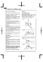
Page 6: ...6 Caution for AC Mains Lead 6 SA PM30MD ...

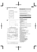
Page 7: ...7 Operation Procedures 7 SA PM30MD ...

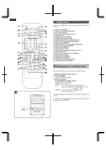
Page 8: ...8 SA PM30MD ...

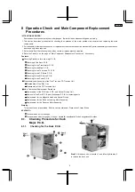
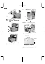
Page 9: ...cedures if necessary Contents Checking Procedure for each major P C B Checking of the Deck P C B Checking for the Transformer P C B Checking for the Main P C B Checking for the Tuner and FL P C B Checking for the CD Servo P C B Checking for the MD Servo P C B Checking for the Power P C B Diaassembly and Assembly of the Disc Tray and CD Traverse Unit Disassembly of the Disc Tray Disassembly of the ...

Page 10: ...r P C B Check the Transformer P C B as shown 8 1 3 Checking for the Main P C B Step 2 Remove the panel in the direction of arrow Check the Main P C B as shown 8 1 4 Checking for the Tuner and FL P C B Step 1 Desolder 4 points and remove the shield plate 10 SA PM30MD ...

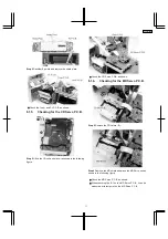
Page 11: ...s shown in the following figure Check the CD Servo P C B as shown 8 1 6 Checking for the MD Servo P C B Step 2 Remove the CD fixture B Step 4 Remove the MD shield and place the MD Servo unit as shown in the following figure Check the MD Servo P C B as shown When checking the IC1 on the MD Servo P C B it can be measured with test point on the MD Servo P C B 11 SA PM30MD ...

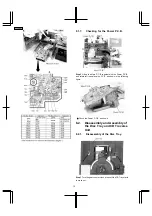
Page 12: ...B and rotate left then place the P C B as shown in the following figure Check the Power P C B as shown 8 2 Disassembly and Assembly of the Disc Tray and CD Traverse Unit 8 2 1 Disassembly of the Disc Tray Step 1 Turn the gear counter clock wise until the CD Tray starts to move out 12 SA PM30MD ...

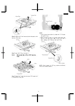
Page 13: ...move the CD Traverse Unit in the direction of the arrow NOTE 1 Follow the reverse procedure to replace the CD Traverse Unit and CD Tray 2 Make sure that the 2 gear is in position shown above and the hole on the right gear is align with the hole below it when replacing the CD Traverse Unit and CD Tray NOTE When replacing the CD Tray make sure the Dented line is at the position as shown 13 SA PM30MD...

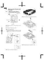
Page 14: ...B Step 3 Remove the flexible cable at CN701 Removal of the flexible cable Push the top of the connector in the direction of the arrow 1 and then pull out the flexible cable in the direction of the arrow 2 NOTE Insert a short pin into the flexible cable Step 4 Push the lever in and turn the gear clock wise fully Step 6 Release the claw and remove the Driver Plate 14 SA PM30MD ...

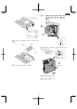
Page 15: ...g NOTE Do not touch the Lense on the OPU 8 3 2 Removal of the Deck P C B and Mechanism P C B for replacing parts Step 2 Push the lever upward to open the cassette lid and remove the deck unit Step 4 Desolder the motor wires Step 5 Remove the Deck P C B 15 SA PM30MD ...

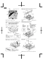
Page 16: ...FCs from the connector Step 2 Remove the pressure spring from latch Step 3 Release the 2 claws and then lift up the holder ass y Step 4 Set the holder ass y and MD mechanism unit at a 60 degree angle and then pull out the holder ass y Step 7 Spread the lugs of head shifter and then release the lugs from boss Step 9 Release the 2 claws and then remove the REF base 16 SA PM30MD ...

Page 17: ...p 15 Remove the nut plate spring and nut plate Notice for installing the optical pickup Step 2 Align the guide portion A of optical pickup with the sub shaft Note Take care not to bend the FFC 17 SA PM30MD ...

Page 18: ...with the main rack slot Step 8 Set the holder ass y and MD mechanism unit at a 60 degree angle and then pull out the holder ass y Notice for installing the loading motor Align the hole of loading motor with the boss of mechanism chassis and then install the loading motor 8 3 5 Replacement for the Traverse Motor Assembly Follow Step 1 Step 8 of item 1 3 4 in Main Component Replacement Procedures 18...

Page 19: ... displayed on FL 4 If more than 1 error exists the display will sequentially show the respective error codes each time the STOP button is pressed Notice for installing the traverse motor Align the hole of traverse motor with the boss of mechanism chassis and then install the traverse motor 9 2 Cassette Mechanism Test For error code H01 H02 H03 H06 F01 F02 1 Load a cassette tape with the erasure pr...

Page 20: ...e circuit board is disconnected Displayed when the disc is scratched too F22 MD cannot be loaded MD loading motor or MD loading mechanism error check and replace F28 MD cannot be loaded Confirm that the disc is not catching on anything The connection flexible circuit board or connector cable between the MD unit and the MD servo circuit board is disconnected or damaged check and replace if neccessa...

Page 21: ...nce in the peak level between the left and right channels does not exceed 0 5dB 4 Perform the same adjustment in reverse playback mode Check of the level difference forward and reverse directions 5 Playback the playback gain adjustment portion 315Hz 0dB of test tape QZZCFM Check if level difference between forward and reverse direction is within 1 5dB 6 After the adjustment apply screwlock to the ...

Page 22: ...ONIC VOLTMETER or OSCILLOSCOPE ADJUSTMENT Shown in Fig 3 REMARKS CONNECTIONS FREQUENCY Fashion a loop of several turns of wire and radiate a signal into the loop ant of receiver 450kHz 30 Mod at 400Hz Point of non interference on about 600kHz Headphones Jack 32Ω Fabricate the plug as shown in Fig 2 and then connect the lead wires of the plug to the measuring instrument Z102 AM IFT Adjust for maxim...

Page 23: ... especially careful with the static electricity The optical pickup is structured extremely precisely Do not subject to the strong impact or shock Do not touch the lens 2 About handling the magnetic head When replacing the magnetic head do not tighten the mounting screw RHD17022 too firmly If the screw is tightened too much to deform the resin the position of the head is moved and this affects its ...

Page 24: ...kup 5 Press MEMORY ENTER button on the unit FL display ROUGH ADJ OK flash for 3 times and display the next indication FL display FINE ADJ Write power adjustment mode 6 Adjust VR1 until reading of the laser power meter is within the standard value Fig 3 Standard value write power 6 8mW 0 1mW Cautions Do not allow the write power to reach or exceed 7 5mW even for a moment Doing so will result in dam...

Page 25: ...AP BA4558FE2 2SB1295 6 TB DTC114YETL 2SB1462STX 2SA1037AKSTX 2SC1740SRTA 2SC2787LTA RVTDTA114EST RVTDTA144EST 2SC1740SLNST RVTDTC143EST RVTDTC114EST RVTDTC114YST RVTDTC144EST 2SJ278MYTR 2SK1764KYTR 2SB1121ST TD RVTDTA143XST RVTDTA143TST RVTDTC124TST RVTDTC114TST RVTDTC143XST 2SA1309ARTA 2SB1030RTA 2SD592ARTA 2SB621ARTA 2SA952LTA 2SC1845FTA 2SD965RTA 2SC2001LTA 2SB1566E 2SJ498CTA A Ca Anode Cathode...

Page 26: ...cus coil driver output terminal 14 VO3 O Focus coil driver output terminal 15 VO2 O Traverse motor drive output terminal 16 VO2 O Traverse motor drive output terminal 17 VO1 O Spindle motor drive output terminal 18 VO O Spindle motor drive output terminal 19 PGND GND terminal 20 PVcc1 I Power supply terminal Pin No Mark I O Function 23 OFT O O Off track detection signal output terminal 24 GND GND ...

Page 27: ...gnal output 56 SCTSY O ADIP synchronous noise output terminal 57 SGSYNC O Frame synchronous signal output terminal 58 DVDD1 I Power supply terminal 59 IVDD1 Power supply terminal for I O pad Pin No Mark I O Function 60 DVss1 GND terminal 61 FS384 O 384 Fs output terminal 62 SCL O Bit clock output terminal 63 SWS O Word clock output terminal 64 SDAP O Audio data output terminal 65 SDAR I Audio data...

Page 28: ...t used open Pin No Mark I O Function 41 EEPDATA I O EEPROM data in output terminal Connected to GND through resistor 42 TEST04 O Test signal output terminal Not used open 43 TEST05 44 CFSYNC I ATRACK management frame simultaneous signal input terminal 45 TEST06 O Test signal output terminal Not used open 46 TEST07 I Connected to rec play switch signal 47 TOK OK O Not used open 48 HF ON Drive signa...

Page 29: ...l Output L Feed 12 TLOCK O Tracking Servo Feeding Signal Output L Feed Pin No Mark I O Function 14 18 A4 A8 I DRAM address 4 8 input terminal 22 OE I DRAM output enable input terminal Not used connected to GND 23 CAS I DRAM calam address strobe input terminal 24 DO3 I O DRAM data 3 in output terminal 25 DO4 I O DRAM data 4 in output terminal 26 VSS GND terminal Pin No Mark I O Function 16 CROSS O ...

Page 30: ...ut 2 PC2 I Turntable Motor Drive Signal L ON 3 IN1 I Motor Driver 1 Input 4 PC1 Traverse Motor Drive Signal L ON 5 NC No connection Pin No Mark I O Function 55 SUBC O Sub Code Serial Data Output Not Used Open 56 SBCK I Clock Input for Sub Code Serial Data 57 VSS I GND 58 X1 IN I Crystal Oscillating Circuit Input f 16 9344 MHz 59 X2 OUT O Crystal Oscillating Circuit Input f 16 9344 MHz 60 VDD I Pow...

Page 31: ... No Mark I O Function 18 D4 O Motor Driver 4 forward action output 19 PVCC2 I Power Supply 2 for Driver 20 PGND2 Ground Connection 2 for Driver 21 NC NC No Connection 22 NC NC No Connection 23 NC NC No Connection 24 NC NC No Connection 25 VCC I Power Supply Terminal 26 VREF I Reference Voltage Input 27 IN4 I Motor Driver 4 Input 28 IN3 I Motor Driver 3 Input Pin No Mark I O Function 41 MDX2REC I O...

Page 32: ...85 N C I O Open 86 N C I O Open 87 N C I O Open 88 N C I O Open 89 N C I O Open 90 LED 1 I O LED Control active L Pin No Mark I O Function 91 DES1 I O Destination Setup 1 92 DES2 I O Destination Setup 2 93 OPEN_H I O CD Tray Open Control active H 94 CLOSE_L I O CD Tray Close Control active L 95 GND D A Converter Reference GND 96 N C I O Open 97 N C I O Open 98 N C I O Open 99 N C I O Open 100 VRef...

Page 33: ... POWER DRIVE LDO APC PD LD IN APC REF TEMP IN TEMP ADIP TBAL TOFS Q2 B AS GAIN AS LNP AB GAIN TE TGAIN FE FBAL ADIP TBAL TOFS TEMP APC REF NRECT TH1 HFON1 VR1 LASER POWER ADJ B B 1 47 48 46 42 45 B CLPF1 C CENVC D A CLPF2 F2 44 43 41 40 F1 RF2 RF1 VREF MD OPTICAL PICKUP SW RF1 RF2 F1 F2 A B C D I E J F D A C B COMP COMP COMP COMP TBAL DIRECTION DET DIRECTION DET DIRECTION DET DIRECTION DET 1 2 PVC...

Page 34: ...PC GEN MICRO COMPUTER SERIAL INTERFACE ATRAC DIGITAL SIGNAL PROCESSOR ECC SPM CONTROL SELECTOR FS CONVERTER DIGITAL IN DIN PLL MASTER PLL CLOCK GEN B MONI0 3 74 77 NRST 50 MSPMDARST APCD APCREF 92 SSCK 52 SELAD SSDW SSDR 51 53 54 SELAD SSDW SSDR SSCK SGSYNC 57 SGSYNC RX1 RX2 70 71 XO 85 XI 84 AVDD0 1 IVDD0 2 DVDD0 2 16 98 28 59 27 24 58 83 AVSS0 1 DVSS0 1 17 99 29 60 B B B CD ADC DAC INTERFACE A D...

Page 35: ...RF STBY TEST07 TEMP SSDW SSDR SSCK NEFMON SELAD PC MDISY SCTSY SGSYNC HFON1 MSPMDARST NRFSTBY NRECT S3 15 16 S7 S5 S8 S1 S2 S6 S4 D9 17 18 19 14 13 12 LOAD SW0 OPEN LOAD SW1 TRG LOAD SW2 PLAY REC LOAD SW3 PLAY PROTECT REFLECT DISC IN TV SW IC6 TC7W04FTE12L INVERTER X1 10 02 MHz OSC2 33 32 OSC1 B B B 70 VCC5V 69 VCC3V 31 VDD2 34 37 VSS IC92 LB1830MS TLM LOADING MOTOR DIRVE B 3 1 VCC GND CONTROL LOG...

Page 36: ... D A D C B C F F PHOTO DETECTOR FOCUS COIL TRACKING COIL F F T T D3 15 D3 16 D4 17 LEVEL SHIFT CH4 D4 18 14 D2 LEVEL SHIFT CH2 D2 13 D1 12 D CH1 11 PGND1 2 9 20 PVCC1 2 10 19 VCC 25 B CH3 SP SP TRV TRV LEVEL SHIFT MUTE CH1 MUTE CH2 PC2 2 PC1 4 IN1 3 IN2 1 IN4 27 IN3 28 VREF 26 ENV OFTR BDO RFDET FE VREF VREF 21 23 TEBPF TEOUT CROSS TEN FBAL 16 22 TBAL 28 27 TBAL FBAL TE LDON PC ECM ECS LOADING TVD...

Page 37: ...C PWM LOGICS PWM R PWM L IOSEL PSEL MSEL SSEL DVDD1 AVDD1 2 VDD VCC5V TEST DVSS1 VSS AVSS1 2 66 78 79 80 4 72 50 60 77 71 5 74 51 57 B B B 75 OUTR OUTL FLAG IPFLAG TX ECM ECS PC LRCK SRDATA BCLK DMUTE DSLF2 KICK TRV VREF TVD TRD FOD TBAL FBAL TLOCK FLOCK 11 12 73 65 64 6 24 25 23 2 3 1 16 42 26 21 29 22 27 28 31 30 DSLF2 VREF TVD TRD FOD TBAL FBAL ECM ECS PC BLKCK SQCK SUBQ DSLF2 MLD STAT MCLK MDA...

Page 38: ...IVE AM ANT COIL Z101 AM OSC COIL FM B B PHASE DETECTOR CHARGE PUMP REFERENCE DIVIDER UNLOCK DETECTOR SWALLOW COUNTER 1 6 1 17 4 BITS 1 2 1 20 X103 1 2 3 4 5 6 7 8 9 10 11 12 Z102 AM IFT B X102 IC101 LA1833MN TLM FM AM IF AMP DET AM OSC MIX FM MPX IC102 LC72131MDTRM PLL FREQUENCY SYNTHESIZER 14 12 13 5 2 3 4 DO CE DI CL SD SD ST DO SHIFT REGISTER LATCH 12 BITS PROGRAMMABLE DIVDER C2B I F UNIVERSAL ...

Page 39: ...7755A ANALOG SWITCH ERASE HEAD Q1104 Q1204 SWITCH PLAY ON Q1304 SWITCH Q1330 TPS DRIVE D1303 LOADING RST RESTSW STAT BLKCLK MLD MDATA MCLK 64 65 66 27 44 61 43 63 62 8 9 53 51 70 54 SUBQ 60 Q673 Q672 REGULATOR Q671 POWER SUPPLY CONTROL SQCK 94 93 SWITCH DC AMP GAIN Q974 Q973 71 B B VR752 BASS VR7523 TREBLE 77 B B 26 Z751 REMOTE SENSOR 32 VR751 VOLUME 76 78 74 75 CE DI CL SD DO ST B B 10 100 20 1 B...

Page 40: ...ING CONTROL Q402 Q502 MUTING AUX 1 JK603 RCH Q431 Q531 FILTER AMP SWITCH FILTER AMP Q621 Q451 B 84 83 82 DECK M 81 B 7 B 2 4 SW751 SW767 SW775 SW785 15 16 13 12 19 SWITCH Q803 18 SWITCH Q802 M Q401 Q501 Q403 B Q806 Q807 Q805 B D651 D654 X802 TMRLED ADIN 5 ADIN 0 2 XI XO MBP2 OSC1 OSC2 MBP1 CD_H AUX_DATA OUT AGLATCH AGDATA AGCLK VCC A_GND A_GND INL R NFL R BUOUT L R SIN L R SNF L R SO L R BVN L R B...

Page 41: ...71 INTERFACE S972 HALF S971 MODE S974 R REC INH S975 F REC INH B TO MD UNIT IC803 TC4050BF 5V TO 3V DRIVE DIRECTION SELECT M B 6 REGULATOR Q903 Q904 4 3 1 68 69 9 7 REGULATOR IC903 BA6283N MOTOR DRIVER MOTOR RM901 ADIN 3 LOADSW 90 RESET Q751 Q754 D751 D754 91 B 92 B DES1 DES2 14 VSS 11 B VREF 17 MMOD 39 SWITCH Q914 B DIGITAL_L MD DATA_OUT MD CS GLIDE_CL GLIDE_OP MD DATA_IN MD SYSRST MD REQ MD CLK ...

Page 42: ...IZER 2 5 1 6 3 12 7 11 8 10 4 9 VCC I PGND O PGND MUTING 35 36 37 58 GAIN Q405 Q505 MUTING CONTROL Q804 Q432 Q532 POWER SUPPLY Q613 B SP_L R FULL RESET Q801 33 REGULATOR Q901 D901 Q902 D902 SWITCH Q1 D901 D904 Q906 Q907 REGULATOR REGULATOR POWER SUPPLY CONT Q908 Q905 Q961 Q962 REGULATOR D1 D4 T2 L1 RL1 POWER SUPPLY CONTROL Q912 Q913 REGULATOR Q911 REGULATOR Q910 D8 D10 D11 FP1 FL DISPLAY Z701 28 F...

Page 43: ...er power adjust VR VR751 Volume control VR VR752 Treble control VR753 Bass control VR Signal line B line B line FM AM signal line Main signal line Playback signal line Record signal line FM signal line AM signal line AM OSC signal line FM OSC signal line AUX signal line CD signal line MD signal line MD record signal line The voltage value and waveforms are the reference voltage of this unit measur...

Page 44: ...C PD GND VREF RF2 RF1 D C Vcc B F2 F1 A LD LD GND H G I J K L F 0 1 1 F PD 0 022 1 H 300 C D E P 1 2 3 4 5 6 7 14 13 12 11 10 9 8 GND Vcc C5 0 22 R6 4 7K R8 270 C4 R5 1 C6 R22 0 C123 0 1 C117 6 3V330 R29 47K R30 1K TP35 TP37 TP44 C8 0 22 C7 0 22 C1 220P R1 4 7K R3 4 7K R72 22 C133 C60 16V10 D6 TP110 R13 3 3 TP111 C81 56P C120 56P C118 Q R S T U V W L11 10 H I L K J R77 22K R75 22K R73 39K C106 100...

Page 45: ...C28 4V22 C23 0 1 R17 22K C14 1000P C13 0 039 C122 C12 0 47 R43 2 2K TP52 R S T U V W Q P C C129 100P R25 100K R16 100K TH1 10K C86 0 015 R15 22K C24 1000P C26 4700P C67 3900P R84 15K R82 47K C61 0 33 R34 2 7K C25 0 039 TP55 R23 2 7K R20 47K R19 1K C65 0 1 R10 470K C11 0 022 R14 10K L K I H F G N M J R18 10K C66 0 082 2 6V TP148 TP54 TP41 TP39 TP40 TP42 TP38 TP43 TP122 TP36 TP123 TP149 TP150 TP56 2...

Page 46: ...N TV SW TEST01 NEFMON LOAD0 LOAD1 MSP RST PC NRF STBY AD RST MUTE DEO DAC RST RST SPMWE H I J K L M N O P Q R C121 1000P C99 1000P R81 22K R110 1K R67 1K R124 47K R125 47K R100 47K R114 10K R115 10K C115 560P C114 560P C119 1000P TP77 C141 0 1 C142 0 1 C112 16V10 R56 22K L15 10 H D E F G H I J K L R98 1K R93 1K R103 1K R90 1K R89 1K R99 1K R80 1K R70 1K R135 2 7K R104 2 7K R105 2 7K R121 2 7K R122...

Page 47: ... MNV4400 T8T 4M DRAM H I J B P R N O G F E D C Q M L R38 22K R37 33K C50 0 1 47K 10K R86 1K A K B C41 6 3V330 TP103 TP100 TP101 Q6 DTC114YETL POWER SUPPLY CONTROL R131 100 R11 100 R117 100 R116 100 L3 100 H C72 0 1 C71 0 1 C85 4V10 5V 5V 3 3V 2 6V A9 A0 A1 A2 A3 A8 A7 A6 A5 A4 5V 5V 3 3V 2 6V 2 5V 2 5V 2 5V 2 5V 0V 5V 2 5V 1 3V 1 3V 3 3V 1 3V 3 3V 1 3V 1 3V 0V 2 5V 2 5V 2 5V 2 5V 0V 5V 2 5V 5V 0V ...

Page 48: ...B A R137 10K R174 10K C87 0 1 C33 4V10 A B C D E F G H I J K L M N O P Q R C N L F I G Q D J E O K M R B R12 22K C22 1000P C70 0 012 R47 47K R50 1K C82 0 047 C62 220P R58 6 8K R59 68K S C83 0 1 L5 2 2 H C139 0 1 C111 4V10 L4 2 2 H L2 100 H C80 0 1 C73 0 1 C15 4V10 IC9 RN5RZ26BA TR REGULATOR A W H V T U P 2 6V 2 6V 3 3V 5V 2 6V 3 3V T 11 s 2 9V 2 6V 0 4V 3 3V 2 4V 2 4V 2V 2V 1 6V 2 6V 1 6V 0 7V 1 5...

Page 49: ...EGULATOR IC5 RN5RG33AA TL REGULATOR IC4 AK4518VF E2 AD DA CONVERTER Lch OUT DA GND Rch OUT B 4 Rch IN M GND Lch IN M GND B 3 LOAD D GND D GND B 1 SYSRST DATAO DATAI CLK CS REQ RX2 RX1 LED3 LED2 LED1 KEY2 KEY1 AD GND B 3 B 3 3V B 2 A D C E R21 22K R31 22K R66 470 R65 470 L13 2 2 H C100 0 1 U V T L18 1 8 H W Q C140 0 1 L16 2 2 H C154 33P R95 2 2K C155 33P R145 220 R146 220 C75 0 1 C144 0 01 C149 0 0...

Page 50: ...C713 0 1 C707 0 027 C702 0 1 C706 2700P C712 0 1 C711 0 1 C737 0 1 C735 0 1 C738 0 056 C703 6 3V100 C701 6 3V33 C714 6 3V100 C734 10V220 M M701 M M702 1 3 5 7 9 8 6 4 2 10 11 12 13 14 15 16 CN701 Q701 2SA1037AKSTX 15 21 20 19 18 17 16 24 23 22 28 27 26 25 14 13 12 11 10 9 8 7 6 5 4 3 2 1 AN8837SBE1 SP MOTOR TRV MOTOR NC NC NC VCC NC VREF IN4 IN3 NC PVCC2 PVCC1 NC PC1 PC2 IN1 IN2 GND GUARD GND GND ...

Page 51: ...R712 220 R741 47K R742 220K C722 12P C721 12P C753 470P C733 0 1 C718 0 22 C744 8200P C717 0 1 C716 820P C724 0 1 C726 1000P C725 1000P C730 0 1 C754 470P C745 0 1 C732 6 3V220 C727 50V1 C728 50V1 C731 6 3V220 C723 10V220 S701 X701 16 9344 MHz BLKCK MLD M DATA MCLK P GND 7 5V TX D GND LD SW 3 3V REST SW RST STAT SUBQ SQCK RESY SSEL BYTCK DEMPH IN DVSS1 DVDD1 VDD AVSS2 AVDD2 OUT CLDCK FCLK IPFLAG F...

Page 52: ... 1 3 2 OSC OUT FM IF IN AM MIX OUT REG OSC AFC 7 4 5 6 8 AM OUT SD AM IF IN GND AM RF IN AGC MIX FM MPX ST FM DET IC101 DET OUT PILOT IN 9 11 10 12 RCH FM AM VCC STRQ MPX IN PILOT OUT MONO LCH 24 23 22 19 21 20 18 17 14 15 16 13 3 2 1 Z102 3 6 5 4 C106 0 01 0 047 C126 R124 270 R127 470 68K R117 R119 33K R118 4 7K C127 16V22 50V3 3 C114 C136 1000P 1000P C109 C119 R120 47K 0 033 C115 25V4 7 C116 22K...

Page 53: ...11 12 13 14 15 16 8 7 6 5 3 4 2 1 IC1302 IC1302 TA8142AP PB REC PRE AMP IC C1204 330P C1104 330P C1212 1000P C1202 1500P C1102 1500P C1115 100P C1113 1000P C1215 100P C1303 0 01 C1213 1000P C1112 1000P C1311 1000P C1310 1000P C1314 3300P C1313 2200P C1114 1000P C1214 1000P C1312 2200P L1301 RL08B003 K C1205 0 015 C1105 0 015 C1309 0 047 C1306 4700P C1305 1000P 1 2 4 3 5 vcc H OFF IC1301 IC1301 BA7...

Page 54: ...W1303 Q1206 Q1106 Q1206 RVTDTC124TST SWITCHING Q1106 D9V PLAYH TP BPL REC PLAYH D9V VREF VREF AN7 AN6 DMT BP RECH CRO2 BP RECH D5V D9V VREF RECIN Rch RECIN Lch MOTOR_L MOTOR_GN D9V 9V 9V_GND AF_GND PB_LCH REC_IN PB_RCH REC_IN MOTOR_9 PL_L DMT BP P B Lch VREF RECH CRO2 AN7 MK_IN1 AN6 MK_IN2 P B Rch FF REW RECIN Lch RECIN Rch Q1319 2SD965RTA MOTOR DRIVE M W1981 MOTOR_VC DECK M R1336 680 Q1319 PLVCC ...

Page 55: ...01 BU4052BCF E2 FUNCTION SWITCH IC 9 10 11 12 13 14 15 16 3 5 7 6 4 2 1 CP604 3 5 7 6 4 2 1 CP603 C417 0 033 JK603 3 2 1 VREF CD_LOAD ADIN7 ADIN6 ADIN5 MK_IN2 MK_IN1 ADIN2 ADIN1 ADIN0 PLL_CL PLL_CE PLL_DI LED_A AGLATCH AGDATA AGCLK TIMERLED_L PLL_DO CD_H SD ACCNT CD_OP CD_CL P MD_RCH GLIDE_OP P MD_LCH GLIDE_CL P MD_L MLD MDATA MCLK CDRST AUX1_LCH AUX1_RCH AUX1_L PWRCONT1 ECS CRTIMER ECLK SD PLL_DO...

Page 56: ...AGLATH R_IN L_IN TIN L OUT L VC TC BC AGCLK AGDATA GLATCH VREF D_GND PORT 4 PORT 3 PORT 2 PORT 1 SC VCC OUT R TIN R TVO R TVO L F2 F1 VPP RM_VCC JOGA JOGB NFLRST NFLCS NFLCLK FLDATA RM_IN ADIN2 ADIN6 ADIN7 TIMERLED_L GLIDE_OP GLIDE_CL D5V ADGND D9V FL_GND D_GND PWR_GND D9V ADIN1 ADIN0 2 1 CP702 TO FL CIRCUIT CS7011 ON SCHEMATIC DIAGRAM 13 TO DECK CIRCUIT PW1303 ON SCHEMATIC DIAGRAM 11 TO TACT SWIT...

Page 57: ...5 FP871 RSFMB12KT L 9 10 11 12 13 14 15 16 8 7 6 5 4 3 2 1 IC401 IC401 BU4052BCF E2 FUNCTION SWITCH IC 9 10 11 12 13 14 15 16 8 7 6 5 4 3 2 1 IC803 IC803 TC4050BF 5V TO 3V IC C517 0 033 C417 0 033 3 2 1 IC902 IC902 XC62CP3302TH REGULATOR IC 3 2 1 IC901 IC901 UPC29M33HF REGULATOR IC MD_CS MD_DATA_OUT CDTX MD_REQ MD_CLK MD_SYSRST MD_DATA_IN D5V LOADSW D5V CDTX MCLK MDATA MLD SQCK BLKCK SUBQ STATUS R...

Page 58: ...25 0 01 C902 0 01 C904 0 01 C903 0 01 C901 0 01 C911 1000P C916 0 01 C533 470P C433 470P Q961 Q961 2SA952LTA REGULATOR Q910 Q910 2SB621ARTA REGULATOR Q903 Q903 2SB1566E REGULATOR Q905 Q905 2SB1566E REGULATOR C611 50V1 C617 16V470 C609 50V1 C610 50V1 21 24 23 22 32 31 29 28 27 30 26 25 35 34 33 40 39 37 36 38 20 19 17 14 16 15 18 10 9 11 12 13 8 7 6 5 3 4 2 1 IC402 IC402 BH3857AFV E2 SOUND PROCESSO...

Page 59: ...N6 ADIN2 RM_IN FLDATA NFLCLK NFLCS NFLRST JOGB JOGA ADGND VREF RM_VCC VPP F1 F2 P20A P19A P18A P17A P16A P15A P14A P13A P12A P11A P10A P9A P8A P7A P6A P5A 1 2 3 4 5 6 7 8 9 10 11 12 13 14 15 16 21 24 23 22 20 19 18 17 16 15 14 13 12 11 10 2 4 6 8 9 7 5 3 1 CS7011 100P C721 100P C722 100P C723 100P C724 R721 R722 R723 R724 1K 1K 1K 1K TO MAIN CIRCUIT CS701 ON SCHEMATIC DIAGRAM 12 GLIDE_OP GLIDE_CL ...

Page 60: ...000P 1000P C794 1000P C795 SW763 SW764 SW765 SW766 SW767 L981 10K R799 1 8K R766 10K R789 1K R763 1K R764 47K R798 47K R797 25V10 C983 D5V 1 3mA RM_IN RM_VCC RCDRPM6937V4 Z751 O Vdd G 3 2 1 6 3V47 C791 0 01 C792 MTZJ8R2BTA D791 47 R786 1K R785 C980 1 2K R765 WHITE RED RM901 M CS706 1 2 W706 1 2 1K R790 JOGA JOGB ADIN6 ADIN7 CONTROL CIRCUIT MOTOR CIRCUIT 3 2 1 3 2 1 SCHEMATIC DIAGRAM 14 B Signal Li...

Page 61: ...3 1 R442 2 2 R463 2 2 R563 2 2 R464 100K R637 1 2 R541 1 2 R441 1 R542 1 2K R627 6 8K R538 8 2K R437 33K R630 8 2K R537 4 7K R636 2 2K R458 2 2 R564 2000 FP601 4 7K R628 2 2K R629 6 8K R438 100 R440 150K R635 100 R540 33K R625 1K R449 1K R549 5000 FP602 16V100 C444 16V100 C544 16V100 C443 25V330 C626 10V22 C630 16V100 C543 16V470 C545 16V470 C445 25V6800 C910 CP502 1 2 4 6 8 7 5 3 CP501 1 2 4 6 8 ...

Page 62: ...50Hz FOR EG ONLY Q1 0 8V 0 1V 0V POWER ECO TUNER BAND TAPE MD_PLY II CD_PLY II R_SKIP F_SKIP STOP CD_OPN CLS MD_EJECT VREF D752 SPR325MVWT31 D752 SW780 SW781 SW782 SW783 SW784 SW785 SW775 SW776 SW777 SW778 SW779 PW704 1 2 4 3 Q751 RVTDTC114EST RESET Q751 10K R787 10K R788 2 7K R780 4 7K R781 6 8K R782 10K R783 1K R775 1K R776 1 2K R777 2 2K R779 1 8K R778 560 R792 1K R794 1K R751 680 R791 22K R784...

Page 63: ...75 C76 C79 C80 C81 C82 C83 C87 C88 C89 C92 C98 C106 C113 C118 C119 C120 C121 C123 C128 C134 C139 C154 C155 Ref No Lo No 3D 2D 2D 3E 5C 3F 3F 2E 3C 3B 2B 3B 4B 3D 5C 2D 5C 2D 5B 2F 3C 3E 3E 3E 4E 4E 4E 2E 4F 4G 3E 3F 3D 2C 3F 3F 3D 3B 3B 4C 4C 3B 3B 2C 5C 4B 4B 4B ELECTRICAL PARTS LOCATION MD SERVO P C B SIDE A A M31 M21 TP111 TP110 TP35 TP43 TP36 TP37 TP44 TP39 TP38 TP40 TP42 TP41 TP54 TP56 TP123 ...

Page 64: ...C 3D 2F 2E 3C C17 C18 C19 C20 C22 C23 C24 C25 C26 C28 C29 C30 C31 C32 C33 C34 C37 C40 C41 C42 C45 C51 C52 3F 4B 4A 5E 4B 5B 4B 2C 2C 2B 2C 5B 3C 3C 3F 3F 3F 3F 2F 3D 3F 3F 3F 3F 4A 3C 2E 2D 2D 5E 5A 5B 5E 5E 3G 2D 2E 3D 5F 5G 5G 5G 4B 4B 5A 5A 3C 4A 4B 4B 4B 4A 4A 4A 4A 4B 2D 2E 5B 5D 5D 4D 3B 5D 5D ELECTRICAL PARTS LOCATION MD SERVO P C B SIDE B A C140 C72 R47 C31 C110 L1 C15 C84 R117 R116 R131 R...

Page 65: ...43 TJ701 C702 IC702 C745 R744 TP27 TP26 TP25 Q701 REST SW CN702 C738 R741 C722 C721 R711 C724 C718 R709 R712 C723 X701 C728 IC701 J722 J709 J728 J731 J701 R749 C750 C751 J712 R754 J702 J727 C754 IC703 R725 C715 R729 C739 C747 C710 R702 R708 C733 TP40 TP33 TP42 20 C701 C736 TP3 C N 7 0 1 J732 C752 TP13 C744 TP16 TP17 TP12 TP6 TP9 TP7 TP8 TP10 TP11 TP28 TP29 TP30 TP31 C753 R753 R732 R742 J734 R760 J...

Page 66: ...2 R872 R873 C673 C672 C671 R684 R676 R835 R502 L415 L515 J321 J322 J323 J324 J325 J221 J23 J233 J234 J235 J236 J237 J241 J242 J243 J244 J245 J246 J247 J248 J250 J251 J252 J254 J255 J256 J257 J258 J259 J260 J261 J262 J263 J264 J265 J266 J267 J268 J270 J271 J272 J273 J274 J141 J165 J166 J167 J168 J169 J170 J171 J172 J173 J174 J175 J180 J181 J182 J183 J184 J189 J190 J193 J194 J195 J197 J701 J702 J703...

Page 67: ...33 R533 D955 R955 C434 R435 R436 C435 C534 R535 R536 C535 CP702 CS501 CP603 CS605 J548 C971 C929 C930 C601 C873 1 7 8 14 1 8 9 16 R402 R502 1 C972 R411 R511 C415 C515 L415 L515 C401 C501 J222 J223 J226 J228 J230 J232 J233 J234 J235 J236 J237 J241 J242 J148 J150 J152 J151 J153 J154 J155 J156 J158 J159 J160 J161 J162 J165 J166 J167 J168 J169 J170 J171 J172 J173 J174 J175 J176 J178 J180 81 82 J183 J1...

Page 68: ... D E F G 1 2 3 4 5 6 7 8 9 B E C B E C 2 1 49 33 32 17 16 1 64 45 55 65 50 40 30 20 10 1 24 23 22 21 20 19 18 17 16 15 14 13 12 11 10 9 8 7 6 5 4 3 2 1 9 8 7 6 5 4 3 2 1 7 6 5 4 2 3 1 J87 R718 C712 C711 C706 CLOCK TIMER TIMER J84 J212 J211 J126 J125 J124 J123 J122 J121 J89 J86 J85 J83 J82 J81 J80 J79 J77 J75 PW705 Z751 3 1 W706 R W CS7011 D751 R790 R789 R765 R764 R763 SW765 SW764 C980 L981 C983 IC...

Page 69: ...4 NC VR752 VR753 NC SW766 SW767 R799 CS705 1 7 J95 J96 J97 2 3 4 5 6 TUNING 1 6 PW503 C549 C449 C448 C548 R443 R543 R544 R444 JK604 J90 J127 J128 J91 R447 R547 GND 2 3 4 5 2 6 9 5 7 3 8 4 1 R L HEADPHONES SW751 TAPE_OPEN W702 R W 2 1 1 2 W R CS706 RM901 M CN6 S1 S2 S4 S6 S5 S3 S7 S8 PROTECT REFLECT DISC_IN PLAYSW3 REC PLAYSW2 OPENSW0 TRGSW1 TV_INSW 10 1 2 3 4 5 6 7 8 9 MD SWITCH P C B REP2575A 69 ...

Page 70: ...8 R1399 R1337 Q1320 Q1319 Q1318 R1336 C1321 R1329 C1115 C1113 R1112 C1114 C1215 C1213 C1111 R1212 C1214 C1211 C1208 R1204 R1216 Q1203 Q1103 R1116 C1108 R1104 R1352 R1339 R1397 R1395 R1333 R1396 Q1311 R1327 Q1317 R1391 C1323 R1326 R1318 R1320 R1321 R1334 R1335 IC1303 R1309 R1319 C1317 C1318 R1322 R1323 R1324 Q1330 R1330 C1324 C1316 D1303 Q1309 R1316 R1331 R1342 R1317 Q1308 IC1302 W1981 CP1902 C1315...

Page 71: ...136 R135 R134 C117 C118 C141 C142 R141 R142 C121 C122 R122 C137 C138 R123 R121 C120 R143 R120 C115 IC101 CF202 R124 X102 C149 C148 C129 R126 R125 Z102 C104 R103 R104 C103 Q101 R106 R107 R109 C105 Q102 R108 J24 J26 J27 J3 J5 J6 J7 J8 J9 J11 J12 J28 J13 J14 J15 J16 J17 J18 J19 J103 C147 C123 J25 C119 J2 J21 J22 J102 R145 R146 R102 R130 R132 J10 C143 C144 C116 J29 J30 C139 C131 C E B 1 2 3 4 5 6 7 3 ...

Page 72: ...14 J616 FP601 C538 R537 R437 C438 C456 R458 C627 C444 C445 R441 Q532 R635 C635 C637 R637 D633 R628 D635 D634 R629 R630 IC404 D632 D636 D637 CP501 CS503 J751 J752 J753 J754 J755 J756 J282 J284 J281 J285 J286 J601 J604 R449 J607 J610 J615 J617 C550 C562 C462 R636 CP502 J283 J602 FP602 J605 R440 R540 J618 C616 500 2000 1 2 3 4 5 6 R L GND 1 2 3 4 5 6 7 8 9 10 11 12 4 3 2 1 1 2 3 4 5 6 7 8 9 10 11 13 ...

Page 73: ...1 D10 R10 D5 R11 C2 D6 C11 C9 D8 D7 C7 J71 C6 CS901 CS902 R5 R12 C12 C1 L8 J72 J68 J69 J70 T1 POWER TRANSFORMER JK1 J207 R13 J204 J205 FP1 5000 8 9 10 11 12 13 14 15 2 3 4 6 1 5 9 8 7 4 3 2 1 F1 250V T630mA 7 6 5 4 3 2 1 1 2 3 4 5 6 7 8 X TOUCH THIS PCB AC VOLTAGE LINE PLEASE DO NOT RISK OF ELECTRIC SHOCK CAUTION AC IN 220V 230V EG 230V 240V EB 50HZ C E B 73 SA PM30MD ...

Page 74: ...16 Wiring Connection Diagram 74 SA PM30MD ...

Page 75: ...17 Troubleshooting Guide 75 SA PM30MD ...

Page 76: ...76 SA PM30MD ...

Page 77: ...77 SA PM30MD ...

Page 78: ...78 SA PM30MD ...

Page 79: ...79 SA PM30MD ...

Page 80: ...80 SA PM30MD ...

Page 81: ...81 SA PM30MD ...

Page 82: ...82 SA PM30MD ...

Page 83: ... values are in microfarads µF unless specified otherwise P Pico farads pF F Farads Resistance values are in ohms unless specified otherwise 1K 1 000 OHM The marking RTL indicates that the Retention Time is limited for this items After the discontinuation of this assembly in production the item will continue to be available for a specific period of time The retention period of a availability is dep...

Page 84: ...18 1 1 Deck Mechanism Parts Location 18 1 Deck Mechanism RAA4106 84 SA PM30MD ...

Page 85: ... 120 RMM0131 BRAKE ROD M 121 RMM0133 1 EJECT ROD M Ref No Part No Part Name Description Remarks 122 RMQ0519 REEL HUB M 123 RMS0398 1 MOVING CORE M 124 RSJ0003 PLUNGER M 125 RMC0061 PACK SPRING M 126 RXF0049 FLYWHEEL F ASS Y M 127 RXF0050 FLYWHEEL R ASS Y M 128 RXG0040 FF RELAY GEAR ASS Y M 129 RMK0283A J SUB CHASSIS M 130 RXL0124 PINCH ARM F ASS Y M 130 1 RMB0401 PINCH ARM SPRING F M 131 RXL0125 P...

Page 86: ...18 2 MD Mechanism 18 2 1 MD Mechanism Parts location 86 SA PM30MD ...

Page 87: ...411 1 RDV0055 BELT M 411 2 REM0077 TRVERSE MOTOR ASS Y M 411 3 REM0078 LOADING MOTOR ASS Y M 411 4 RMB0548 HOLDER SPRING M Ref No Part No Part Name Description Remarks 411 5 RMQ0752 PIN A BLACK M 411 6 RMQ0753 PIN B NATURAL M 411 7 XQN17 C25FZ MOTOR SCREW M 411 8 XYC2 FF105 PCB SCREW M 412 RAF1700A MD OPU M 413 XTW2 6S SCREW M 414 RHD20053 SCREW M 415 RMB0504 DAMPER SPRING M 416 RMG0447 K DAMPER M...

Page 88: ...18 3 CD Loading Mechanism 18 3 1 CD Loading Mechanism Parts Location 88 SA PM30MD ...

Page 89: ...L0552 LOCK LEVER M 304 8 RMM0219 STOPPER M 304 9 XQN17 C28F SCREW M 304 10 RXQ0632 TRAVERSE MOTOR ASS Y M 305 RDG0460 CAM GEAR M 306 RDG0461 DRIVE GEAR M 307 RGQ0254 K TRAY M 308 RHM0001 MAGNET M 309 RMB0603 FLOATING SPRING M 310 RME0288 CENTERING SPRING M 311 RFKNXED50 S CLAMPER HOLDER ASS Y M 312 RMG0510 K FLOATING RUBBER A M 313 RMG0511 K FLOATING RUBBER B M 314 RMK0422 MECHA CHASSIS M 315 RMM0...

Page 90: ...18 4 1 Cabinet Parts Location 18 4 Cabinet 90 SA PM30MD ...

Page 91: ...91 SA PM30MD ...

Page 92: ...2 2SC1740SRTA TRANSISTOR M Ref No Part No Part Name Description Remarks Q613 RVTDTA114EST TRANSISTOR M Q621 2SC1740SRTA TRANSISTOR M Q671 RVTDTC143EST TRANSISTOR M Q672 RVTDTC143EST TRANSISTOR M Q673 2SC1740SRTA TRANSISTOR M Q701 2SA1037AKSTX TRANSISTOR M Q701 2SC1740SRTA TRANSISTOR M Q702 2SC1740SRTA TRANSISTOR M Q751 RVTDTC114EST TRANSISTOR M Q754 RVTDTC114YST TRANSISTOR M Q801 RVTDTC144EST TRAN...

Page 93: ... RESET M S971 RSH1A018 3U MODE SWITCH M S972 RSH1A019 2U SW LEAF M S973 RSH1A019 2U SW LEAF M S974 RSH1A019 2U SW LEAF M S975 RSH1A019 2U SW LEAF M SW751 EVQ21405R SW TAPE OPEN M SW752 EVQ21405R SW MEMO SET M SW753 EVQ21405R SW MD EDIT M SW754 EVQ21405R SW CANCEL M SW755 EVQ21405R SW MD REC MODE M SW756 EVQ21405R SW MD TAPE REC M SW757 EVQ21405R SW TAPE REC M SW758 EVQ21405R SW MD REC M SW759 EVQ2...

Page 94: ...02T CRYSTAL M X2 RSXC16M9S03T CRYSTAL M X102 RLFDFT13DD CERAMIC FILTER M X103 RSXD7M20C01 CRYSTAL 7 2 MHZ M X701 RSXC16M9S04 CRYSTAL M X801 RSXZ8M00M02T FILTER M X802 RSXD32K0C01 CRYSTAL M Ref No Part No Part Name Description Remarks FUSE F1 XBA2C06TB0L FUSE M FUSE HOLDER FH1 RJR0169T FUSE HOLDER M FH2 RJR0169T FUSE HOLDER M FUSE PROTECTOR FP1 RSFMB50KT L PROTECTOR M FP601 RSFMB20KT L PROTECTOR M ...

Page 95: ...K 1 16W M R108 ERDS2TJ474T 470K 1 4W M R108 ERJ3GEYJ102V 1K 1 16W M R109 ERDS2TJ331T 330 1 4W M Ref No Part No Part Name Description Remarks R109 ERJ3GEYJ102V 1K 1 16W M R110 ERDS2TJ562T 5 6K 1 4W M R110 ERJ3GEYJ102V 1K 1 16W M R111 ERDS2TJ391T 390 1 4W M R111 ERJ3GEYJ221V 220 1 16W M R112 ERDS2TJ104T 100K 1 4W M R112 ERJ3GEYJ221V 220 1 16W M R113 ERDS2TJ103T 10K 1 4W M R114 ERDS2TJ562T 5 6K 1 4W ...

Page 96: ...72T 4 7K 1 4W M R618 ERDS2TJ330T 33 1 4W M R619 ERDS2TJ330T 33 1 4W M Ref No Part No Part Name Description Remarks R621 ERDS2TJ272T 2 7K 1 4W M R624 ERDS2TJ333T 33K 1 4W M R625 ERDS2TJ333T 33K 1 4W M R627 ERDS2TJ122T 1 2K 1 4W M R628 ERDS2TJ472T 4 7K 1 4W M R629 ERDS2TJ222T 2 2K 1 4W M R630 ERDS2TJ333T 33K 1 4W M R635 ERDS2TJ154T 150K 1 4W M R636 ERDS2TJ472T 4 7K 1 4W M R637 ERDS2TJ104T 100K 1 4W ...

Page 97: ...472T 4 7K 1 4W M R834 ERDS2TJ103T 10K 1 4W M R835 ERDS2TJ473T 47K 1 4W M R836 ERDS2TJ472T 4 7K 1 4W M Ref No Part No Part Name Description Remarks R837 ERDS2TJ561T 560 1 4W M R838 ERDS2TJ104T 100K 1 4W M R839 ERDS2TJ104T 100K 1 4W M R840 ERDS2TJ101T 100 1 4W M R841 ERDS2TJ103T 10K 1 4W M R842 ERDS2TJ103T 10K 1 4W M R843 ERDS2TJ103T 10K 1 4W M R844 ERDS2TJ103T 10K 1 4W M R848 ERDS2TJ103T 10K 1 4W M...

Page 98: ... 27K 1 4W M R1338 ERDS2TJ332T 3 3K 1 4W M R1339 ERDS2TJ473T 47K 1 4W M R1340 ERDS2TJ223T 22K 1 4W M R1342 ERDS2TJ123T 12K 1 4W M R1352 ERDS2TJ473T 47K 1 4W M R1354 ERDS2TJ332T 3 3K 1 4W M Ref No Part No Part Name Description Remarks R1355 ERDS2TJ222T 2 2K 1 4W M R1391 ERDS2TJ223T 22K 1 4W M R1395 ERDS2TJ103T 10K 1 4W M R1396 ERDS2TJ102T 1K 1 4W M R1397 ERDS2TJ102T 1K 1 4W M R1399 ERDS2TJ102T 1K 1 ...

Page 99: ...0B 22 16V M C128 ECUVNC104ZFV 0 1 16V M C129 ECEA0JKA101B 100 6 3V M Ref No Part No Part Name Description Remarks C129 ECUV1H101JCV 100P 50V M C130 ECEA0JKA101B 100 6 3V M C131 ECBT1H101KB5 100P 50V M C132 ECBT1H102KB5 1000P 50V M C133 ECBT1H150JC5 15P 50V M C133 ECUV0J105ZFV 10 6 3V M C134 ECBT1H180JC5 18P 50V M C134 ECUV1H331KBV 330P 50V M C136 ECBT1H102KB5 1000P 50V M C137 ECFR1C472KR 4700P 16V...

Page 100: ...C705 ECEA1HKS220Q 22 50V M C706 ECEA1HKS220Q 22 50V M C706 ECUV1H272KBN 2700P 50V M Ref No Part No Part Name Description Remarks C707 ECUV1E273KBN 0 027 25V M C708 ECBT1C103MS5 0 01 16V M C709 ECEA0JKS101B 100 6 3V M C710 ECEA0JKS331Q 330 6 3V M C710 ECUV1H121JCN 120P 50V M C711 ECEA1HKS220Q 22 50V M C711 ECUV1E104KBN 0 1 25V M C712 ECEA1HKS220Q 22 50V M C712 ECUV1E104KBN 0 1 25V M C713 ECBT1H104Z...

Page 101: ...3 ECEA0JKA470B 47 6 3V M C1104 ECBT1H331KB5 330P 50V M C1105 ECFR1C153KR 0 015 16V M C1106 ECEA1EKA4R7B 4 7 25V M C1107 ECEA1HKA010B 1 50V M C1108 ECEA0JKA470B 47 6 3V M C1111 ECEA1EKA4R7B 4 7 25V M C1112 ECBT1H102KB5 1000P 50V M C1113 ECBT1H102KB5 1000P 50V M Ref No Part No Part Name Description Remarks C1114 ECBT1H102KB5 1000P 50V M C1115 ECBT1H101KB5 100P 50V M C1202 ECBT1C152MR5 1500P 16V M C1...

Page 102: ... 2K AC CORD SF M EG A2 VJA0733 AC CORD SF M EB A3 RQT5148 D O I BOOK M EG Ref No Part No Part Name Description Remarks A3 RQT5149 H O I BOOK M EG A3 RQT5151 B O I BOOK M EB A4 RSA0007 FM ANTENNA M A5 RSA0026 AM LOOP ANT M A6 SJP9009 ANT ADAPTER M EB 18 7 Packaging 102 SA PM30MD Printed in Singapore P991208700 J O H K L PRT ...

Reviews: