background image

AD0311176A3

Portable CD Player

SL-SV550GT

Colour

(S)...........Silver Type

Please use this manual together with the service manual for Model 
No. SL-SV550GK, Order No. AD0305109C3.

   2003 Matsushita Electric Industrial Co., Ltd. All rights reserved. 
Unauthorized copying and distribution is a violation of law.

1. Note

- This simplified service manual is provided to indicate the 

differences between the original model No. SL-SV550GK-S and the 
subsequent model No. SL-SV550GT-S.

2. Replacement Parts List

Note:

- Important safety notice:

Components identified by    mark have special characteristics 

1

Summary of Contents for SL-SV550GK-S

Page 1: ...lectric Industrial Co Ltd All rights reserved Unauthorized copying and distribution is a violation of law 1 Note This simplified service manual is provided to indicate the differences between the original model No SL SV550GK S and the subsequent model No SL SV550GT S 2 Replacement Parts List Note Important safety notice Components identified by mark have special characteristics 1 ...

Page 2: ...ts are supplied by MESA Ref No Change of Parts No Part Name Description Remarks SL SV550GK S SL SV550GT S Cabinet Parts 20 RGN2464 H RGN2615 H NAME PLATE Accessory Parts A2 N0JCCE000001 RFEA439G U AC ADAPTOR A3 RQT6669 K RQT7401 K OPERATING INSTRUCTIONS CHINESE A3 RQT6766 B OPERATING INSTRUCTIONS DELETE A8 RQLA0816 OPERATION STICKER ADDITION NOTE Packaging Parts P2 RPK1931 RPK1930 GIFT BOX NOTE 1 ...

Page 3: ...AD0305109C3 Portable CD Player SL SV550GK Colour S Silver Type SPECIFICATIONS 1 ...

Page 4: ...ccessories AC adaptor N0JCCE000001 1 pc Stereo earphones L0BAB0000173 1 pc Wired remote control N2QCBD000011 1 pc 2 Location of Controls and Connection to Other Equipment 3 Precaution of Laser Diode Caution This product utilizes a laser diode with the unit turned on invisible laser radiation is emitted from the pick up lens 2 ...

Page 5: ...difference caused by static electricity of clothes or human body So be careful of electrostatic breakdown during repair of the traverse deck optical pick up 4 1 Handling of traverse deck optical pick up 1 Do not subject the optical pick up to static electricity as it is extremely sensitive to electrical shock 2 To protect the laser diode against electrostatic breakdown be sure that the short land ...

Page 6: ... Cut the foil B Refer to Fig 4 1 Take care not to make contact with cutting point each other 3 Unsolder the short lands Refer to Fig 4 1 4 3 Grounding for electrostatic breakdown prevention 4 3 1 Human body grounding Use the anti static wrist strap to discharge the static electricity from your body Refer to Fig 4 2 Fig 4 2 4 3 2 Work table grounding Put a conductive material sheet or steel sheet o...

Page 7: ...cks and Component Replacement Procedures This section describes procedures for checking the operation of the major printed circuit boards and replacing the main components For reassembly after operation checks or replacement reverse the respective procedures Special reassembly procedures are described only when required 5 1 Checking for the P C B 5 1 1 Checking for the P C B A side 5 ...

Page 8: ...6 ...

Page 9: ... Check the P C B A side as shown below 7 ...

Page 10: ...5 1 2 Checking for the P C B B side Follow the Step 1 Step 7 of item 5 1 1 Check the P C B B side as shown below 5 2 Replacement for the LCD CD lid and operation SW 8 ...

Page 11: ... Follow the Step 1 Step 5 of item 5 1 1 9 ...

Page 12: ...10 ...

Page 13: ...11 ...

Page 14: ...5 3 Replacement for the traverse motor Follow the Step 1 Step 4 of item 5 1 1 NOTE Be sure to confirm the item 4 Handling Precautions for Traverse Deck before removing the traverse deck ass y 12 ...

Page 15: ...13 ...

Page 16: ...5 4 Replacement for the optical pick up Follow the Step 1 Step 4 of item 5 1 1 Follow the Step 1 Step 3 of item 5 3 14 ...

Page 17: ...15 ...

Page 18: ...5 5 Replacement for the rest switch Follow the Step 1 Step 4 of item 5 1 1 Follow the Step 1 Step 2 of item 5 3 16 ...

Page 19: ... below to check the operation problems of the traverse deck optical pick up before replacing it Replace the traverse deck only after the problem is identified 6 1 Check the operations described below on the traverse deck after replacing 6 1 1 Checking skip search 1 Play an ordinary musical program disc 17 ...

Page 20: ...sound skip or noise occurs 7 Automatic Adjustment Results Display Function Self Check Function On the unit SL SV550 each automatic adjustment result are displayed on the LCD This function is convenient to check or identify which automatic adjustment circuit is incorrect The followings are the contents of the automatic adjustment result displays Self Check Function 7 1 How to display automatic adju...

Page 21: ... is correct 2 the focus coil of the optical pick up is correct around 8 ohms and 3 the optical pick up returns to the normal state by exchanging the traverse deck Follow the below steps when E F is displayed Cause All adjustments TGC FGC TBC FBC are set beyond the limit Check if 1 the optical pick up returns to the normal state by exchanging the traverse deck and 2 the waveform or voltage of the s...

Page 22: ...s display it may be causing for abnormally movements of traverse deck touching failure of REST detect switch and coming off or cutting off the flexible P C B It is necessary for confirmation or repair and replacement each parts 9 Schematic Diagram Notes This schematic diagram may be modified at any time with the development of new technology Notes S1 Tone selection S XBS switch S2 Tuning R skip se...

Page 23: ...pick up comes to innermost periphery S310 Hold HOLD switch in OFF position VR1101 FM RF adjustment VR Important safety notice Components identified by mark have special characteristics important for safety Furthermore special parts which have purposes of fire retardant resistors high quality sound capacitors low noise resistors etc are used When replacing any of components be sure to use only manu...

Page 24: ...rise some errors in the voltage valuesand waveforms depending upon the internal impedance of the tester or measuring unit Measurement conditions AC adaptor is used for power supply Set the hold switch to ON No mark CD stop mode CD playback mode Test disc 1kHz L R 0dB FM mode AM mode Caution IC and LSI are sensitive to static electricity Secondary trouble can be prevented by taking care during repa...

Page 25: ...Amplifier Pin No Terminal Name I O Function 1 PD I APC amplifier input terminal 2 LD O APC amplifier output terminal 3 VCC I Power supply terminal 4 EQSW I EQ characteristic drive signal input 5 RF OUT O RF addition amp output 6 RF IN I AGC signal input 7 CAGC AGC loop filter capacitance connect terminal 8 ARF O RF signal output 9 CEA Capacitor for H P F connected terminal 10 3TOUT O RF envelope s...

Page 26: ...nal input terminal 29 PDB I Focus signal input terminal 30 PDC I RF addition input terminal 31 PDA I Focus signal input terminal 32 SHARP H I Connected to VCC 14 2 IC301 C2BBGE000658 System Control Pin No Terminal Name I O Function 1 BUSY I Busy signal input 2 DOCTOR I Connected to VREF though resistor 3 VMON2 I Battery remaining measurement signal 4 VMON I Rechargeable battery voltage signal inpu...

Page 27: ...ignal input 21 BLKCK I Sub code block clock signal input 22 WLSRCN Not used open 23 NC Not used open 24 TYPESEL Not used connected to VCC 25 RESET I Reset detect signal input 26 EXT IN Not used open 27 EXT OUT 28 XOSCIN I System clock signal 29 XOSC OUT O 30 VSS GND 31 REST I Rest detect switch signal input 32 A SHOCK Not used open 33 HOLD Not used open 34MACASEL Not used open 35 CHG I DC IN Batte...

Page 28: ...o VCC via resistor 50 PMSEL2 Not used open 51 PMSEL I Not used connected to VCC via resistor 52 X3SEL Not used open 53 70 SEG17 SEG0 Not used open 71 VCC I Power supply terminal 72 VREF I Reference voltage input terminal 73 AVSS GND 74 77 COM3 COM0 Not used open 78 VL3 I Not used connected to GND 79 VL2 I Not used connected to GND 80 VL1 I Not used connected to GND 14 3 IC501 MN6627911AC1 Servo Pr...

Page 29: ... output terminal 16 19 A0 A3 O Addresses 0 3 output terminal 20 VSS2 GND 21 DVDD2 I Power supply terminal 22 SPOUT O Spindle motor drive output terminal 23 TRV O Traverse motor drive output terminal 24 TRV O Traverse motor drive output terminal 25 TR O Tracking coil drive output terminal 26 TR O Tracking coil drive output terminal 27 FO O Focus coil drive output terminal 28 FO O Focus coil drive o...

Page 30: ...nnected to GND 44 PLLF O Not used connected to GND 45 VCOF PLLFO O Not used connected to GND via capacitor 46 AVDD2 I Power supply terminal 47 AVSS2 GND 48 OUTL O L ch audio signal output terminal 49 AVSS1 GND 50 OUTR O R ch audio signal output terminal 51 AVDD1 I Power supply terminal 52 DVSS3 Not used connected to GND 53 TMOD1 DVDD3 I Power supply terminal 54 TMOD2 Not used connected to GND 55 F...

Page 31: ...76 X2 O Crystal oscillator connected F 16 9 MHz 77 X1 I 78 DVSS1 GND 79 DVDD1 I Power supply terminal 80 EXT2 Not used open 14 4 IC1301 C2FBEB000002 System Control LCD Drive Pin No Terminal Name I O Function 1 4 COM0 COM3 O LCD common signal output 5 22 S0 S17 O LCD segment signal output 23 RADIO KEY I Radio key signal input 24 CDPLAY KEY I Play key signal input 25 SELECT2 I Not used connected to ...

Page 32: ... input 44 SO O Serial communication data signal output 45 TCLK O Serial communication clock signal output 46 6KEY I Remote control signal input 47 KEY1 I Operation key signal input 48 KEY2 I Operation key signal input 49 EMPTY I Battery remaining detect signal input 50 AM L O FM AM select signal output 51 VR SCK2 O Clock signal output for IC1500 52 ACDET I Power failure detect signal input 53 STAR...

Page 33: ...sitions and equipment used 1 Signal generator FM AM 2 Oscilloscope 3 Headphones jig 15 1 3 FM RF adjustment 1 Connect the FM signal generator to FM IN and FM GND 2 Connect the oscilloscope to headphones jack Refer to Fig 15 2 3 Set the unit to FM mode 4 Set FM SG to 90 MHz 5 Receive 90 MHz in the unit 6 Adjust VR1101 for maximum output Refer to Fig 15 3 15 1 4 AM RF adjustment 1 Fashion a loop of ...

Page 34: ...t for safety Furthermore special parts which have purposes of fire retardant resistors high quality sound capacitors low noise resistors etc are used When replacing any of components be sure to use only manufactures specified parts shown in the parts list The marking RTL indicates that retention time is limited for this item After the discontinuation of this assembly in production it will no longe...

Page 35: ... 16 XQN14 BG3FC SCREW 4 17 K0RE01200005 SW OPERATION S1 12 1 18 RMR1525 H1 LCD COVER 1 19 RGV0318 H1 KNOB OPEN 1 20 RGN2464 H NAME PLATE 1 21 RHQ0088 K SCREW 3 22 RKK0171 A BATTERY LID 1 23 RKM0482A A MIDDLE CABINET 1 24 RMA1648 2 SHIELD PLATE 1 25 RMR1412 K1 LOCK PLATE 1 26 RMC0537 SPRING 1 27 RQLS0244 LASER LABEL 1 A1 L0BAB0000173 STEREO EARPHONES 1 A2 N0JCCE000001 AC ADAPTOR 1 A3 RQT6669 K OPER...

Page 36: ...561K 50V 560P 1 C201 F3F0J4760003 6 3V 47U 1 C220 F1H1A105A028 10V 1U 1 C301 ECUVNA105ZFV 10V 1U 1 F1H1A105A030 C302 F1H1A105A028 10V 1U 1 C321 ECUVNA105ZFV 10V 1U 1 F1H1A105A030 C501 ECUZNC104ZFV 16V 0 1U 1 F1H1C1040008 C502 ECEA0JKS101 6 3V 100U 1 C503 ECUV1H391KBV 50V 390P 1 ECJ1VB1H391K C504 ECUZNC104ZFV 16V 0 1U 1 F1H1C1040008 C505 ECJ1VB1H153K 50V 0 015U 1 C507 F3G0G1070001 4V 100U 1 C509 10...

Page 37: ...CUZNC104ZFV 16V 0 1U 2 F1H1C1040008 C1204 ECJ1VC1H040C 50V 4P 1 C1206 ECUVNC333KBV 16V 0 033U 1 F1H1C333A071 C1207 F1H1H471A002 50V 470P 1 C1210 ECUV1H100DCV 50V 10P 1 ECJ1VC1H100D C1212 ECUVNA105ZFV 10V 1U 1 F1H1A105A030 C1215 RCST1AY475RE 10V 4 7U 1 F3F1A475A001 C1216 ECUVNJ474KBV 6 3V 0 47U 1 F1H0J474A002 C1221 ECUVNH103KBV 50V 0 01U 1 F1H1H103A748 C1223 ECUVNC473KBV 16V 0 047U 1 F1H1C473A071 C...

Page 38: ...MINAL 1 CY902 ECJ1VB1E223K 25V 0 022U 1 D101 MA2J11100L DIODE 1 D701 MA2J11100L DIODE 1 D1010 MA147TX DIODE 1 MA3J14700L D1011 MA8120 DIODE 1 MAZ8120 D1101 02 KV1450TL3 4 DIODE 2 B0CDBB000006 D1201 KV1610STL2 0 DIODE 1 B0CDBB000004 DY22 MA2J11100L DIODE 1 FP101 K1MN24B00093 CONNECTOR 24P 1 IC11 AN41506A VB IC 1 IC13 C0CBAAB00039 IC 1 IC101 AN22003A NF IC 1 IC102 C0ABAA000068 IC 1 IC301 C2BBGE00065...

Page 39: ...L1 L4 RLBV252AV Y COIL 4 J0JBC0000019 37 ...

Page 40: ... TRANSISTOR 1 UNR521400L Q303 UN5210TW TRANSISTOR 1 UNR521000L Q701 B1ADMB000003 TRANSISTOR 1 Q703 XP1210 TRANSISTOR 1 XP01210 Q731 2SC3931CTX TRANSISTOR 1 2SC39310CL Q902 XP1210 TRANSISTOR 1 XP01210 Q1012 13 2SC4081STX TRANSISTOR 2 B1ABCF000021 Q1151 2SK1067 4 TL TRANSISTOR 1 B1CFCB000008 Q1152 53 2SD1819ASTX TRANSISTOR 2 2SD1819ASL Q1201 2SB815B7TX TRANSISTOR 1 B1ADJB000001 Q1202 2SC4081STX TRAN...

Page 41: ...3GEYJ223V 1 16W 22K 1 D0GB223JA002 R220 ERJ3GEY0R00V 1 16W 0 1 R222 ERJ3GEYJ104 1 16W 100K 1 R300 ERJ3GEYJ102V 1 16W 1K 1 R304 ERJ3GEYJ105V 1 16W 1M 1 R313 EXBV8V104JV 1 16W 100K 1 R325 ERJ3GEYJ333V 1 16W 33K 1 D0GB333JA002 R351 ERJ3GEYJ102V 1 16W 1K 1 R353 54 ERJ3GEYJ102V 1 16W 1K 2 R361 ERJ3GEYJ102V 1 16W 1K 1 R362 63 ERJ3GEYJ104 1 16W 100K 2 R364 ERJ3GEYJ103V 1 16W 10K 1 D0GB103JA002 R365 ERJ3G...

Page 42: ...A002 R1206 ERJ3GEYJ224V 1 16W 220K 1 D0GB224JA002 R1218 ERJ3GEYJ102V 1 16W 1K 1 R1230 ERJ3GEYJ272V 1 16W 2 7K 1 R1231 ERJ3GEY0R00V 1 16W 0 1 R1232 ERJ3GEYJ103V 1 16W 10K 1 D0GB103JA002 R1233 ERJ3GEYJ331V 1 16W 330 1 R1234 ERJ3GEYJ473V 1 16W 47K 1 D0GB473JA002 R1235 ERJ3GEYJ221V 1 16W 220 1 R1240 ERJ3GEYJ391V 1 16W 390 1 R1303 ERJ3GEYJ393V 1 16W 39K 1 D0GB393JA002 R1310 EXBV4V104JV 1 32W 100K 1 R13...

Page 43: ... 2 S201 ESE11MV9T SW LASER ON OFF 1 S202 K0L1BB000025 SW REST DET 1 S310 RSS2A010 1A SW HOLD 1 K0D112B00071 VR1101 D3DA3304A002 VR FM RF ADJ 1 X501 H2D169500026 OSCILLATOR 1 X1101 RLFFETNL02AL CERAMIC FILTER 1 J0B1075A0081 X1201 J0B4503A0061 CERAMIC FILTER 1 X1203 J0B1075A0104 CERAMIC FILTER 1 X1301 H0J750200009 OSCILLATOR 1 17 Cabinet Parts Location 41 ...

Page 44: ...18 Traverse Unit Parts Location 42 ...

Page 45: ...19 Packaging 43 ...

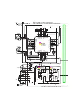
Page 46: ...20 Schematic Diagram for printing with letter size F0305KH 44 ...

Page 47: ...5 0 022 C1030 4V47 R1025 4 7 Q1013 2SC4081STX DC DC CONV Q1012 2SC4081STX DC DC CONV C1038 1 C1034 0 01 C1508 4V22 C1507 0 1 C1506 0 1 R1502 6 8K C1505 5600P C1504 0 47 R1501 1M C1500 6 3V10 C1501 5600P C1502 0 1 C1503 0 1 R1500 6 8K IC1500 C0ZBZ0000515 TONE CONTROL 1 2 3 4 5 6 7 8 16 15 14 13 12 11 10 9 VS IN L TREBLE L BASSI L BASSO L OUT L SDA SCL ALC IN R TREBLE R BASSI R BASSO R OUT R CREF GN...

Page 48: ... COM3 S12 S13 S14 S15 S16 S17 RADIO KEY CDPLAY KEY SELECT2 TCS V DD BUZ CITY MONO DDON TMUTE NC TUNED INT SELECT1 GND4 OSC IN VDD DO VREG BUSY TDATA SO TCLK 6KEY KEY 1 KEY 2 V EE C4 C3 VLCD C2 C1 VDB GND5 X IN X OUT RESET START AC DET VR SCK 2 EMPTY 32 48 AM L R3 1K R4 1K A B Q1308 UN5214TX INTERFACE A C H G I C3 0 01 Z L3 C a Y X W V U T S R Q P O N M L K J I H G F E D B A P F Q P K R D G B C R14...

Page 49: ...P C120 3300P IC302 AK93C45BH L EE PROM 8 7 6 5 1 2 3 4 DO DI CLK CS Vcc NC NC GND R361 1K C321 1 R325 33K M N O a R S T U V W A B C E H I J K L M N Q S U L K a A VREF P 1 2 3 4 5 6 7 8 9 10 11 12 LD MPD NC VC VF VA GND NC VS Vcc VE VB A B C D E F G H I A B C D E F G H I NC R OPTICAL PICK UP SL SV550 GK CIRCUIT DIAGRAM G D S C I F H E G B L Q Z Y R362 100K R354 1K IC303 XC61CN2102MR RESET C302 1 R3...

Page 50: ...P C120 3300P IC302 AK93C45BH L EE PROM 8 7 6 5 1 2 3 4 DO DI CLK CS Vcc NC NC GND R361 1K C321 1 R325 33K M N O a R S T U V W A B C E H I J K L M N Q S U L K a A VREF P 1 2 3 4 5 6 7 8 9 10 11 12 LD MPD NC VC VF VA GND NC VS Vcc VE VB A B C D E F G H I A B C D E F G H I NC R OPTICAL PICK UP SL SV550 GK CIRCUIT DIAGRAM G D S C I F H E G B L Q Z Y R362 100K R354 1K IC303 XC61CN2102MR RESET C302 1 R3...

Page 51: ...S U R X C530 0 1 E O Q19 Q301 C751 1 R751 15K C750 1 R750 15K Q703 XP1210TX VOICE GAIN UP R709 1 2K R713 5 6K R714 5 6K R715 1 2K C712 1 C711 1 R761 1 5K R760 1 5K Q902 XP1210TX MUTING CONT D701 MA111TX Q731 2SC3931CTX SWITCHING IC701 C1BB00000786 HEADPHONE AMP C730 6 3V10 C904 0 1 C9 1 R905 33K Q701 B1ADMB000003 POWER SUPPLY R725 47K R726 2 2K G H I J L R U S C1251 1000P R731 10K C732 4V47 C702 1...

Page 52: ...S U R X C530 0 1 E O Q19 Q301 C751 1 R751 15K C750 1 R750 15K Q703 XP1210TX VOICE GAIN UP R709 1 2K R713 5 6K R714 5 6K R715 1 2K C712 1 C711 1 R761 1 5K R760 1 5K Q902 XP1210TX MUTING CONT D701 MA111TX Q731 2SC3931CTX SWITCHING IC701 C1BB00000786 HEADPHONE AMP C730 6 3V10 C904 0 1 C9 1 R905 33K Q701 B1ADMB000003 POWER SUPPLY R725 47K R726 2 2K G H I J L R U S C1251 1000P R731 10K C732 4V47 C702 1...

Page 53: ...5 0 022 C1030 4V47 R1025 4 7 Q1013 2SC4081STX DC DC CONV Q1012 2SC4081STX DC DC CONV C1038 1 C1034 0 01 C1508 4V22 C1507 0 1 C1506 0 1 R1502 6 8K C1505 5600P C1504 0 47 R1501 1M C1500 6 3V10 C1501 5600P C1502 0 1 C1503 0 1 R1500 6 8K IC1500 C0ZBZ0000515 TONE CONTROL 1 2 3 4 5 6 7 8 16 15 14 13 12 11 10 9 VS IN L TREBLE L BASSI L BASSO L OUT L SDA SCL ALC IN R TREBLE R BASSI R BASSO R OUT R CREF GN...

Page 54: ...5 0 022 C1030 4V47 R1025 4 7 Q1013 2SC4081STX DC DC CONV Q1012 2SC4081STX DC DC CONV C1038 1 C1034 0 01 C1508 4V22 C1507 0 1 C1506 0 1 R1502 6 8K C1505 5600P C1504 0 47 R1501 1M C1500 6 3V10 C1501 5600P C1502 0 1 C1503 0 1 R1500 6 8K IC1500 C0ZBZ0000515 TONE CONTROL 1 2 3 4 5 6 7 8 16 15 14 13 12 11 10 9 VS IN L TREBLE L BASSI L BASSO L OUT L SDA SCL ALC IN R TREBLE R BASSI R BASSO R OUT R CREF GN...

Page 55: ... COM3 S12 S13 S14 S15 S16 S17 RADIO KEY CDPLAY KEY SELECT2 TCS V DD BUZ CITY MONO DDON TMUTE NC TUNED INT SELECT1 GND4 OSC IN VDD DO VREG BUSY TDATA SO TCLK 6KEY KEY 1 KEY 2 V EE C4 C3 VLCD C2 C1 VDB GND5 X IN X OUT RESET START AC DET VR SCK 2 EMPTY 32 48 AM L R3 1K R4 1K A B Q1308 UN5214TX INTERFACE A C H G I C3 0 01 Z L3 C a Y X W V U T S R Q P O N M L K J I H G F E D B A P F Q P K R D G B C R14...

Page 56: ... COM3 S12 S13 S14 S15 S16 S17 RADIO KEY CDPLAY KEY SELECT2 TCS V DD BUZ CITY MONO DDON TMUTE NC TUNED INT SELECT1 GND4 OSC IN VDD DO VREG BUSY TDATA SO TCLK 6KEY KEY 1 KEY 2 V EE C4 C3 VLCD C2 C1 VDB GND5 X IN X OUT RESET START AC DET VR SCK 2 EMPTY 32 48 AM L R3 1K R4 1K A B Q1308 UN5214TX INTERFACE A C H G I C3 0 01 Z L3 C a Y X W V U T S R Q P O N M L K J I H G F E D B A P F Q P K R D G B C R14...

Page 57: ...2BBGE000658 C2FBEB000002 48PIN 80PIN 80PIN 64PIN UN5113TX UN5114TX UN5115TX UN521LTX UN5213TX UN5214TX UN5215TX XP1210TX XP152A12C0MR 2SK1067 4 TL 2SK1958T1 MA111TX MA8120MTX KV1450TL3 4 KV1610STL2 0 MA147TX No 1 No 1 2 3 1 1 6 8 13 14 19 21 26 E C B C B C E B C B C E S D G A Ca A Ca C0ABAA000068 1 3 4 5 2 Anode Cathode Anode Cathode Anode Cathode Anode Cathode Anode Cathode Anode AK93C45BH L 4 5 ...

Page 58: ......
Page 59: ...4 AN22003A NF IC101 SERVO AMP 29 16 LDON NRF DET 8 11 B12 2 OFTR 12 SUBT RFENV NRFDET 3 B3 22 23 FE 15 13 BDO 14 10 19 9 3TENV B3 3TOUT OFTR BDO NRFDET FE IN FE OUT Vcc VREF FBAL TBAL 27 F F E E GCTL PDE PDF PDB LD PD ARF DCDET OFT CONT CEA C A D D B C LDON FO 26 27 FO H BRIDGE1 PRE DRIVER1 FO FO TR TR FBAL VREF VREF TRAVERSE MOTOR M SPINDLE MOTOR SEMICONDUCTOR LASER PHOTO DETECTOR FOCUS COIL TRAC...

Page 60: ...0 2 57 58 80 IOV DD 1 IOV DD 2 29 59 1 DV DD 3V RESET CD NOE 22 A10 8 R ch ICP11 DC IN 4 5V B1 B2 REGB Q11 REGULATOR RESET 25 RESET CD 19 16 MDATA MDATA TCLK TCLK MLD 17 MLD STAT 20 STAT MUTE S202 REST SWITCH REST 31 Vss 30 TDATA 15 INT 12 INT BLKCK 21 BLKCK TDATA 7 PDOWN BUSY 1 BUSY VREF B3 72 V CC B3 71 TREBLE BASS 0 10dB 63dB CONTROL x1 x5 RB I 2 C BUS DECODER LATCHES BASS ALC CONTROL HALF WAVE...

Page 61: ...Y910 R707 R1503 R1504 R1155 R1230 RY906 R731 RY901 R708 R1202 R1231 R905 R1501 R709 R760 R761 R2 R1201 R3 RY1368 R4 R15 R14 R121 R120 R110 R202 R201 R31 R45 R47 R1130 R751 R22 R750 R1159 R1232 R714 R1235 R1218 R1233 R1234 R1170 RY1 R725 R1206 R721 R720 R706 R1240 R1204 R1203 R1521 R1520 R1500 R1502 R1509 R1510 R713 R715 R101 R103 X1301 L1 C507 1 2 3 4 5 IC102 S201 JK11 ON OFF S310 VR1101 L11 L13 L...

Page 62: ...P C120 3300P IC302 AK93C45BH L EE PROM 8 7 6 5 1 2 3 4 DO DI CLK CS Vcc NC NC GND R361 1K C321 1 R325 33K M N O a R S T U V W A B C E H I J K L M N Q S U L K a A VREF P 1 2 3 4 5 6 7 8 9 10 11 12 LD MPD NC VC VF VA GND NC VS Vcc VE VB A B C D E F G H I A B C D E F G H I NC R OPTICAL PICK UP SL SV550 GK CIRCUIT DIAGRAM G D S C I F H E G B L Q Z Y R362 100K R354 1K IC303 XC61CN2102MR RESET C302 1 R3...

Page 63: ...S U R X C530 0 1 E O Q19 Q301 C751 1 R751 15K C750 1 R750 15K Q703 XP1210TX VOICE GAIN UP R709 1 2K R713 5 6K R714 5 6K R715 1 2K C712 1 C711 1 R761 1 5K R760 1 5K Q902 XP1210TX MUTING CONT D701 MA111TX Q731 2SC3931CTX SWITCHING IC701 C1BB00000786 HEADPHONE AMP C730 6 3V10 C904 0 1 C9 1 R905 33K Q701 B1ADMB000003 POWER SUPPLY R725 47K R726 2 2K G H I J L R U S C1251 1000P R731 10K C732 4V47 C702 1...

Reviews: