background image

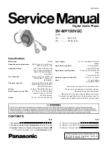
Memory size:

128 MB

Supported sampling frequency:

MP3; 32 kHz, 44.1 kHz, 48 kHz,

WMA; 8 kHz to 44.1 kHz

Supported bit-rates:

MP3 8 kbps to 320 kbps (128
kbps is recommend) WMA 32

kbps to 192 kbps (96 kbps is

recommend)

No. of channels:

Stereo, 2 channels (MUSIC, FM

RADIO) Mono, 1 channel (IC

RECORDER)

Frequency response:

20Hz to 20,000Hz (+0dB, -6dB)

(MUSIC), 300 Hz to 4,300 Hz (IC

RECORDER,HQ mode)

Mic S/N:

30 dB (IC RECORDER,HQ mode)

Radio Frequency range (FM):

87.9 MHz to 107.9MHz (200kHz

steps),87.5 MHz to 108.0 MHz

(50/100 kHz steps),

Output:

4.5 mW + 4.5 mW (16

,M3 jack)

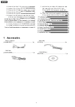
 1 Accessories  

2

 2 Location of Controls 

3

 3 Operation Checks and Component Replacement Procedures  

4

 3.1. 

Removal of the battery cover 

4

©

2005 Matsushita Electric TAIWAN Industrial Co.,

Ltd. All rights reserved. Unauthorized copying and
distribution is a violation of law.

SV-MP100VGC

Colour

(S).......... ......... Silver Type
(D).......... ......... Orange Type

Power supply:

DC 1.5V (one alkaline LR03,AAA

battery)

Approximate play times:

13 hours (MUSIC),

7 hours (FM RADIO)

Approximate recording times:

13 hours (IC RECORDER, HQ

mode)

7 hours (FM RADIO)

Maximum dimensions (WxHxD):

53.2 x 61.1 x 17.5mm

Mass:

41.7g with battery

30.4g without battery


·


Specifications are subject to change without notice.


·


The play times shown depend on operating conditions.


·


Mass and dimensions are approximate.


·


MB means one million bytes. Useable capacity may be less.


·


This product is compatible with the following character code. The

display may not appear correctly with other character codes.

 3.2. 

Removal of the front cabinet 

4

 3.3. 

Removal of the SUB P.C.B. 

4

 3.4. 

Removal of the jack holder 

5

Digital Audio Player

Specifications

CONTENTS

 Page 

Page

TD0502003C3

Summary of Contents for SV-MP100VGC

Page 1: ...Industrial Co Ltd All rights reserved Unauthorized copying and distribution is a violation of law SV MP100VGC Colour S Silver Type D Orange Type Power supply DC 1 5V one alkaline LR03 AAA battery Approximate play times 13 hours MUSIC 7 hours FM RADIO Approximate recording times 13 hours IC RECORDER HQ mode 7 hours FM RADIO Maximum dimensions WxHxD 53 2 x 61 1 x 17 5mm Mass 41 7g with battery 30 4g...

Page 2: ... Cable K1HA05AD0004 1pc 7 1 Install and Copy the software DFU firmware font table After replacing the main PCB and DSP IC main CPU reinstall DFU and firmware and copy font table again 10 7 2 Please contact to the service organization of the belonging for the acquisition of data and obtain the software 10 8 Troubleshooting 14 9 Troubleshooting guide 14 10 Type Illustration of ICs Transistors and Di...

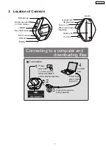
Page 3: ...Earphones jack 3 5 mm stereo USB port HOLD switch Skip search Display back Connection To USB port Small end to player large end to PC Turn the unit on Wait until MODE select display appears Insert so the arrow is facing upwards 1 Press and hold 2 4 3 Connecting to a computer and downloading files MODE 3 SV MP100VGC ...

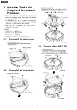
Page 4: ...ement reverse the respective procedures special ressembly procedures are described only when required 3 Select item from the following index when checks or replacement are required Contents 1 Checking for the main P C B 2 Checking for the memory P C B 3 Checking for the LCD ass y 4 Checking for the prevent electrostatic discharge 3 1 Removal of the battery cover 3 2 Removal of the front cabinet 3 ...

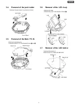
Page 5: ...3 4 Removal of the jack holder 3 5 Removal of the Main P C B 3 6 Removal of the LCD Ass y 3 7 Removal of the LCD holder 5 SV MP100VGC ...

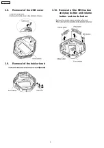
Page 6: ...3 8 Removal of the USB cover 3 9 Removal of the holder knob 3 10 Removal of the REC button and play button and volume button and mode button 6 SV MP100VGC ...

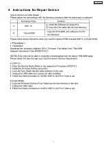
Page 7: ...4 Instructions for Repair Service 7 SV MP100VGC ...

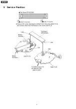
Page 8: ...5 Service Position 8 SV MP100VGC ...

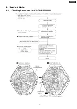
Page 9: ...6 Service Mode 6 1 Checking Procedures for IC3 C2HBZG000008 9 SV MP100VGC ...

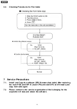
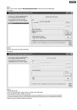
Page 10: ...d Copy the software DFU firmware font table After replacing the main PCB and DSP IC main CPU reinstall DFU and firmware and copy font table again 7 2 Please contact to the service organization of the belonging for the acquisition of data and obtain the software 10 SV MP100VGC ...

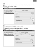
Page 11: ...11 SV MP100VGC ...

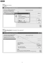
Page 12: ...12 SV MP100VGC ...

Page 13: ...13 SV MP100VGC ...

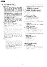
Page 14: ...le disc even when the USB reader writer is connected to the PC this is an indication of an abnormal USB reader writer To confirm this and to improve the accuracy of your service diagnosis however it is recommended that you repeat the check procedure with a new properly functioning USB reader writer If the PC does not operate normally it is not possible to check the problem accurately Be sure to ke...

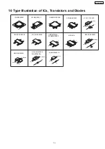
Page 15: ...6 180 45 No 1 No 1 A Ca Anode Cathode B0CCAA000001 A Ca Anode Cathode 4 3 5 2 1 C0DBAGZ0021 4 3 2 1 C0CBCAC00288 UNR921MJ0L B1ABMB00003 D G S B1CFMC000005 D1 D2 S2 S1 G2 MCH6616 G1 B0JDDB000002 Anode Cathode Anode B0ACEM000008 MA2Z74800L B0ZBZ0000070 A Ca Anode A Anode A Ca Anode Cathode LTSTC170CKTP 15 SV MP100VGC ...

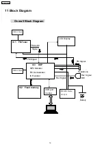
Page 16: ...M Audio Signal FM Signal Rec Signal IC 1 FM Tuner IC3 DSP MP3 Decoder FM Demodulator IC Recoder FM Signal IC2 Flash memory 12MHz Clock USB port Control Headphone MIC DC DC Conv IC 8 9 Battery LCD Display 13MHz Clock Rec Signal 16 SV MP100VGC ...

Page 17: ...BLE BUSMODE SWPORT1 SWPORT1 XTAL1 XTAL2 LIMDEC1 LIMDEC2 TIFC Vref MPXO TMUTE VAFR VAFL PILFIL PHASEFIL GAIN STABILIZTION RESONANCE AMPLIFIER LIMITER DEMODULATOR POWER SUPPLY SOFT MUTE MPX DECODER CRYSTAL OSCILLATOR SOFTWARE PROGRAMMABLE PROT I O MIXER 1st FM AGC N1 2 TUNING SYSTEM VCO IF CENTER FREQUENCY ADJUST LEVEL ADC IF COUNTER MUX Programmable divider output reference frequency divider output...

Page 18: ...ct low Instruction register select LCD_DB 0 LCD_CSB Chip Select T1 T4 P3 N1 N2 T10 V9 F3 C2 B3 C1 C3 D2 D1 D3 E2 E3 F2 G2 HP_OUTL SDAC Left Headphone Output N3 R3 J1 X2 12MHz 15 3 3V VDD D18 ADC_MIC Microphone Input USB_DP Positive USB data line usb 2 0 FS USB_DM Negative USB data line usb 2 0 FS USB_RPU Soft connect output usb 2 0 FS USB_VBUS USB Supply detection line usb 2 0 FS usb 2 0 USB PORT ...

Page 19: ...CE high is ignored and the device does not return to standby mode in program or erase opertion Regarding CE control during read operation refer to Page read section of Device operation CLE COMMAND LATCH ENABLE The CLE input controls the activating path for commands sent to the command register When active high commands are latched into the command register through the I O ports on the rising edge ...

Page 20: ... IC3 C2HBZG000008 V15 MPMC A12 A17 C9 E18 D16 D18 A14 B14 A13 B13 A1 A2 B2 A3 A4 B4 A5 B5 U5 T6 U6 T7 U7 V10 U10 U3 V3 T3 U2 V1 V2 T1 T4 U1 R3 T2 M3 M2 L1 L2 M1 P3 N3 N2 N1 R1 R2 P2 P1 H16 J17 T15 U17 T17 U14 P16 R17 R16 T16 U15 U16 U18 V18 G2 F2 E3 E2 D3 D1 D2 C3 C1 C2 B3 F3 Micro Processor Unit MPU AHB Advanced High Performance Bus Digital Audio Codec Multi Purpose Memory Control Fiash Memory Co...

Page 21: ...ery MP3 position FM position No mark MP3 AND FM position Voltage and signal line Positive voltage line FM RF signal line Audio signal line Mp3 signal line REC signal line Important safety notice Components identified by mark have special characteristic s important for safety Furthermore special parts which have purposes of fire retardant resistors high quality sound capacitors low noise resistors ...

Page 22: ...RCUIT DIAGRAM Schematic diagram 1 R89 1 5K TP55 SUB CIRCUIT A 20 2 1 3 4 5 6 7 8 9 10 11 12 13 14 15 16 17 18 19 24 21 22 23 AAA SIZE LR03 AM 4 BATTERY CN1 C27 4V220 C12 DD3 3V F16 VDD CE F17 Lch Rch USB VCC VCC AD DATA CLOCK G3 Lch Rch F18 C6 G18 H3 Com L44 EXT GND VOUT VDD CE 5 3 4 1 2 C92 4V100 Q10 B1CFMC0005 IC9 C0DBAGZ0021 C93 4V220 C98 K0 1 R13 6 8K SW4 SW5 VOL R14 10K VOL SW6 REC R15 22K R1...

Page 23: ...C N C IC2 C3FBEC000011 FLASH MEMORY 0 0 0 0 0 0 0 3 2 97 2 94 0 0 3 0 0 0 0 3 0 3 0 0 0 0 0 0 0 0 0 0 1 2 0 0 1 2 1 2 1 2 0 0 0 0 3 0 1 2 1 2 1 2 1 2 0 0 0 0 0 0 0 Schematic diagram 2 MAIN CIRCUIT B L48 L41 L73 L58 L40 L39 L7 L10 TP19 R32 0 C29 4V22 C28 K0 1 L53 R34 100K TP13 TP2 TP1 TP9 TP10 D18 TP11 TP12 C100 K390P R18 0 R30 18K D5 1 5V 3 3V R66 4 7K C101 K330P L6 C26 K0 1 C25 4V22 SW1 SW2 SW3 P...

Page 24: ...B_DP USB_DM USB_RPU USB_GNDA USB_VBUS USB_RREF USB_VDDA18_BG USB_VDDA18_PLL USB_VSSA_TEEM USB_VSSA_REF USB_VDDA33 USB_VDDA33 DRV GPIO_3 GPIO_2 GPIO_1 GPIO_0 RSTIN_N DC_DC_PLAY DC_DC_STOP DC_DC_LX2 DC_DC_LX1 DC_DC_VUSB DC_DC_VBAT DC_DC_VOUT33A DC_DC_VOUT33B DC_DC_VOUT18 DC_DC_VSS1 DC_DC_VSS2 DC_DC_GND DC_DC_CLEAN ADC10B_GPA4 ADC10B_GPA3 ADC10B_GPA2 ADC10B_GPA1 ADC10B_GPA0 ADC10B_VDDA33 ADC10B_GMDA ...

Page 25: ...60 K0 1 C61 K0 1 C62 K0 1 C63 K0 1 C64 K0 1 NC CS1 RES A0 WR R W RD E DB0 DB1 DB2 DB3 DB4 DB5 DB6 DB7 VDD VSS VOUT CAP3 CAP1 CAP1 CAP2 CAP2 V0 V1 V2 V3 V4 C86 P S NC D3 E2 E3 F2 G2 V4 U12 T5 U13 U4 19 20 21 22 23 24 SV MP100V CIRCUIT DIAGRAM A B C D E F G H D T4 A B C D E F G H I J K L P3 A14 T1 R73 357K C96 K0 1 430 0mV P P MIC 1 2 3 4 VIN VOUT CE VSS IC8 C72 K0 047 C68 390P R58 2 2K C70 4V100 R5...

Page 26: ... SUB P C B SIDE B A C14 R2 C15 L3 L2 R3 L5 R27 R8 R31 C16 C9 C1 C2 X1 C23 C24 C22 C19 C17 C82 L1 R6 C8 C13 C12 C18 C21 IC6 IC1 D2 L51 L50 L52 S D G To MAIN P C B CN2 C B 15 5 11 10 1 21 20 30 25 40 35 31 R89 C27 C93 C92 C127 R16 C80 Q12 1 2 3 4 5 6 IC9 D11 1 2 3 4 5 Q10 C106 L37 JK1 R15 R13 1AAA SIZE LR03 AM 4 BATTERY 1 5V SW 7 MODE SW 6 REC STOP SW 5 VOL SW 4 VOL HEADPHONE JACK C123 L64 C105 R29 ...

Page 27: ...09 C40 C39 C100 R19 R66 R43 C101 C36 C37 R55 C41 C111 R29 C112 L12 L11 L60 X2 IC3 IC2 L18 C48 C31 L58 L49 C96 R78 L42 C114 IC8 1 2 3 4 LCD MODULE C26 C52 L6 C53 L14 L22 L25 L24 R53 R54 C45 C68 C67 R58 R57 C72 C70 IC10 L23 L20 R76 Q11 C29 R74 C86 C46 C42 C55 C50 R62 R34 D18 D12 D10 E C B 1 2 3 4 R40 C57 C58 C59 C90 C62 C63 C64 C60 C61 R41 C32 CN4 L13 MAIN P C B SIDE B B MAIN P C B SIDE A B To SUB P...

Page 28: ...15 Cabinet Parts Location 28 SV MP100VGC ...

Page 29: ...ng RTL indicates that Retention Time is Limited for this item After the discontinuation of this assembly in production the item will continue to be available for a specific period of time The retention period of availability is dependent on the type of assembly and in accordance with the laws governing part and product retention After the end of this period the assembly will no longer be available...

Page 30: ...OIL T L7 G1A220C00006 POWER INDUCTOR T L10 G1A220C00006 POWER INDUCTOR T L11 J0JBC0000044 CHIP COIL T L12 J0JBC0000044 CHIP COIL T Ref No Part No Part Name Description Remarks L13 J0JBC0000044 CHIP COIL T L14 J0JBC0000044 CHIP COIL T L15 J0JBC0000044 CHIP COIL T L16 J0JBC0000044 CHIP COIL T L18 J0JBC0000044 CHIP COIL T L19 J0JBC0000044 CHIP COIL T L20 J0JBC0000044 CHIP COIL T L21 J0JBC0000044 CHIP...

Page 31: ... C26 K105BJ104KVC CHIP CAPACITOR T C27 F3G0G2270001 TANTALUM CAP T C28 K105BJ104KVC CHIP CAPACITOR T C29 F3E0G2260001 TANTALUM CAP T Ref No Part No Part Name Description Remarks C31 K105BJ104KVC CHIP CAPACITOR T C32 K105BJ104KVC CHIP CAPACITOR T C33 K105BJ104KVC CHIP CAPACITOR T C35 K105BJ104KVC CHIP CAPACITOR T C36 K105BJ104KVC CHIP CAPACITOR T C37 F1G1H180A451 CHIP CAPACITOR T C38 ECST0JZ106R TA...

Reviews: