background image

ORDER  NO.ITD0604020CE

Service Manual

Plasma  Television

TH-50PV600AZ
TH-50PV600H
TH-50PV600M
TH-50PV600MT

GP9DE  Chassis

Power Source


Power  Consumption


Average  use


Standby  condition


Plasma  Display  panel


Drive  method


Aspect  Ratio


Contrast  Ratio


Visible  screen  size


(No.  of  pixels)

Sound

Speaker


Audio  Output


Headphones


PC  signals

Receiving  Systems/


Band  Name


(PV600AZ)

AC  220-240  V,  50/60  Hz

448  W

0.3  W

AC  type


16:9

Max  10000:1


127  cmV

1,106  mm  (W)  x  622  mm  (H)  x  1,269  mm  (diagonal)

1,049,088  (1,366  (W)  x  768  (H))  [4,098  x  768  dots]

Woofer  ( Ф 80  mm)  x  2  pcs,  Tweeter  (23  mm  x  Ю0  mm)  x  2pcs


31  W  [15.5  W  +  15.5  W]  (10  %  THD)

M3  (3.5  mm)  Jack  x  1


VGA,  SVGA,  XGA

SXGA.... (compressed)

Horizontal  scanning  frequency  31-69  kHz


Vertical  scanning  frequency  59-86  Hz

1.  PAL B/G

Reception of Off air broadcasts

2.  NTSC 4.43
3.  NTSC 3.58
4.  PAL 60Hz

Playback from Video Tape Recorders
Playback from Special Video Tape Recorders and Special Video Disc Players 
(Via the AV Sockets) only.

Panasonic

©  2006  Matsushita  Electric  Industrial  Co.,  Ltd.  All


rights 

reserved. 

Unauthorized 

copying 

and


distribution  is  a  violation  of law.

Summary of Contents for TH-50PV600AZ

Page 1: ... 106 mm W x 622 mm H x 1 269 mm diagonal 1 049 088 1 366 W x 768 H 4 098 x 768 dots Woofer Ф80 mm x 2 pcs Tweeter 23 mm x Ю0 mm x 2pcs 31 W 15 5 W 15 5 W 10 THD M3 3 5 mm Jack x 1 VGA SVGA XGA SXGA compressed Horizontal scanning frequency 31 69 kHz Vertical scanning frequency 59 86 Hz 1 PAL B G Reception of Off air broadcasts 2 NTSC 4 43 3 NTSC 3 58 4 PAL 60Hz Playback from Video Tape Recorders Pl...

Page 2: ... Players and Special VCR s or DVD 16 PAL 60 Hz 6 0 MHz 17 PAL 60 Hz 6 5 MHz VHF 0 to 12 UHF 21 to 69 S 1 to S 3 S1 to S41 VHF BAND 2 12 PAL SECAM B K1 0 12 PAL BAUST 1 9 PAL B N Z 1 12 PAL SECAM D 1 12 NTSC M Japan 2 13 NTSC M USA V H F U H F 0 C 4 0 C 20 80 RH non condensing RCA PIN Type x 2 RCA PIN Type x 1 Mini DIN 4 pin RCA PIN Type x 2 RCA PIN Type x 1 Y PB CB PR CR RCA PIN Type x 2 RCA PIN T...

Page 3: ...Remove the C2 Board 15 6 22 Remove the C3 Board 15 6 23 Remove the stand brackets 16 6 24 Remove the C4 Board 16 6 25 Remove the C5 Board 16 6 26 Remove the C6 Board 16 6 27 Remove the front bracket 17 6 28 Remove the G Board GK Board and GS Board 17 6 29 Remove the S Board 17 6 30 Remove the GS Board and SD Module 17 6 31 Remove the Plasma panel section from the Front frame glass 18 6 32 Remove t...

Page 4: ... D Board 5of 8 SchematicDiagram 106 14 35 D Board 6of 8 SchematicDiagram 107 14 36 D Board 7 of 8 Schematic Diagram 108 14 37 D Board 8 of 8 Schematic Diagram 109 14 38 C1 C2 C5 and C6 Block Diagram 110 14 39 C3 C4 SS SS2 and SS3 Board Block Diagram 111 14 40 C1 Board 1 of 2 Schematic Diagram 112 14 41 C1 Board 2 of 2 Schematic Diagram 113 14 42 C2 Board 1 of 3 Schematic Diagram 114 14 43 C2 Board...

Page 5: ...75 60 00 1 080i 50 Hz 28 13 50 00 1 080i 50 Hz 1 31 25 50 00 640 x 400 70 Hz 31 46 70 07 640 x 480 60 Hz 31 47 59 94 640 x 480 75 Hz 37 50 75 00 800 x 600 60 Hz 37 88 60 32 800 x 600 75 Hz 46 88 75 00 800 x 600 85 Hz 53 67 85 06 1 02 4 x7 68 60 Hz 48 36 60 00 1 02 4 x7 68 70 Hz 56 48 70 07 1 02 4 x7 68 75 Hz 60 02 75 03 1 02 4 x7 68 85 Hz 68 68 85 00 1 280 x 1 024 60 Hz 63 98 60 02 Macintosh13 640...

Page 6: ...ach point 5 Reserve the AC plug in the AC outlet and repeat each of the above measure 6 The potential at any point TOUGH CURRENT expressed as voltage Ui and U2 does not exceed the following values For a c Ui 35 V peak and U2 0 35 V peak For d c Ui 1 0 V Note The limit value of U2 0 35 V peak for a c and U1 1 0 V for d c correspond to the values 0 7 mA peak a c and 2 0 mA d c The limit value U1 35 ...

Page 7: ...s anti static ESD protected can generate electrical charge sufficient to damage ES devices 5 Do not use freon propelled chemicals These can generate electrical charges sufficient to damage ES devices 6 Do not remove a replacement ES device from its protective package until immediately before you are ready to install it Most replacement ES devices are packaged with leads electrically shorted togeth...

Page 8: ... a higher melting point than standard solder Typically the melting point is 50 70 F 30 40 C higher Please use a high temperature soldering iron and set it to 700 20 F 370 10 C Pb free solder will tend to splash when heated too high about 1100 F or 600 C If you must use Pb solder please completely remove all of the Pb free solder on the pins or solder areabefore applying Pb solder If this is not pr...

Page 9: ... Lower Left TA Tuner C5 Data Driver Lower Center DG Digital Signal Processor Micom HDMI Interface C6 Data Driver Lower Right D Format Converter Plasma Ai Sub Field Processor SC Scan Drive HC Jig Connection SU Scan out Upper K Remote receiver Power LED SD Scan out Lower S Power Switch SS Sustain Drive G Front Terminal SS2 Sustain Connector Upper GK Key Switch SS3 Sustain Connector Lower GS SD Card ...

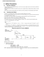
Page 10: ...d remove the fans 6 3 Remove the Speaker box ass y left 1 Unlock the cable clampers to free the cable 2 Disconnect the relay coupler 3 Remove the Speaker box ass y left 6 4 Remove the Speaker box ass y right 1 Unlock the cable clampers to free the cable 2 Disconnect the relay coupler 3 Remove the Speaker box ass y right 6 5 Remove the rear terminal cover 1 Remove the screws x8 x5 x2 4 2 Remove the...

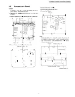
Page 11: ...P25 2 Remove the screws 6 and remove the P Board unit P25 P10 P23 P5 P11 P2 6 6 Remove the P Board 3 Remove the screws x9 on the back side 4 Remove the screws 5 5 Remove the molding props x8 6 Remove the P Board Note When assembling the P Board the position of each hole of the insulation sheets A and B is set to the position of each hole of the P Board then assemble them marks indicate setting pos...

Page 12: ...ard РАЗЗ PA31 PA32 РАЮ PA1 PA2 PA5 PA Board 6 8 Remove the tuner unit 1 Unlock the cable clampers to free the cable 2 Disconnect the couplers DG5 G51 GS52 PA40 and earth cable 3 Disconnect the flexible cables DG3 and PA20 4 Remove the screws 4 remove the tuner unit 1 Disconnect the coupler DG2 2 Disconnect the flexible cables DG1 DG15 and DG20 3 Remove the screw 7 remove the DG Board DG3 DG5 DG22 ...

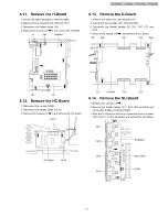
Page 13: ...connect the flexible cable HC15 3 Remove the screws 2 and remove the HC Board 1 Remove the tuner unit See section 6 6 2 Disconnect the couplers D5 D20 and D25 3 Disconnect the flexible cables D3 D31 D32 D33 and D34 4 Remove the screws x4 and remove the D Board D5 D20 D31 D32 D25 6 14 Remove the SU Board 1 Remove the screws 3 2 Remove the flexible cables SU1 SU2 SU3 and SU4 and remove the bridge co...

Page 14: ... SC42 SD42 on the SC Board and remove the SD Board 6 16 Remove the SC Board 1 Unlock the cable clampers to free the cable 2 Disconnect the couplers SC2 SC20 and SC23 3 Remove the screws x9 and remove the SC Board 1 Disconnect the coupler SS23 and disconnect the flexible cable SS55 2 Remove the screws 2 and remove the SS2 Board 6 18 Remove the SS3 Board 1 Disconnect the coupler SS22 and disconnect ...

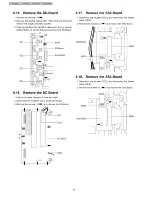
Page 15: ...2 Disconnect the flexible cables CA1 CA2 and CA3 3 Disconnect the flexible cable C10 4 Remove the screws 5 and remove the C1 Board 1 Remove the flexible cables holder fastening screws 8 2 Disconnect the flexible cables CA4 CA5 CA6 and CA7 3 Disconnect the flexible cables C20 C21 and C22 4 Remove the screws x5 and remove the C2 Board C20 C2 Board C21 6 22 Remove the C3 Board 1 Remove the flexible c...

Page 16: ...ws 8 3 Disconnect the flexible cables CB8 CB9 CB10 and CB11 4 Disconnect the flexible cables C41 and C42 5 Disconnect the couplers C43 and C44 6 Remove the screws x5 and remove the C4 Board 1 Remove the flexible cables holder fastening screws 8 2 Disconnect the flexible cables CB4 CB5 CB6 and CB7 3 Disconnect the flexible cables C50 C51 and C52 4 Remove the screws 5 and remove the C5 Board C50 C5 ...

Page 17: ...ront bracket See section 6 28 2 Remove the screws x3 and remove the front side metal frame 3 Remove the screws 3 and disconnect the couplers G3 GK3 4 Remove the G Board and GK Board 1 Disconnect the coupler S1 2 Remove the screws 2 and remove the S Board metal frame 3 Remove the screws x2 and remove the S Board 6 30 Remove the GS Board and SD Module 1 Remove the stand bracket R See section 6 24 2 ...

Page 18: ... screw 1 9 Remove the GS Board and SD Module 6 31 Remove the Plasma panel section from the Front frame glass 1 Remove the front frame and the plasma panel fastening screws x12 2 Remove the front frame and the stand brackets fastening screws x2 3 For leaving the plasma panel from the front frame pull the bottom of the front frame forward lift and remove 18 ...

Page 19: ...rews 2 5 Remove the squawker speaker 1 Remove the front frame See section 6 32 2 Remove the glass holder R and L See section 6 33 3 Remove the screws хЗ 4 Remove the bottom shield 5 Remove the screws 5 6 Remove the glass holder bottom R and L 7 Remove the screws x9 8 Remove the glass holder bottom Glass holder R Glass holder bottom Glass holder L 9 Remove the screws 2 10 Disconnect the couplers K1...

Page 20: ...nect the flexible cables x22 from the Plasma panel to the C1 C2 C3 C4 C5 and the C6 Board and fit the flexible cable holders 3 Attach the Hooks left right and fit the stand brackets L R to the new plasma panel 4 Place the plasma panel section on the servicing stand 5 Attach the front frame and each P C Board and so on to the new plasma panel When fitting the front frame be careful to allow any deb...

Page 21: ...TH 50PV600AZ TH 50PV600H TH 50PV600M TH 50PV600MT 7 Location of Lead Wiring 7 1 Lead of Wiring 1 21 ...

Page 22: ... TH 50PV600AZ TH 50PV600H TH 50PV600M TH 50PV600MT 7 2 Lead of Wiring 2 22 ...

Page 23: ...I TH 50PV600AZ TH 50PV600H TH 50PV600M TH 50PV600MTI 7 3 Lead of Wiring 3 23 ...

Page 24: ...I TH 50PV600AZ TH 50PV600H TH 50PV600M TH 50PV600MTI 7 4 Lead of Wiring 4 24 ...

Page 25: ...I TH 50PV600AZ TH 50PV600H TH 50PV600M TH 50PV600MTI 7 5 Lead of Wiring 5 25 ...

Page 26: ... OPTION8 40 I ________ OPTION9 FF OPTIONIO 6F OPTION11 4E OPTION12 09 OPTION13 00 CHECK D8 ____________________ i PANEL MCU 01 00 IPANEL EEPROM 30 08 IPANEL FPGA 40 22 pan el p d r o m 30 08 Factory use only Option Code display The numbers are displayed in hexadecimal Note Option Codes are only examples Please refer the option table for each models Software Version If the CCU ports have been check...

Page 27: ... Subject Information of LED Flashing timing chart 2 Contents When an abnormality has occurred the unit the protection circuit operates and reset to the stand by mode At this time the defective block can be identified by the number of blinkes of the Power LED on the front panel of the unit 27 ...

Page 28: ...00H TH 50PV600M TH 50PV600MTI 8 2 No Power I First check point There are following 2 states of No Power indication by power LED 1 No lit 2 Green is lit then turns red blinking a few seconds later See 8 1 3 Only red is lit 28 ...

Page 29: ...I TH 50PV600AZ TH 50PV600H TH 50PV600M TH 50PV600MTI 8 3 No Picture 29 ...

Page 30: ...on the screen Fig 1 is the possible defect P C B for each local area C3 board D board Л V C2 board D board л V C1 board D board A _ _ _ _ _ _ _ _ _ _ Y C4 board D board _A_ Y C5 board D board _A_ Panel Thin vertical line Local screen failure chart Fig 1 SU board SC board У SS board D board SD board Y C6 board D board 30 ...

Page 31: ...djusted by remote control in Service Mode 9 1 How to enter SERVICE 1 1 In sound menu set BASS to MAXIMUM and set TREBLE to MINIMUM 2 Simultaneously press INDEX button on remote control and DOWN button V on the TV set 9 2 How to enter SERVICE 2 1 Set the channel to CH99 2 Select the EQ 12kHz 3 Press HOLD button on remote control Note To exit to Service mode press EXIT or Power button on remote cont...

Page 32: ...TH 50PV600AZ TH 50PV600H TH 50PV600M TH 50PV600M T 32 ...

Page 33: ...b4 0 1 0 User aspect 14 9 enable 1 b5 0 0 0 ALBD 14 9 14 9 enable Zoom3 disable at self wide 1 Zoom l Zoom3 enable at self wide 0 b6 1 1 1 TEXT enable 1 b7 0 1 0 TEXT TOP TOP enable 1 option5 3B 3B 3B bO 1 1 1 CH Blanking Blanking enable 1 Ы 1 1 1 AV Blanking Blanking enable 1 b2 0 0 0 Noise mute Noise mute enable O b3 1 1 1 sub picture without sub picture O with sub picture l b4 1 1 1 2tuner 2tun...

Page 34: ...7 0 1 0 HDMI AVI Aspect enable 1 option11 4F 4F 4F Additional bO 1 1 1 Remocon Type Delux 1 Leader O Ы 1 1 1 Environment Al PDP enable with viewing mode auto 1 disable without viewing mode auto 0 b2 1 1 1 WSS14 9 off WSS 14 9 off 1 b3 1 1 1 Child lock Child Lock on Tuning Menu skip 1 b4 0 0 0 b5 0 0 0 Contrast Al enable 1 b6 1 1 1 Service H POS enable 1 b7 0 0 0 Service V VOS enable 1 option12 21 ...

Page 35: ...scn voltage should be performed after confirmation of Vad adjustment When Vad 105V Voltage of Vscn is 35V 4V 10 1 2 Adjustments Adjust driver section voltages referring the panel data on the panel data label Check or adjust the following voltages with the multimeter Name Test Point Voltage Volume Remarks Vsus TPVSUS SS Vsus 2V VR251 P Ve TPVE SS Ve 2V VR6000 SS Vset TPVSET SC 280V 7V Fixed Vad TPV...

Page 36: ...uit Board exchange 10 3 1 Caution 1 To remove P C B wait 1 minute after power was off for discharge from electrolysis capacitors 10 3 2 Quick adjustment after P C B exchange Adjust the following voltages with the multimeter P C B Name Test Point Voltage Volume Remarks P Board Vsus TPVSUS SS Vsus 2V VR251 P SC Board Vad TPVAD SC 105V 1V VR6600 SC SS Board Ve TPVE SS Ve 2V VR6000 SS D DG Board White...

Page 37: ...ITH 50PV600AZ TH 50PV600H TH 50PV600M TH 50PV600MTI 10 4 10 5 Adjustment Volume Location Test Point Location 37 ...

Page 38: ... the Service1 mode 4 Select G CUTOFF item using the color key Red or Green and set to 128 using the color key Yellow or Blue Also B CUTOFF and R CUTOFF set to 128 5 Set G DRIVE at 208 6 Touch the signal receiver of color analyzer to the highlight window s center and adjust B drive and R drive so x y become the Color balance Cool in the below table 7 Set ALL DRIVE to 252 8 Set colorbalance to STAND...

Page 39: ...lue Also B CUTOFF and R CUTOFF set to 128 5 Set G DRIVE at 208 6 Touch the signal receiver of color analyzer to the highlight window s center and adjust B drive and R drive so x y become the Color balance Cool in the below table 7 Set ALL DRIVE to 252 8 Set colorbalance to Standard 9 Fix G cutoff B cutoff and R cutoff at 128 10 Fix G drive at 208 11 Adjust B drive and R drive so the highlight wind...

Page 40: ...a dark room Complete the adjustment within 10 minutes after the turn on electricity Turn on the power supply again when it is not possible to complete it by aging etc 1 Display the 10 steps gray scalepattern for adjusting subbright from video input 2 Use Sub Bright in the Sevice1 mode to adjust so the 6th section shows up and the 7th fades away Picture menu Dynamic Color balance Normal ASPECT 16 9...

Page 41: ...d screen size at 16 9 Component input dynamic standard 1 Connect the set s AC power to the wattmeter 2 Input the signal top half color bar Bottom half Horizontal 10steps bar 3 Select the PWRCTL item in the Service1 mode 4 Adjust PWRCTL so the set s power consumption is 438 10W Remarks 1 The initial data are Data address A0 0102 Default data 0x00 2 The power and data are in reverse relationship Low...

Page 42: ...it Colour bar shown as below 100 White 2 Goes into service mode choose Sub Contrast and it checks that data value is 512 It checks that an initial value is a default Adjustment of RF system Remarks 1 The colour key yellow button of remote control is pushed 2 The OSD character of sub contrast becomes red Inside under automatic adjustment 3 The OSD character of sub contrast returns to white 4 End Pr...

Page 43: ...ice mode choose VIDEO Gain2 and check that data is 255 Check that initial value is the default Adjustment Remarks 1 Check the brightness of main screen and sub screen by watching 2 Go to procedure 3 when the brightness of sub screen is higher than that of main screen Oppositely do not adjust and end when the brightness of sub screen is lower than that of main screen 3 Adjust VIDEO Gain2 so that th...

Page 44: ...ta of EEPROM ADDRESS 0BAF to 00 Next Push the Power switch button off on the set the remote control to turn the set off on Then it is no longer hotel mode 4 Access command to the Hotel mode setup menu Prerequisite It is conditions that the data of EEPROM ADDRESS 0BAF is 01 In order to display the Hotel mode setup menu please enter the following command within 2 second I TVl down REMOTE1 TV AV 3 ti...

Page 45: ...600AZ TH 50PV600H TH 50PV600M TH 50PV600Mt 13 Conductor Views 13 1 P Board P BOARD FOIL SIDE ETXMM610MEF TH 50PV600AZ H M MT P BOARD ETXMM610MEF A I TH 50PV600AZ H M MT P BOARD ETXMM610MEF 1 1 B 6 5 4 3 2 1 45 ...

Page 46: ...05 C 4 Q104 H 2 IC501 B 3 PC506 H 4 Q106 H 2 Q301 H 3 MODULE VOLUME Q302 G 3 MC101 G 3 VR251 C 5 Q351 F 5 MC201 C 3 VR351 F 4 Q352 G 5 MC202 D 3 VR401 E 5 Q353 F 5 MC301 F 3 Q354 F 4 MC502 C 2 Q401 F 4 MC601 C 4 Q402 G 4 MC701 H 5 Q403 E 4 Q404 G 5 Q405 F 5 Q406 E 4 Q501 B 3 Q502 B 3 Q551 G 5 Q552 G 6 Q553 G 6 TH 50PV600AZ H M MT P BOARD PARTS LOCATION ...

Page 47: ...C503 G 4 VR251 H 5 IC401 E 5 PC505 G 4 VR351 D 4 IC501 H 3 PC506 B 4 VR401 E 5 MODULE TRANSISTOR MC101 C 3 Q301 C 3 MC201 G 3 Q302 C 3 MC202 E 3 Q401 E 5 MC301 D 3 Q402 D 4 MC502 G 2 Q404 C 5 MC601 G 4 Q405 D 5 MC701 B 5 Q501 H 3 TH 50PV600AZ H M MT P BOARD PARTS LOCATION 46 ...

Page 48: ... TH 50PV600AZ TH 50PV600H TH 50PV600M TH 50PV600MT P BOARD COMPONENT SIDE ETXMM610MEF TH 50PV600AZ H M MT P BOARD ETXMM610MEF A I TH 50PV600AZ H M MT P BOARD ETXMM610MEF 1 1 B H 6 5 4 3 2 1 47 ...

Page 49: ...TH 50PV600AZ I TH 50PV600H I TH 50PV600M I TH 50PV600MT 13 2 PA Board PA BOARD FOIL SIDE TNPA3761AE TH 50PV600AZ H M MT PA BOARD TNPA3761AE A I В 48 ...

Page 50: ... TP5613 B 1 IC5602 F 4 TP5615 B 1 IC5611 D 4 TP5616 A 1 TP5617 B 1 TRANSISTOR TPFSOS B 1 TPM5 F 2 Q2306 B 3 TPM9 F 2 Q2307 A 2 TPM18 E 3 Q2308 C 3 TPM33 E 4 Q2309 B 3 TPMUTE D 1 Q5606 E 3 TPS5 E 2 TPS9 E 3 TPS33 D 2 TPSSOS A 1 TPSTB5V D 1 TH 50PV600AZ H M MT PA BOARD TNPA3761AE F I G I H I j ...

Page 51: ...V C 5 IC2303 E 4 Q2303 E 3 TPM18V B 3 IC2304 E 2 Q2304 D 3 TPM33V B 2 IC2305 D 3 Q2305 E 3 TPS5V C 1 IC5601 B 2 Q5601 A 3 TPS9V C 2 IC5602 A 3 Q5602 A 3 TPS33V C 2 IC5604 C 2 Q5603 A 1 IC5611 C 4 Q5604 C 3 IC5801 C 5 Q5605 A 2 Q5608 C 4 Q5609 C 4 Q5610 C 3 Q5612 B 1 Q5613 A 1 Q5641 C 3 Q5642 C 3 Q5643 C 3 Q5644 C 3 Q5653 C 4 TH 50PV600AZ H M MT PA BOARD TNPA3761AE A I TH 50PV600AZ H M MT PA BOARD ...

Page 52: ... 3 7 6 8 _ T A SEE REVERSE FOR SUFFIX bmsw1sw2 TU001 I T a T T A T i i JS027 ю н н н и н н п 5 ____________________ 0 Л F S 0 r L o o07 7 25_o022 J 10 04 n C r 0 1 1 T A 8 I J 1 HC BOARD FOIL SIDE TNPA3852 H H 2 1 PbF I l i u m 11 TH 5 PV6 AZ H M MT H BOARD TNPA376 TH 50PV600AZ H M MT HC BOARD TNPA3852 A I B TH 50PV600AZ H M MT TA BOARD TNPA3768AB 1 C I D TH 50PV600AZ H M MT H BOARD TNPA376 TH 5 P...

Page 53: ...3209 E 2 102109 0 2 Q2105 F 4 Q3008 G 3 Q3210 E 2 I02210 0 1 Q2106 E 2 Q3011 0 4 Q3331 B 5 I03005 D 3 Q2107 F 2 Q3012 0 4 Q3332 0 5 I03200 F 2 Q2108 E 2 Q3013 0 4 Q3333 0 5 I03301 0 5 Q2109 F 2 Q3014 0 4 Q5614 F 2 I05603 G 2 Q2113 G 4 Q3015 0 4 Q2114 G 3 Q3017 0 4 h F1 Гт л 1 TA BOARD COMPONENT SIDE TNPA3768AB HC BOARD COMPONENT SIDE TNPA3852 TH 50PV600AZ H M MT H BOARD TNPA3760 TH 50PV600AZ H M M...

Page 54: ...0PV600AZ TH 50PV600H TH 50PV600M TH 50PV600MT 13 4 6 5 4 3 2 1 G Board G BOARD FOIL SIDE TNPA3764AF G BOARD COMPONENT SIDE TH 50PV600AZ H M MT G BOARD TNPA3764AF B TH 50PV600AZ H M MT G BOARD TNPA3764AF H 52 ...

Page 55: ...NPA3762AE K BOARD COMPONENT SIDE TNPA3762AE r TNPA3762 R2573 D ц П 1 П Л Л 12 1о 3 GK BOARD FOIL SIDE TNPA3848AD C2510 R2512 GK BOARD COMPONENT SIDE TNPA3848AD TH 50PV600AZ H M MT GK BOARD TNPA3848AD K BOARD TNPA3762AE S BOARD TNPA3763AC A I В ...

Page 56: ...0PV600AZ TH 50PV600H TH 50PV600M ТН 50РУ600МТ S BOARD FOIL SIDE TNPA3763AC S BOARD COMPONENT SIDE TNPA3763AC TH 50PV600AZ H M MT GK BOARD TNPA3848AD K BOARD TNPA3762AE S BOARD TNPA3763AC 1 I F I G I H I i 53 ...

Page 57: ...Q4067 Q4068 Q4069 Q4070 Q4071 Q4073 Q4074 Q4075 Q4076 Q4077 Q4078 Q4079 Q4082 Q4083 Q4084 Q4918 Q4919 C 2 A 3 A 3 D 2 A 2 A 2 B 2 B 2 B 1 B 1 A 2 B 3 B 2 B 3 B 3 B 1 A 3 B 3 B 2 B 2 B 1 E 2 E 2 TP TP1101 F 3 TP1102 F 3 TP1103 F 2 TP1104 F 2 TP1105 F 2 TP1 106 F 2 TP1 107 F 2 TP1 113 C 5 TP1 114 B 5 TP1 115 D 5 TP1 116 D 5 TP1 117 C 5 TP1 118 D 5 TP1 119 D 5 TP1120 F 3 TP4028 B 4 TP4029 B 3 TP4030 ...

Page 58: ...E 3 Q1115 A 2 Q4081 F 4 IC4014 D 1 Q1116 B 2 IC4019 F 4 Q1121 C 2 TP IC4020 D 3 Q1130 D 2 IC4022 F 2 Q1131 D 2 TP1 108 A 4 IC4023 F 1 Q1132 C 2 TP1109 A 5 IC4025 F 3 Q1133 C 2 IC4026 F 2 Q1142 C 1 IC4027 E 1 Q1143 C 1 IC4028 F 3 Q4040 E 2 IC4032 D 5 Q4041 E 1 IC4033 F 5 Q4042 E 2 IC4034 D 4 Q4043 E 2 IC4035 E 4 Q4044 E 2 IC4036 B 4 Q4046 E 2 IC4037 D 4 Q4050 F 5 IC4038 E 4 Q4051 D 1 IC4039 C 4 Q40...

Page 59: ...E 2 IC9002 F 5 Q9401 C 2 IC9011 G 2 Q9402 D 2 IC9602 C 4 Q9500 A 3 IC9800 A 3 Q9800 G 2 IC9801 E 4 Q9801 G 2 IC9806 A 3 Q9803 F 4 IC9807 B 4 Q9805 F 4 IC9809 A 2 Q9806 E 4 TRANSISTOR TP Q9044 F 3 TP442 C 1 Q9045 G 3 TP9000 E 3 Q9048 F 3 Q9049 E 2 Q9050 E 3 Q9057 F 2 Q9058 F 2 Q9060 F 3 TH 50PV600AZ H M MT D BOARD TZTNP01BETB A I B TH 50PV600AZ H M MT D BOARD TZTNP01BETB и 1 1 56 ...

Page 60: ...9007 B 3 Q9047 A 3 IC9200 C 4 Q9051 E 2 IC9300 F 3 Q9052 E 2 IC9301 E 2 Q9053 D 2 IC9304 E 4 Q9054 D 2 IC9400 D 3 Q9100 D 3 IC9401 C 2 Q9301 E 4 IC9402 B 4 Q9302 E 4 IC9500 B 4 IC9503 B 3 TP IC9504 B 5 TP443 E 3 IC9505 C 3 TP444 E 3 IC9603 B 3 IC9802 B 3 IC9803 A 3 6 5 4 3 2 1 TH 50PV600AZ H M MT D BOARD TZTNP01BETB B TH 50PV600AZ H M MT D BOARD TZTNP01BETB H 57 ...

Page 61: ...ITH 50PV600AZ TH 50PV600H TH 50PV600M TH 50PV600MT 13 8 C1 Board Parts Location C1 BOARD IC 6 IC71 01 5 C1 BOARD FOIL SIDE TNPA3821 4 3 C1 BOARD COMPONENT SIDE TNPA3821 58 ...

Page 62: ... IC7208 D 1 IC7209 E 1 5 C2 BOARD FOIL SIDE TNPA3822 4 3 C2 BOARD COMPONENT SIDE TNPA3822 2 Г 2 2 2 I 3 6 s 1 r r A 1 R 2 2 4 d jr Ц J i i s i з 2 2 8 i a u 9 M S f l i f l l P Q I i Ц6 11a 1 1 11 t Z S T AA11 1 2 3 9 E a C R N O 7 0 а 0 а л в 0 0 В TNPA3S22 I Q ГСП jS 7 ORDER NO 1 TH 50PV600AZ H M MT C2 BOASD TNPA3S22 A I B TH 50PV600AZ H M MT C2 BOARD TNPA3822 и 1 i 59 ...

Page 63: ...00MT 13 10 C3 Board 6 5 C3 BOARD IC IC7301 B 1 IC7302 A 2 IC7303 B 2 IC7304 B 2 IC7305 B 1 C3 BOARD FOIL SIDE TNPA3823 4 3 C3 BOARD COMPONENT SIDE TNPA3823 2 1 TH 50PV600AZ H M MT C3 BOASD TNPA3823 A I B TH 50PV600AZ H M MT C3 BOASD TNPA3823 h 1 60 ...

Page 64: ...4 C4 BOARD COMPONENT SIDE TNPA3824 C4 BOARD IC IC7401 B 2 IC7402 A 2 IC7403 B 2 IC7404 C 2 IC7405 C 2 o n Щ Ц Ш Ш С а ш йтез в ш C R N O 7 TNPA3824 Щ r n 0 Ш 4 ORDER NO r n m C 7 III C 4 4 _l X TH 50PV600AZ H M MT C4 BOASD TNPA3S24 A TH 50PV600AZ H M MT C4 BOASD TNPA3S24 1 i B H 6 5 4 3 2 1 61 ...

Page 65: ...PA3825 C5 BOARD IC IC7501 H 1 IC7502 E 2 IC7503 F 2 IC7504 G 2 IC7505 G 2 IC7506 I 2 IC7507 D 2 IC7508 D 2 IC7509 E 2 з и C5 BOARD COMPONENT SIDE TNPA3825 т е 0 ф Г в ц в 1 в J L a i i r i j TH 50PV600AZ H M MT C5 BOARD TNA3S25 A TH 50PV600AZ H M MT C5 BOARD TNA3S25 1 B H 6 5 4 3 2 1 62 ...

Page 66: ...MM1 Parts Location C6 BOARD IC TNPA3826 CRNO 7 LC6 о _l_ Г o П s R601 R603 0 г Г Z0 1 L I 5 _________3 5R C626 JC627 L П ___________________________ m D606 C620 S S C624 D605 I f A и Д И Ё м P J I ______________________ е Г L TH 50PV600AZ H M MT C6 BOARD TNPA3826 A T TH 50PV600AZ H M MT 6 BO AR D TNPA3826 1 i B H 6 IC7601 5 4 3 2 1 63 ...

Page 67: ...ITH 50PV600AZ TH 50PV600H TH 50PV600M TH 50PV600MT 13 14 SC Board 6 SC BOARD FOIL SIDE TNPA3827 5 4 3 2 1 TH 50PV600AZ H M MT SC BOARD TNPA3827 A I B TH 50PV600AZ H M MT SC BOARD TNPA3827 и 1 1 64 ...

Page 68: ...22 TP23 TP24 TP25 TP26 TP27 TP28 TP29 TP30 TP31 TP32 TP33 TP34 TP35 TP38 TP39 TP40 B 2 B 2 A 2 A 2 A 3 A 3 B 3 A 3 G 1 G 2 G 1 H 2 G 1 H 2 H 2 H 2 H 2 H 1 G 2 H 2 H 2 G 2 G 1 G 1 G 2 G 1 H 2 I 4 I 5 F 5 B 5 A 3 E 2 D 3 H 2 G 2 D 5 TP41 TP42 TP43 TP44 TP45 TP46 TP47 TP48 TP49 TP50 TP51 TP52 TP53 TP54 TP55 TP56 TP59 TP60 TP61 TP62 TP63 TP64 TP65 TP67 TP68 VOLUME VR6600 VR6601 VR6602 D 5 D 5 D 5 D 5 ...

Page 69: ...Q6423 Q6441 Q6442 Q6443 Q6451 Q6452 Q6453 Q6471 Q6511 Q6512 Q6516 Q6517 Q6531 Q6532 Q6551 Q6552 Q6581 B 4 A 4 A 4 A 4 I 4 C 4 I 4 B 4 A 2 TRANSISTOR D 4 E 4 E 4 G 4 H 4 H 4 E 2 F 2 F 2 F 2 F 2 G 2 B 3 F 4 E 4 G 4 G 4 E 2 F 2 F 2 F 2 E 2 Q6601 Q6602 Q6621 Q6622 Q6641 Q6642 Q6643 Q6644 Q6645 Q6646 Q6647 Q6648 Q6662 Q6671 Q6672 Q6673 Q6680 Q6681 Q6682 Q6742 Q6743 Q6744 Q6762 Q6781 Q6782 Q6791 Q6803 Q...

Page 70: ...TH 50PV600AZ TH 50PV600H TH 50PV600M TH 50PV600MT SC BOARD COMPONENT SIDE TNPA3827 TH 50PV600AZ H M MT SC BOARD TNPA3827 A T TH 50PV600AZ H M MT SC BOARD TNPA3827 1 1 B H 6 5 4 3 2 1 66 ...

Page 71: ... Board SU BOARD FOIL SIDE TNPA3831 Parts Location SU BOARD IC IC6901 H 2 IC6902 G 2 IC6903 F 2 IC6904 D 2 IC6905 C 2 IC6906 B 2 SU BOARD COMPONENT SIDE TNPA3831 TH 50PV600AZ H M MT SU BOARD TNPA3831 A TH 50PV600AZ H M MT SU BOARD TNPA3831 1 i B H 6 5 4 3 2 1 67 ...

Page 72: ...oard SD BOARD FOIL SIDE TNPA3832 Parts Location SD BOARD IC IC6951 H 2 IC6952 G 2 IC6953 F 2 IC6954 D 2 IC6955 C 2 IC6956 B 2 п i о SD BOARD COMPONENT SIDE TNPA3832 TH 50PV600AZ H M MT SD BOARD TNPA3832 A TH 50PV600AZ H M MT SD BOARD TNPA3832 1 B H 6 5 4 3 2 1 68 ...

Page 73: ... F 2 E 2 D 3 D 3 C 3 E 3 E 3 E 3 H 1 H 2 TP TP1 TP2 TP3 TP4 TP5 TP6 TP7 TP8 TP9 TP10 TP11 TP12 TP13 TP14 TP15 TP16 TP17 TP18 B 4 B 4 B 4 B 4 B 4 B 4 B 4 B 4 A 4 C 5 B 4 H 3 H 4 H 4 G 4 H 4 H 4 H 4 TP19 H 4 TP20 H 4 TP21 H 4 TP22 G 4 TP23 G 4 TP24 H 1 TP25 G 1 TP26 F 1 TP27 E 1 TP28 D 1 TP29 C 1 TP30 C 1 TP31 B 1 TP32 G 4 TP33 H 4 VOLUME VR6000 H 2 TH 50PV600AZ H M MT SS BOARD TNPA3828 A TH 50PV600...

Page 74: ...2 B 3 TP15V G 4 IC6221 A 2 Q6103 B 3 TP34 G 4 IC6241 B 4 Q6104 B 3 TPSOS8 D 4 IC6251 D 4 Q6105 C 2 TPSS1 C 2 TRANSISTOR Q6106 B 3 TPVDA H 4 Q6111 C 4 TPVe B 2 Q6001 F 1 Q6112 B 4 TPVSUS H 4 Q6002 G 1 Q6114 B 4 Q6003 G 1 Q6141 E 2 VOLUME Q6021 C 1 Q6142 F 2 VR6000 B 2 Q6022 C 1 Q6146 D 2 Q6023 D 1 Q6147 E 2 Q6024 D 1 Q6171 F 3 Q6041 F 3 Q6182 E 4 Q6042 F 3 TH 50PV600AZ H M MT SS BOARD TNPA3828 A TH...

Page 75: ...13 18 SS Board 6 5 SS2 BOARD FOIL SIDE TNPA3829 SS2 BOARD COMPONENT SIDE TNPA3829 О a TNPA3829 SS2 __ 1 TH 50PV600AZ H M MT 552 BOARD TNPA3829 553 BOARD TNPA3830 А Г В ...

Page 76: ... TH 50PV600AZ TH 50PV600H TH 50PV600M ТН 50РУ600МТ SS3 B0ARD FOIL SIDE TNPA3830 SS3 BOARD COMPONENT SIDE TNPA3830 Щ TNPA3830 C О TH 50PV600AZ H M MT 552 BOARD TNPA3829 553 BOARD TNPA3830 I i н 71 ...

Page 77: ...PV600M I TH 50PV600MT 13 19 GS Board 6 GS BOARD FOIL SIDE TNPA3765AC GS BOARD COMPONENT SIDE TNPA3765AC I T N P A 3 7 6 5 ШВШ ORDER C7705 NO 0 G D7751 9 J R7779 C7754 07752 1 TH 50PV600AZ H M MT GS BOARD TNPA3765AC A I В I С I D I Ё 72 ...

Page 78: ...Parts Location GS BOARD 1C IC7751 D 2 TRANSISTOR Q7751 B 5 Q7752 B 5 Q7753 B 2 Q7754 B 5 TH 50PV600AZ H M MT GS BOARD TNPA3765AC G I H I ...

Page 79: ...unless otherwise noted 4 Test Point 9 Test Point position 5 Earth Symbol jfr Chassis Earth Cold Line Earth Hot 6 Voltage Measurement Voltage is measured by a DC voltmeter Conditions of the measurement are the following Power Source AC220 240V 50 60Hz Receiving Signal Colour Bar signal RF All customer s controls Maximum positions 7 When arrow mark is found connection is easily found from the direct...

Page 80: ...cold Precautions a Do not touch the hot part or the hot and cold parts at the same time or you may be shocked b Do not short circuit the hot and cold circuits or a fuse may blow and parts may break c Do not connect an instrument such as an oscilloscope to the hot and cold circuits simultaneously or a fuse may blow Connect the earth of instruments to the earth connection of the circuit being measur...

Page 81: ... TH 50PV600AZ TH 50PV600H TH 50PV600M TH 50PV600MT 14 2 Main Block Diagram TH 50PV600AZ H M MT Main Block Diagram TH 50PV600AZ H M MT Main Block Diagram 74 ...

Page 82: ...ITH 50PV600AZ TH 50PV600H TH 50PV600M TH 50PV600MTI 14 3 P Board Block Diagram TH 50PV600AZ H M MT P Board Block Diagram TH 50PV600AZ H M MT P Board Block Diagram 75 ...

Page 83: ...TH 50PV600H TH 50PV600M TH 50PV600MT 14 4 A B C D E F P Board 1 of 2 Schematic Diagram X6 D IS С H G TH 50PV600AZ H M MT P Board 1 of 2 Schematic Diagram TH 50PV600AZ H M MT P Board 1 of 2 Schematic Diagram 3 4 5 76 ...

Page 84: ...ITH 50PV600AZ TH 50PV600H TH 50PV600M TH 50PV600MTI 14 5 P Board 2 of 2 Schematic Diagram 77 ...

Page 85: ...ITH 50PV600AZ TH 50PV600H TH 50PV600M TH 50PV600MT 14 6 PA Board Block Diagram TH 50PV600AZ H M MT PA Board Block Diagram TH 50PV600AZ H M MT PA Board Block Diagram 78 ...

Page 86: ...ITH 50PV600AZ TH 50PV600H TH 50PV600M TH 50PV600MTI 14 7 PA Board 1 of 3 Schematic Diagram A B C D E PA Board 1 of 3 Schematic Diagram PA Board 1 of 3 Schematic Diagram 2 3 4 5 6 7 8 TO 1 79 ...

Page 87: ...ITH 50PV600AZ TH 50PV600H TH 50PV600M TH 50PV600MT 14 8 PA Board 2 of 3 Schematic Diagram PA Board 2 of 3 Schematic Diagram PA Board 2 of 3 Schematic Diagram _ 8 I 9I 10I VII 12 13 14 15 80 ...

Page 88: ...ITH 50PV600AZ TH 50PV600H TH 50PV600M TH 50PV600MTI 14 9 PA Board 3 of 3 Schematic Diagram PA Board 3 of 3 Schematic Diagram PA Board 3 of 3 Schematic Diagram 16 17 18 19 20 21 22 23 81 ...

Page 89: ...ITH 50PV600AZ TH 50PV600H TH 50PV600M TH 50PV600MT 14 10 H and TA Board Block Diagram TH 50PV600AZ H M MT H and TA Board Block Diagram TH 50PV600AZ H M MT H and TA Board Block Diagram 82 ...

Page 90: ...TH 50PV600H TH 50PV600M TH 50PV600MTI 14 11 H Board 1 of 3 Schematic Diagram A B C D E F TH 50PV600AZ H M MT H Board 1 of 3 Schematic Diagram TH 50PV600AZ H M MT H Board 1 of 3 Schematic Diagram 1 2 3 4 5 6 7 8 9 83 ...

Page 91: ... 50PV600M TH 50PV600MT 14 12 H Board 2 of 3 Schematic Diagram H B O A R D T N P A 3 7 6 0 2 3 TH 50PV600AZ H M MT H Board 2 of 3 Schematic Diagram TH 50PV600AZ H M MT H Board 2 of 3 Schematic Diagram 10 11 12 13 14 15 16 17 18 84 ...

Page 92: ...Z TH 50PV600H TH 50PV600M TH 50PV600MTI 14 13 H Board 3 of 3 Schematic Diagram TH 50PV600AZ H M MT H Board 3 of 3 Schematic Diagram TH 50PV600AZ H M MT H Board 3 of 3 Schematic Diagram 19 20 21 22 23 24 25 26 27 85 ...

Page 93: ... M A IN _R S TB 3 3V SU B 5 V R _L E D _O N STB Y LED KEY1 K E Y _E D G E G LED R M _IN A I_ S E N S O R w KEY1 K E Y2 K E Y_E D G E 0 R M _IN S TB 3 3V R _L E D _O N S TB Y_LE D G LED S U B 5 V Al S E N S O R GK KEY SW ITCH S W 3 7 5 6 R M 2501 R E M O C O N R E C E IV E R Q 2511 7Г Q 2 5 1 3 7 D 2520 P O W E R LED T J U IC2511 Al S E N S O R H REM O TE R E C EIVER LED Al SE N S O R TH 50PV600AZ ...

Page 94: ...TH 50PV600AZ H M MT G GK К and HC Board Block Diagram ...

Page 95: ...ITH 50PV600AZ TH 50PV600H TH 50PV600M TH 50PV600MTI 14 15 G GK and K Board Schematic Diagram A B C D E TH 50PV600AZ H M MT G GK and K Board Schematic Diagram 2 7 8 1 87 ...

Page 96: ...A B C D E TH 50PV600AZ H M MT HC and TA Board Schematic Diagram T O H C 5 D G B O A R D D G 1 5 HC B O A R D TNPA3852 FO R F A C T O R Y US E F O R S F A C T O R Y U S E F O R F A C T O R Y U S E F O R F A C T O R Y U S E TH 50PV600AZ H M MT HC and TA Board Schematic Diagram 1 2 7 8 HC01 88 ...

Page 97: ...ITH 50PV600AZ TH 50PV600H TH 50PV600M TH 50PV600MTI 14 17 DG Board 1 of 3 Block Diagram TH 50PV600AZ H M MT DG Board 1 of 3 Block Diagram TH 50PV600AZ H M MT DG Board 1 of 3 Block Diagram 89 ...

Page 98: ...ITH 50PV600AZ TH 50PV600H TH 50PV600M TH 50PV600MT 14 18 DG Board 2 of 3 Block Diagram TH 50PV600AZ H M MT DG Board 2 of 3 Block Diagram TH 50PV600AZ H M MT DG Board 2 of 3 Block Diagram 90 ...

Page 99: ...0AZ TH 50PV600H TH 50PV600M TH 50PV600MTI 14 19 DG Board 3 of 3 Block Diagram FOR ROM D BOARD FOR IIC SERIAL TH 50PV600AZ H M MT DG Board 3 of 3 Block Diagram TH 50PV600AZ H M MT DG Board 3 of 3 Block Diagram 91 ...

Page 100: ...ITH 50PV600AZ TH 50PV600H TH 50PV600M TH 50PV600MT 14 20 DG Board 1 of 8 Schematic Diagram A B C D E F i 2 3 4 5 92 ...

Page 101: ... t H 50PV600AZ TH 50PV600H TH 50PV600M TH 50PV600MT 14 21 DG Board 2 of 8 Schematic Diagram 93 ...

Page 102: ...ITH 50PV600AZ TH 50PV600H TH 50PV600M TH 50PV600MT 14 22 DG Board 3 of 8 Schematic Diagram 94 ...

Page 103: ...ITH 50PV600AZ TH 50PV600H TH 50PV600M TH 50PV600MTI 14 23 DG Board 4 of 8 Schematic Diagram 95 ...

Page 104: ...ITH 50PV600AZ TH 50PV600H TH 50PV600M TH 50PV600MT 14 24 DG Board 5 of 8 Schematic Diagram 96 ...

Page 105: ... 50PV600H TH 50PV600M TH 50PV600MTI 14 25 DG Board 6 of 8 Schematic Diagram TH 50PV600AZ H M MT DG Board 6 of 8 Schematic Diagram 1 7 TH 50PV600AZ H M MT DG Board 6 of 8 Schematic Diagram 46 47 48 49 50 51 52 53 54 97 ...

Page 106: ...0 0 A T N P A 3 7 5 6 C R P V 6 0 0 H T N P A 3 7 5 6 C U P V 6 0 0 M M T M J i R s c 5 0 I IC 4037 A K 23 X T A L IN 5 IC 4035 C0CBCAF00031 IP P R 2 5V 1 I T T IC 4032 C0DBGYY00052 116 _ 5 117 TH 50PV600AZ H M MT DG Board 7 of 8 Schematic Diagram TH 50PV600AZ H M MT DG Board 7 of 8 Schematic Diagram 55 56 57 58 59 60 61 62 63 MAIN 1 2V 98 ...

Page 107: ... Schematic Diagram D G B O A R D 8 8 T N P A 3 7 5 6 D A P V 6 0 0 A T N P A 3 7 5 6 C R P V 6 0 0 H T N P A 3 7 5 6 C U P V 6 0 0 M M T TH 50PV600AZ H M MT DG Board 8 of 8 Schematic Diagram TH 50PV600AZ H M MT DG Board 8 of 8 Schematic Diagram 64 65 66 67 68 69 70 71 72 99 ...

Page 108: ...ITH 50PV600AZ TH 50PV600H TH 50PV600M TH 50PV600MT 14 28 D Board 1 of 2 Block Diagram TH 50PV600AZ H M MT D Board 1 of 2 Block Diagram TH 50PV600AZ H M MT D Board 1 of 2 Block Diagram 100 ...

Page 109: ...ITH 50PV600AZ TH 50PV600H TH 50PV600M TH 50PV600MTI 14 29 D Board 2 of 2 Block Diagram TH 50PV600AZ H M MT D Board 2 of 2 Block Diagram TH 50PV600AZ H M MT D Board 2 of 2 Block Diagram 101 ...

Page 110: ...0PV600M TH 50PV600MT 14 30 D Board 1 of 8 Schematic Diagram A B C D E A D B O A R D T Z T N P 0 1 B E T B 1 8 TH 50PV600AZ H M MT D Board 1 of 8 Schematic Diagram TH 50PV600AZ H M MT D Board 1 of 8 Schematic Diagram 8 9 F 3 4 5 102 ...

Page 111: ... TH 50PV600H TH 50PV600M TH 50PV600MTI 14 31 D Board 2 of 8 Schematic Diagram TH 50PV600AZ H M MT D Board 2 of 8 Schematic Diagram TH 50PV600AZ H M MT D Board 2 of 8 Schematic Diagram 10 11 12 13 14 15 16 17 18 103 ...

Page 112: ... TH 50PV600MT 14 32 D Board 3 of 8 Schematic Diagram h D B O A R D T Z T N P 0 1 B E T B 3 8 TH 50PV600AZ H M MT D Board 3 of 8 Schematic Diagram TH 50PV600AZ H M MT D Board 3 of 8 Schematic Diagram 19 20 21 22 23 24 25 26 27 104 8 7 6 5 4 ...

Page 113: ... TH 50PV600H TH 50PV600M TH 50PV600MTI 14 33 D Board 4 of 8 Schematic Diagram TH 50PV600AZ H M MT TH 50PV600AZ H M MT D Board 4 of 8 Schematic Diagram D Board 4 of 8 Schematic Diagram 28 29 30 31 32 33 34 35 36 105 ...

Page 114: ...00H TH 50PV600M TH 50PV600MT 14 34 D Board 5 of 8 Schematic Diagram D34 TO C5 BOARD C51 TH 50PV600AZ H M MT D Board 5 of 8 Schematic Diagram TH 50PV600AZ H M MT D Board 5 of 8 Schematic Diagram 37 38 39 40 41 42 43 44 45 106 ...

Page 115: ...am IC9401 C3ABQJ000051 DDR SD R AM _R 128M CV u S _Therm al 1 1 6 C V 9 40 85u р т IC9602 C0EBE0000066 r e s e t A D B O A R D T Z T N P 0 1 B E T B 6 8 TH 50PV600AZ H M MT D Board 6 of 8 Schematic Diagram TH 50PV600AZ H M MT D Board 6 of 8 Schematic Diagram 46 47 48 49 50 51 52 53 54 107 ...

Page 116: ...V600H TH 50PV600M TH 50PV600MT 14 36 D Board 7 of 8 Schematic Diagram ssH ц C2 BOARD TH 50PV600AZ H M MT D Board 7 of 8 Schematic Diagram TH 50PV600AZ H M MT D Board 7 of 8 Schematic Diagram 55 56 57 58 59 60 61 62 63 108 ...

Page 117: ... И1 1ШМ ШШ 9 2 1 1 1 0 9 8 7 6 5 эз DD R Term inate L 8L_A 10 L 8L_A 3 L 8 L _ A 1 1 L 8L_A 4 D D R S D R A M L H t M c I l 1 r I ic 01 Q 1 0 n c f i i E i c З Е Т 2 K I k U I D n c ш е к TP 9330O _D Q 23 L8L_D Q 18 L8L_D Q 16 3 C 9 1 U L 8L_A 2 L 8 L _ A 1 _D Q 29 _D Q 28 L8L_A 6 _D Q 27 _D Q 26 _D Q 25 _D Q 24 _ D Q S 3 _D Q 12 TH 50PV600AZ H M MT D Board 8 of 8 Schematic Diagram TH 50PV600AZ H ...

Page 118: ... 2 DATA 12bit UA14 I UC17 DATA 18bit UA8 I UC13 DATA D RIVE U PP E R C E N T E R FR O N T VIEW E T 3 R 2 R 1 R 0 R 3 L 2 L Я э ч э э э э э э P P C21 4 23 33 45 50 69 1 28 29 30 31 25 26 47 48 77 80 71 72 IC7203 IC7204 it 6bit s VCC I IC 7205 B U F F E R IC7206 IC7201 2 2 TO C 32 VDA75V P A N E L D ATA D R IV E R 6bit 6bit 6bit 6bit 6bit VCC ODEU VCC VCC VCC VCC VCC VCC PCU2 UA20 UC21 6bit UA16 UC1...

Page 119: ... СЗ С4 SS SS2 and SS3 Board Block Diagram TO P11 Vsus I f1M Vda H Q Vda 4 r DATA D RIVE LO W ER LE FT FR O N T VIEW STB12V STB PS О Vda Vda TH 50PV600AZ H M MT СЗ C4 SS SS2 and SS3 Board Block Diagram 1 1 1 ...

Page 120: ...R 7 7 Q6041 Q6043 Q 6052 Q6053 OUTPUT FET IC6251 C O M P A R A T O R D6255 Й E N E R G Y R E C O V E R Y S O S D E T LED B LIN K IN G 8 TIM E S Q6101 Q6102 Q6105 06106 IC 6 1 9 1 Q 6103 Q6104 F E T D R IV E R z V e 2 G e n 5V IC6211 F E T D R IV E R h X SUSTAIN D RIVE It p s s i Is ig n a l w a v e SS2 1 J TPSS1 T PS S 1 SS51 S S 53 P A N E L У S U S T A IN E L E C T R O D E SS3 J TH 50PV600AZ H M...

Page 121: ...V600AZ TH 50PV600H TH 50PV600M TH 50PV600MT 14 40 C1 Board 1 of 2 Schematic Diagram C D E TH 50PV600AZ H M MT C1 Board 1 of 2 Schematic Diagram TH 50PV600AZ H M MT C1 Board 1 of 2 Schematic Diagram 1 2 3 8 112 ...

Page 122: ...PV600M TH 50PV600MTI 14 41 C1 Board 2 of 2 Schematic Diagram A C 1 B O A R D TNPA3821 2 2 1 т T 3 т TH 50PV600AZ H M MT C1 Board 2 of 2 Schematic Diagram TH 50PV600AZ H M MT C1 Board 2 of 2 Schematic Diagram 8 9 10 11 12 13 14 15 113 ...

Page 123: ... 50PV600M TH 50PV600MT 14 42 C2 Board 1 of 3 Schematic Diagram A B C D E A C2 B O A R D TN PA3822 1 3 TH 50PV600AZ H M MT C2 Board 1 of 3 Schematic Diagram TH 50PV600AZ H M MT C2 Board 1 of 3 Schematic Diagram 1 2 3 4 5 6 7 8 114 ...

Page 124: ...H 50PV600M TH 50PV600MTI 14 43 C2 Board 2 of 3 Schematic Diagram A C 2 B O A R D TN PA3822 2 3 TH 50PV600AZ H M MT C2 Board 2 of 3 Schematic Diagram TH 50PV600AZ H M MT C2 Board 2 of 3 Schematic Diagram 8 9 10 11 12 13 14 15 115 ...

Page 125: ...tic Diagram A C2 B O A R D TN PA3822 3 3 CA7 TO P A N E L DATA D R IV E R ZA7202 ZA7203 ZA7204 ZA7205 _ 0 3 _ 3 _ 0 3 C22 TO C 3 B O A R D C 3 2 TH 50PV600AZ H M MT C2 Board 3 of 3 Schematic Diagram TH 50PV600AZ H M MT C2 Board 3 of 3 Schematic Diagram 16 17 18 19 20 21 22 23 116 ...

Page 126: ...0PV600AZ TH 50PV600H TH 50PV600M TH 50PV600MTI 14 45 C3 Board 1 of 2 Schematic Diagram TH 50PV600AZ H M MT C3 Board 1 of 2 Schematic Diagram TH 50PV600AZ H M MT C3 Board 1 of 2 Schematic Diagram 1 2 3 8 117 ...

Page 127: ...AZ TH 50PV600H TH 50PV600M TH 50PV600MT 14 46 C3 Board 2 of 2 Schematic Diagram TH 50PV600AZ H M MT C3 Board 2 of 2 Schematic Diagram TH 50PV600AZ H M MT C3 Board 2 of 2 Schematic Diagram 8 9 10 11 12 13 14 15 118 ...

Page 128: ...Z TH 50PV600H TH 50PV600M TH 50PV600MTI 14 47 C4 Board 1 of 2 Schematic Diagram A B C D E TH 50PV600AZ H M MT C4 Board 1 of 2 Schematic Diagram TH 50PV600AZ H M MT C4 Board 1 of 2 Schematic Diagram 1 2 3 4 5 8 119 ...

Page 129: ... of 2 Schematic Diagram A C4 B O A R D TN PA 3824 2 2 О TO S S B O A R D S S 4 3 H T O S S B O A R D S S 4 4 I У 7 C43 C44 TH 50PV600AZ H M MT C4 Board 2 of 2 Schematic Diagram 8 1 9 1 10 1 11 1 12 1 13 1 14 TH 50PV600AZ H M MT C4 Board 2 of 2 Schematic Diagram 15 120 ...

Page 130: ...14 49 C5 Board 1 of 3 Schematic Diagram в A С 5 B O A R D TN PA 3825 1 3 E TH 50PV600AZ H M MT C5 Board 1 of 3 Schematic Diagram 1 2 3 ...

Page 131: ...ITH 50PV600AZ I TH 50PV600H I TH 50PV600M I TH 50PV600MTI D D B O A R D D 3 4 III 1 s i s II II 1 I 1 I INNNNH 1I I I I I I TH 50PV600AZ H M MT C5 Board 1 of 3 Schematic Diagram 8 ...

Page 132: ...TH 50PV600M TH 50PV600MT 14 50 C5 Board 2 of 3 Schematic Diagram C 5 B O A R D TN PA 3825 2 3 TH 50PV600AZ H M MT C5 Board 2 of 3 Schematic Diagram TH 50PV600AZ H M MT C5 Board 2 of 3 Schematic Diagram 8 9 10 11 12 13 14 15 122 ...

Page 133: ...H 50PV600M TH 50PV600MTI 14 51 C5 Board 3 of 3 Schematic Diagram C 5 B O A R D TN PA 3825 3 3 TH 50PV600AZ H M MT C5 Board 3 of 3 Schematic Diagram TH 50PV600AZ H M MT C5 Board 3 of 3 Schematic Diagram 16 17 18 19 20 21 22 23 123 ...

Page 134: ...V600AZ TH 50PV600H TH 50PV600M TH 50PV600MT 14 52 C6 Board 1 of 2 Schematic Diagram E TH 50PV600AZ H M MT C6 Board 1 of 2 Schematic Diagram TH 50PV600AZ H M MT C6 Board 1 of 2 Schematic Diagram 1 2 3 4 5 8 124 ...

Page 135: ... 50PV600MTI 14 53 C6 Board 2 of 2 Schematic Diagram A C 6 B O A R D TN PA 3826 2 2 C 5 B O A R D C 6 0 C 5 0 TH 50PV600AZ H M MT C6 Board 2 of 2 Schematic Diagram TH 50PV600AZ H M MT C6 Board 2 of 2 Schematic Diagram 8 9 10 11 12 13 14 15 125 ...

Page 136: ...ITH 50PV600AZ TH 50PV600H TH 50PV600M TH 50PV600MT 14 54 SS SS2 and SS3 Board Schematic Diagram A B C D E SS SS2 and SS3 Board Schematic Diagram SS SS2 and SS3 Board Schematic Diagram 8 9 F 1 6 7 126 ...

Page 137: ...0MTI 14 55 SC SU and SD Board Block Diagram PANEL SCAN ELEC TR O D ES 3 8 4 L IN E U P PER PANEL SCAN E LEC TR O D ES 3 8 4 L IN E LO W ER TH 50PV600AZ H M MT SC SU and SD Board Block Diagram TH 50PV600AZ H M MT SC SU and SD Board Block Diagram 127 ...

Page 138: ...ITH 50PV600AZ TH 50PV600H TH 50PV600M TH 50PV600MT 14 56 SC Board 1 of 2 Schematic Diagram 128 ...

Page 139: ...ITH 50PV600AZ TH 50PV600H TH 50PV600M TH 50PV600MTI 14 57 SC Board 2 of 2 Schematic Diagram 10 11 12 13 14 15 16 17 18 129 ...

Page 140: ...chematic Diagram A B C D E A S U B O A R D TNPA3831 1 2 I up1 To 1st 96pins of SCAN ELECTRODES To 2nd 96pins of SCAN ELECTRODES TO S C B O A R D S C 4 5 TH 50PV600AZ H M MT SU Board 1 of 2 Schematic Diagram 1 TH 50PV600AZ H M MT SU Board 1 of 2 Schematic Diagram 8 130 6 4 2 ...

Page 141: ...ic Diagram A S U B O A R D TZTN P3831 2 2 Ы To 3rd 96pins of SCAN ELECTRODES To 4th 96pins of SCAN ELECTRODES SU 41 C ard Edge 80Pin TO SC BOARD SC41 TH 50PV600AZ H M MT SU Board 2 of 2 Schematic Diagram TH 50PV600AZ H M MT SU Board 2 of 2 Schematic Diagram 8 9 10 11 12 13 14 15 131 ...

Page 142: ...SD Board 1 of 2 Schematic Diagram A B C D A SD B O A R D TN PA 3832 1 2 To 1st 96pins of SCAN ELECTRODES To 2nd 96pins of SCAN ELECTRODES E TH 50PV600AZ H M MT SD Board 1 of 2 Schematic Diagram 1 TH 50PV600AZ H M MT SD Board 1 of 2 Schematic Diagram 8 132 0 0 ...

Page 143: ... Board 2 of 2 Schematic Diagram A SD B O A R D TN PA 3832 2 2 To 3rd 96pins of SCAN ELECTRODES To 4th 96pins of SCAN ELECTRODES TH 50PV600AZ H M MT SD Board 2 of 2 Schematic Diagram TH 50PV600AZ H M MT SD Board 2 of 2 Schematic Diagram 8 9 10 11 12 13 14 15 133 ...

Page 144: ... TH 50PV600H TH 50PV600M TH 50PV600MT 14 62 GS Board Block and Schematic Diagram A B C D E TH 50PV600AZ H M MT GS Board Block and Schematic Diagram TH 50PV600AZ H M MT GS Board Block and Schematic Diagram 1 2 8 134 ...

Page 145: ...ITH 50PV600AZ TH 50PV600H TH 50PV600M TH 50PV600MTI 15 Parts Location Mechanical Replacement Parts List 15 1 Parts Location 135 ...

Page 146: ...ITH 50PV600AZ TH 50PV600H TH 50PV600M TH 50PV600MTI 136 ...

Page 147: ...ITH 50PV600AZ TH 50PV600H TH 50PV600M TH 50PV600MTI 15 3 Packing Exploded Views 2 137 ...

Page 148: ...ITH 50PV600AZ TH 50PV600H TH 50PV600M TH 50PV600MTI 15 4 Packing Exploded Views 138 ...

Page 149: ...X TOP 1 T H 50 P V 6 00M 24 TP C B95403 CARTON BOX TOP 1 T H 5 0 P V 6 0 0 A Z 24 TP C B95404 CARTON BOX TOP 1 TH 50 P V 6 00M T 25 T P D 169 487 JO IN T 4 26 TP D A1303 CUSHION BOTTOM 1 27 TP D A1304 CUSHION TOP 1 28 TP D F0737 PAPER BOX 1 29 TP D F1647 PAD TOP 1 30 TPEH170 PROTECT COVER 1 31 TPEH273 TOP PROTECT SHEET 1 R e f N o P a r t N o P a r t Name D e s c r i p t i o n P cs R e m a rks 32 ...

Page 150: ...il able for a specific period of tim e The retention period of availability is dependant on the type of assem bly and in accordance with the laws governing part and product retention A fter the end of this period the assem bly w ill no longer be available A bbreviation of part name and description 1 R esistor 2 C apacitor Exam ple Example E R D 25T J104 С Ю О КО НМ J 1 4W E C K F 1H 103Z F С 0 01U...

Page 151: ...7U F 6 3 V 1 C 1 161 EC J1V B 1A 105K C 0 0 1 U F Z 50V 1 C 1162 EC J0E B 1C 103K C 0 0 1 0 U F K 16V 1 C 1 1 6 7 6 8 EC J1V B 1A 105K C 0 0 1 U F Z 50V 2 C 1172 EC J0E B 1A 104K C 0 1 U F K 10V 1 R e f N o P a r t N o P a r t Name D e s c r i p t i o n P cs R e m a rks C 1177 EC J1V B 1A 334K C 0 1 U F K 16V 1 C 1178 EC J1V B 1A 105K C 0 0 1 U F Z 50V 1 C 1190 EC J0E B 1C 103K C 0 0 1 0 U F K 16V...

Page 152: ...5 5 E C J1V B 1E 104K C 0 1 0 U F K 25V 2 C 2356 F 1 J1 H 4 7 4 A 7 5 7 C 0 4 7 U F 50V 1 R e f N o P a r t N o P a r t Name D e s c r i p t i o n P cs R e m a rks C 2 3 5 7 60 E C J2FB 1E 105K C 1U F K 25V 4 C 2 3 6 1 6 2 ECA1EHG471 E 4 7 0 U F 25V 2 C 2 3 6 3 6 4 E C J1V B 1E 104K C 0 1 0 U F K 25V 2 C 2 365 F 1 J1 H 4 7 4 A 7 5 7 C 0 4 7 U F 50V 1 C 2 3 6 6 6 7 E C J2FB 1E 224K C 2 2 U F K 25V ...

Page 153: ...1 C417 6 E C J1V B 0J225K C 2 2 U F K 6 3 V 1 C 4177 EC J2FB1C6 84K C 68U F Z 16V 1 C417 8 ECJ1XB1C3 93K C 0 0 3 9 U F K 16V 1 C 4180 F 1H 1C 1 04A 06 5 C 0 1 U F K 16V 1 R e f N o P a r t N o P a r t Name D e s c r i p t i o n P cs R e m a rks C 4 181 EC J0E B 1C 103K C 0 0 1 0 U F K 16V 1 C 4182 EC J0E B 1A 104K C 0 1 U F K 10V 1 C 4 1 8 5 8 6 E C J3X B 0J106M C 10U F M 6 3 V 2 C 4187 F 2 G 0 J4...

Page 154: ...F K 10V 2 C43 9 9 0 0 E C J1V B 1A 105K C 0 0 1 U F Z 50V 2 C44 01 E C J0E B 1A 104K C 0 1 U F K 10V 1 R e f N o P a r t N o P a r t Name D e s c r i p t i o n P cs R e m a rks C 4 4 0 2 0 3 EC J0EB 1H 102K C 1 0 0 0 P F K 50V 2 C 4404 E C J0E B 1A 104K C 0 1 U F K 10V 1 C 4 405 E C J1V B 1A 105K C 0 0 1 U F Z 50V 1 C 4406 EC J0EB 1H 102K C 1 0 0 0 P F K 50V 1 C 4 4 0 7 0 8 E C J0E B 1A 104K C 0 1...

Page 155: ...2 A 2 T 2 0 1 A 0 0 1 E 20 0 U F C 6023 F 1 L 2 J 5 6 2 A 0 2 2 C 5 6 0 0 U F K 6 3 V 1 C 6 031 F0C 2E 4 05A 17 6 E 0 0 4 0 U F 250 V 1 C6 0 4 1 44 TC UY1C105ZFN C 1U F 16V 4 C 6105 F 1 L 1 E 4 7 5 0 0 0 4 C 4 7 U F 25V 1 R e f N o P a r t N o P a r t Name D e s c r i p t i o n P cs R e m a rks C 6 1 1 1 1 2 F2A 2D 2 21A 02 2 E 22 0U F 200V 2 C 6132 F 1 L 1 E 4 7 5 0 0 0 4 C 4 7 U F 25V 1 C 6 1 3 ...

Page 156: ... C J1X C 1H 101J C 1 0 0 P F J 50V 1 C 7118 TC UY1C105ZFN C 1U F 16V 1 C 7 121 E C J3X B 2A 474K C 0 4 7 U F 6 3 V 1 C 7123 TC UY1C105ZFN C 1U F 16V 1 R e f N o P a r t N o P a r t Name D e s c r i p t i o n P cs R e m a rks C 7124 E C J3X B 2A 474K C 0 4 7 U F 6 3 V 1 C 712 6 E C J1X C 1H 101J C 1 0 0 P F J 50V 1 C 7 1 2 7 2 8 TCUY1C105ZFN C 1U F 16V 2 C 713 0 EC J1XB 1C104K C 0 1 U F Z 16V 1 C 7...

Page 157: ... 1 U F Z 16V 1 C776 0 E C J2F B 1A 105K C 1U F K 10V 1 C 7 7 6 1 64 E C J1X C 1H 330J C 3 3 P F J 50V 4 C 9 0 2 8 2 9 F 1 J 0 J 1 0 6 0 0 0 4 C 0 0 1 0 U F K 16V 2 C 9 0 3 3 3 4 E C J1X F 1C 104Z C 0 1 U F Z 16V 2 R e f N o P a r t N o P a r t Name D e s c r i p t i o n P cs R e m a rks C 9 0 3 5 3 6 F 1 J 0 J 1 0 6 0 0 0 4 C 0 0 1 0 U F K 16V 2 C 9037 EC J1V B 1H 103K C 0 0 0 1 U F K 50V 1 C 9039...

Page 158: ...814 0M ZENER DIODE 1 D 3 0 2 1 23 M A111 DIODE 3 D 3024 B 0 B C 0 1 1 0 0 0 0 1 ZENER DIODE 1 D 3 0 3 8 43 MA814 0M ZENER DIODE 6 D 3044 M A111 DIODE 1 D 3 0 4 5 52 MA814 0M ZENER DIODE 8 D 3100 MA814 0M ZENER DIODE 1 D 3 3 3 4 39 M A111 DIODE 6 D37 02 MA814 0M ZENER DIODE 1 R e f N o P a r t N o P a r t Name D e s c r i p t i o n P cs R e m a rks D 4 0 1 9 38 E Z JZ 0 V 8 0 0 0 8 B VARISTO R 20 D...

Page 159: ... Name D e s c r i p t i o n P cs R e m a rks D 6860 B0H C K S000002 DIODE 1 D 6 861 M A 8051L ZENER DIODE 1 D 6862 M A111 DIODE 1 D 6 871 M A 8051L ZENER DIODE 1 D 6872 M A111 DIODE 1 D 6 9 0 1 0 2 M A8056H ZENER DIODE 2 D 6 9 0 3 0 4 B0EC H P000003 DIODE 2 D 6 9 5 1 5 2 M A8056H ZENER DIODE 2 D 6 9 5 3 5 4 B0EC H P000003 DIODE 2 D 7752 B 3 A E B 00000 65 DIODE 1 D 9 0 1 7 19 M A3033 ZENER DIODE 3...

Page 160: ...0003 IC 1 IC 6 1 3 1 C 0 Z B Z 0 0 0 0 8 9 5 IC 1 IC 6 1 5 1 C 0 Z B Z 0 0 0 1 3 2 4 IC 1 IC 6 1 9 1 C 0 Z B Z 0 0 0 0 8 9 5 IC 1 IC 6 2 1 1 C 0 Z B Z 0 0 0 1 3 2 5 IC 1 R e f N o P a r t N o P a r t Name D e s c r i p t i o n P cs R e m a rks IC 6 2 2 1 AN1431M L IN E A R IC 1 IC 6 2 4 1 C 0 JB A Z 0 0 0 0 0 5 IC 1 IC 6 2 5 1 NJM2 903M INTEGRATED C IR C U IT 1 IC 6 4 7 1 C 0DBEKA00003 IC 1 IC 6 4...

Page 161: ... 2 5 26 E R J2G E J101 M 100 OHM J 0 0 6 3 W 2 R e f N o P a r t N o P a r t Name D e s c r i p t i o n P cs R e m a rks J S 4 0 2 7 28 ER J2GE0R00 M 0 0 OHM J 0 0 6 3 W 2 JS 4 02 9 E R J2G E J221 M 22 0 OHM J 0 0 6 3 W 1 J S 4 0 3 3 40 ER J2GE0R00 M 0 0 OHM J 0 0 6 3 W 8 JS 4 04 6 ER J2GE0R00 M 0 0 OHM J 0 0 6 3 W 1 JS 4 06 9 E R J2G E J221 M 22 0 OHM J 0 0 6 3 W 1 JS 4 0 9 3 94 ER J2GE0R00 M 0 0...

Page 162: ...1 0 1 0 2 J 0 J J C 0 0 0 0 0 1 1 C H IP INDUCTOR 2 L 6 1 0 3 G 0 Z Z 0 0 0 0 2 1 8 3 PEAKING C O IL 1 L 6 1 0 4 0 5 J 0 J J C 0 0 0 0 0 1 1 C H IP INDUCTOR 2 L 6 2 1 1 1 2 J 0 J J C 0 0 0 0 0 1 1 C H IP INDUCTOR 2 L 6 2 2 1 G 0 Z Z 0 0 0 0 2 1 8 3 PEAKING C O IL 1 L 6 2 4 1 G 0 Z Z 0 0 0 0 2 1 8 3 PEAKING C O IL 1 L 6 2 62 G 0 Z Z 0 0 0 0 2 1 8 3 PEAKING C O IL 1 R e f N o P a r t N o P a r t Nam...

Page 163: ...6 8 0 0 L FET 1 0 6 1 1 2 B 1D FK M 000002 TRANSISTOR 1 0 6 1 1 4 B 1D FK M 000002 TRANSISTOR 1 0 6 1 4 1 B 1A B N F000006 TRANSISTOR 1 0 6 1 4 2 B 1A D N F000006 TRANSISTOR 1 R e f N o P a r t N o P a r t Name D e s c r i p t i o n P cs R e m a rks 0 6 1 4 6 B 1A B N F000006 TRANSISTOR 1 0 6 1 4 7 B 1A D N F000006 TRANSISTOR 1 0 6 1 7 1 2S D 2185 TRANSISTOR 1 0 6 1 7 2 B 1A D R D 000001 TRANSISTO...

Page 164: ...O Y aaaw ia т 0 0 0 8 б О SOd u o T d x a o s a 5 швы ON on 5 Н Т М 90 0 Г W H o a z f w Z L f C Z D Z r НЯ 06STH Т М 90 0 Г WH02I8 9 W г8 9 г я о г г н я fr82TH т М 90 0 Г WHO ООТ W т о т г я о г г н я 82ТН т М 90 0 Г WH02IST W 5ТГЯЕ гГНЯ 282ТН т М 9 0 0 Г WHO T W г о т г я о г г н я Т82ТН Z М 9 0 0 Г WHO Z Z W о г г г я о г г н я 0 8 6Z 2TH т М 9 Т Т w H o a s T z w т т z л а я гн я 9Z 2TH Z M 9...

Page 165: ...е г я о г г н я e L Z L t TH T с g о о о о C h w о й о о н о а о г г н а 0Z frTH T М 90 0 r W H 02IZ fr и ez frrHosrHH Z 9 frTH T М 9 0 0 Г ИН0210Т И е о т г я о г г н я 99frTH z с g о о о о C h w о й о о н о а о г г н а Z 9 T 9 frT H z М 9 0 0 Г МНО ООТ и т о т г я о г г н я 6 9 8 9 frT H SO J u o T d x io s e a 5 швы o n on 5 H T M 9 0 0 Г MHO О О и о о н о я о г г н я frgfrTH z M 90 0 Г WH02IZ ...

Page 166: ...a r t Name D e s c r i p t i o n P cs R e m a rks R 2 3 5 3 0 2 E R J3E K F1002 M 10KOHM 1 1 6 W 2 R 2354 ER J3G EYJ102 M 1 K O H M J 1 1 6 W 1 R 2 3 5 5 5 6 ER J3G EYJ222 M 2 2 K O H M J 1 1 6 W 2 R 2 3 5 7 5 8 ERJ6GEY0R00 M 0 OHM 1 1 0 W 2 R 2 359 ER J3G EYJ222 M 2 2 K O H M J 1 1 6 W 1 R 2 360 ER J3G EYJ103 M 1 0 K O H M J 1 1 6 W 1 R 2 3 6 1 ER J3G EYJ562 M 5 6 K O H M J 1 1 6 W 1 R 2362 ER J3...

Page 167: ...6T 2 H T HOXDIKINI d IH D T frs o o o o o o ro r 9T 2 H SO J u o T d x a o s a 5 швы 3 d o n on 5 H Z M 9 T T MHO 0 И ООНОАЯО ГНЯ fr Т T S H T M 9 T T Г MHO OOT и ТОТГАЯО ГНЯ 902 Н M 9 T T Г MHO QZZ И т г г г л я о г н я 9L frZ T H T M 9 T T Г MHO 0Z 2 И T Z 2rA H 0 rH H Z T H T M 9 T T Г MHO OZ fr и TZ frrA3 rHa Т Z T Н T M 9 T T MHO 0 И ООНОАЯО ГНЯ 0 Z T Н T M 9 T T Г MHO SZ И 09Z rAae rHa 8 9Т ...

Page 168: ... 1 7 4 4 R 8 E R J6G EYJ471 M 4 7 0 O H M J 1 1 0 W 2 R e f N o P a r t N o P a r t Name D e s c r i p t i o n P cs R e m a rks R 4 4 7 9 8 0 E R J3E K F4220 M 422 OHM 1 1 0 W 2 R 4 4 8 1 E R J3E K F 2201 M 2 2K O H M 1 1 6 W 1 R 4 4 8 2 8 3 E R J3E K F 1781 M 1 7 8KOHM 1 1 6 W 2 R 4 4 8 4 8 5 ERJ2GE0R00 M 0 0 OHM J 0 0 6 3 W 2 R 4486 ERJ3EKF4 87 0 M 4 87 OHM 1 1 6 W 1 R 4487 E R J3E K F5600 M 5 6...

Page 169: ...4 7 1 8 20 E R J2G E J680 M 68 0HM J 0 0 6 3 W 3 R 4727 ER J2GE0R00 M 0 0 0HM J 0 0 6 3 W 1 R e f N o P a r t N o P a r t Name D e s c r i p t i o n P cs R e m a rks R 4 7 2 9 3 0 E R J3E K F 1000 M 100 0HM 1 1 6 W 2 R 4 731 E R J3E K F 1001 M 1K0HM 1 1 6 W 1 R 4732 E R J3E K F 4751 M 4 7 5K 0H M 1 1 6 W 1 R 4733 E R J3EK F75R 0 M 0 7 5 H M 1 1 6 W 1 R 4734 E R J2G EJ223 M 22K0HM J 0 0 6 3 W 1 R 4...

Page 170: ... 1 1 0 W 2 R 6102 D 0G D 101JA 03 6 M 100 0 H M J 0 2 5 W 1 R 6104 D 0G D 101JA 03 6 M 100 0 H M J 0 2 5 W 1 R 6106 D 0G D 101JA 03 6 M 100 0 H M J 0 2 5 W 1 R 6108 D 0G D 101JA 03 6 M 100 0 H M J 0 2 5 W 1 R 6109 D 0G D 100JA 03 6 M 10 0 H M J 0 2 5 W 1 R e f N o P a r t N o P a r t Name D e s c r i p t i o n P cs R e m a rks R 6 110 ER J6G EYJ103 M 1 0 K 0 H M J 1 1 0 W 1 R 6 1 1 1 1 2 D 0G D 47...

Page 171: ...2 W 1 R 6666 ER J6G EYJ104 M 1 0 0 K 0 H M J 1 1 0 W 1 R e f N o P a r t N o P a r t Name D e s c r i p t i o n P cs R e m a rks R 6 6 6 7 6 8 E R J6G EYJ472 M 4 7 K 0 H M J 1 1 0 W 2 R 6 671 ER J6G EYJ47 0 M 47 0 H M J 1 1 0 W 1 R 6672 E R J6G EYJ103 M 1 0 K 0 H M J 1 1 0 W 1 R 6 6 7 3 75 D 0G D 5R 6JA 059 M 5 6 0 H M J 0 2 5 W 3 R 6682 E R J6G E Y J101 M 100 0 H M J 1 1 0 W 1 R 6683 D 0G D 151JA...

Page 172: ...R 7108 ERJ3G EY0R00 M 0 0HM 1 1 6 W 1 R 7110 ERJ3G EY0R00 M 0 0HM 1 1 6 W 1 R 7 1 1 3 16 E R J12Y J6R 8U M 6 8 0HM J 1 2 W 4 R 7118 ERJ3G EY0R00 M 0 0HM 1 1 6 W 1 R 7120 ERJ3G EY0R00 M 0 0HM 1 1 6 W 1 R 7 1 2 3 26 E R J12Y J6R 8U M 6 8 0HM J 1 2 W 4 R 7128 ERJ3G EY0R00 M 0 0HM 1 1 6 W 1 R 7130 ERJ3G EY0R00 M 0 0HM 1 1 6 W 1 R 7 131 ER J6G EYJ102 M 1 K 0 H M J 1 1 0 W 1 R e f N o P a r t N o P a r ...

Page 173: ...r t Name D e s c r i p t i o n P cs R e m a rks R 7642 EXB3 8 V 6 8 1 J RESISTOR ARRAY 1 R77 01 ER J3G EYJ47 0 M 47 O H M J 1 1 6 W 1 R77 02 ERJ3GEY0R00 M 0 OHM 1 1 6 W 1 R77 0 3 05 ER J3G EYJ47 0 M 47 O H M J 1 1 6 W 3 R77 06 ERJ6GEY0R00 M 0 OHM 1 1 0 W 1 R77 07 E R J3G EYJ562 M 5 6 K O H M J 1 1 6 W 1 R77 08 ERJ3GEY0R00 M 0 OHM 1 1 6 W 1 R77 09 ER J3G EYJ47 0 M 47 O H M J 1 1 6 W 1 R 7710 E R J3...

Page 174: ...3 8 ER J3G EYJ103 M 1 0 K 0 H M J 1 1 6 W 2 R e f N o P a r t N o P a r t Name D e s c r i p t i o n P cs R e m a rks R 944 0 EXB2HV47 0JV R E S IS T 0R ARRAY 1 R 9 4 4 1 ER J3G EYJ472 M 4 7 K 0 H M J 1 1 6 W 1 R 9442 ER J3G EYJ103 M 1 0 K 0 H M J 1 1 6 W 1 R 9443 ER J3G EYJ104 M 1 0 0 K 0 H M J 1 1 6 W 1 R 9444 D 1H G 8208A 002 NETW0RK RESISTER 1 R 9 445 ER J3G EYJ22 0 M 22 0 H M J 1 1 6 W 1 R 94...

Page 175: ... 1 R 9884 ER J3G EYJ104 M 1 0 0 K O H M J 1 1 6 W 1 R 9 891 ER J3EK F47 02 M 47KOHM 1 1 6 W 1 R 9892 E R J3E K F1502 M 15KOHM 1 1 6 W 1 R 9893 E R J3E K F3602 M 36KOHM 1 1 6 W 1 R 9896 ERJ3G EY0R00 M 0 OHM 1 1 6 W 1 R 9897 ER J3G EYJ104 M 1 0 0 K O H M J 1 1 6 W 1 RM2501 PNA47 01M 05TV REMOCO RECEIVER 1 R e f N o P a r t N o P a r t Name D e s c r i p t i o n P cs R e m a rks RTL TN PA3756CR C IR ...

Page 176: ...2 C 2 5 6 5 7 ECQE2473SKF C 0 0 4 7 U 250 V 2 C 301 KZE1E47 0 C 47 0U 25V 1 C 3 0 2 0 3 RR3DD101K7 C 100P 2KV 2 C 305 ECWH8183HV C 0 0 1 8 U F 800V 1 C306 KZE1E47 0 C 47 0U 25V 1 C 3 5 1 5 3 KZ E 1E 182S C 1800U F 25V 3 C 3 5 4 5 5 EC Q V1H474JL P 0 4 7 U F J 50V 2 C356 K Z E 1E 8 21L C 82 00UF 25V 1 R e f N o P a r t N o P a r t Name D e s c r i p t i o n P cs R e m a rks C357 TE B 104K 5 C 0 1 U...

Page 177: ...X12SJ1R 0 M 0 1 OHM J 1 2 W 1 R 2 5 1 5 2 ER G2SJ183H M 18KOHM J 2W 2 R 2 5 3 5 5 E R J6G EYJ114 M 1 1 0 K O H M J 1 1 0 W 3 R 2 5 6 5 7 E R J6G EYJ682 M 6 8 K O H M J 1 1 0 W 2 R 2 5 8 6 1 E R J6E N F6192 M 61 9KO H M 1 1 0 W 4 R262 ER J6G EYJ22 0 M 22 O H M J 1 1 0 W 1 R 3 0 1 0 2 E R J1 2 Y J1 0 1 M 100 O H M J 1 2W 2 R 3 0 3 0 4 E R J1 2 Y J2 2 0 M 22 O H M J 1 2W 2 R 3 0 5 0 7 E R J12Y J6 83 ...

Page 178: ...J102 M 1 K O H M J 1 1 0 W 1 R F 101 A 5M C 100JP 2 13 9C 10 1 A T 2 0 1 E TB 57LZ 156A D TRANS 1 A T 3 0 1 E TB 50LZ 116A D TRANS 1 A T 5 0 1 ETB25KA1C6AD TRANS 1 A VR 251 EVMEASA01B54 V A R IA B LE RESISTOR 1 VR 351 EVMEASA01B14 V A R IA B LE RESISTOR 1 VR4 01 EVMEASA01B34 V A R IA B LE RESISTOR 1 Z 1 0 1 TN D 14V 751 VARISTOR 1 A Z102 ERZVGAD471 VARISTOR 1 A Z 5 0 1 ERZVGAD471 VARISTOR 1 A ZD 1...

Reviews: