background image

Order Number PCZ1004049CE

Service Manual

High  Definition  Plasma  Display

Model  No. 

TH-42PH20E

GPH13D  Chassis

A  

WARNING

This service  information  is designed for experienced  repair technicians only and is not designed for use by the general public.

It does not contain warnings or cautions to advise non-technical  individuals of potential dangers in attempting to service a product. 
Products powered by electricity should  be serviced or repaired only by experienced professional technicians. Any attempt to service 

or repair the product or  products dealt with  in this service information  by anyone else could  result in serious injury or death.

TABLE OF CONTENTS

PAGE

1  Safety Precautions------------------------------------------------- 3

1.1.  General  Guidelines-------------------------------------------- 3

1.2.  Touch-Current Check----------------------------------------- 3

2 W arning---------------------------------------------------------------- 4

2.1.  Prevention  of  Electrostatic  Discharge  (ESD)

to  Electrostatically Sensitive  (ES)  Devices------------ 4

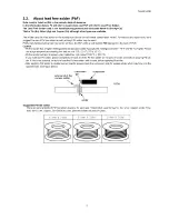
2.2.  About lead free solder (PbF)--------------------------------5

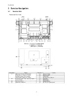
3 Service Navigation------------------------------------------------- 6

3.1.  Service  H int------------------------------------------------------ 6

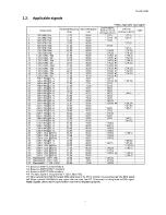
3.2.  Applicable signals--------------------------------------------- 7

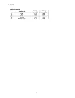
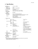
4 S pecifications------------------------------------------------------- 9
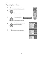
5 Operating  Instructions------------------------------------------ 10
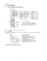
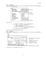
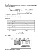
6 Service M ode-------------------------------------------------------12

6.1.  CAT (Computer Aided Test)  m ode--------------------- 12

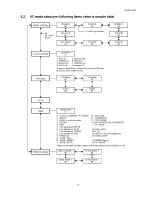
6.2.  IIC  mode  structure  (following  items  value  is

sample data)--------------------------------------------------- 15

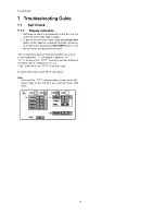
7 Troubleshooting  Guide----------------------------------------- 16

7.1.  Self Check-------------------------------------------------------16

7.2.  No  Power--------------------------------------------------------18

PAGE

7.3.  No  Picture------------------------------------------------------- 18

7.4.  Local  screen failure------------------------------------------ 19

8  Disassembly and Assembly Instructions---------------- 20

8.1.  Removal  of Rear C o ve r---------------------------------- 20

8.2.  Removal  of Slot  B lo ck-------------------------------------20

8.3.  Removal  of DS-Board--------------------------------------20

8.4.  Removal  of HX-Board--------------------------------------20

8.5.  Removal  of A-Board---------------------------------------- 20

8.6.  Removal  of Fan-----------------------------------------------21

8.7.  Removal  of P-Board---------------------------------------- 21

8.8.  Removal  of AC  Inlet Assy---------------------------------21

8.9.  Removal  of H3-Board--------------------------------------22

8.10.  Removal  of SN-Board--------------------------------------22

8.11.  Removal  of SS-Board--------------------------------------22

8.12.  Removal  of S1-Board--------------------------------------23

8.13.  Removal  of C1-Board--------------------------------------23

8.14.  Removal  of C2-Board--------------------------------------23

8.15.  Removal  of  Front  Glass,  V1,  V2-Board  and

Cabinet A ssy-------------------------------------------------- 24

■  

®

Panasonic

©  Panasonic Corporation  2010

Unauthorized  copying  and  distribution  is  a  violation

of law.

Summary of Contents for TH42PH20E

Page 1: ...ctrostatically Sensitive ES Devices 4 2 2 About lead free solder PbF 5 3 Service Navigation 6 3 1 Service Hint 6 3 2 Applicable signals 7 4 Specifications 9 5 Operating Instructions 10 6 Service Mode 12 6 1 CAT Computer Aided Test mode 12 6 2 IIC mode structure following items value is sample data 15 7 Troubleshooting Guide 16 7 1 Self Check 16 7 2 No Power 18 PAGE 7 3 No Picture 18 7 4 Local scre...

Page 2: ...am 12 19 A Board 11 of 16 Schematic Diagram 12 20 A Board 12 of 16 Schematic Diagram 12 21 A Board 13 of 16 Schematic Diagram 12 22 A Board 14 of 16 Schematic Diagram 12 23 A Board 15 of 16 Schematic Diagram 12 24 A Board 16 of 16 Schematic Diagram 12 25 C1 Board Schematic Diagram 12 26 C2 Board Schematic Diagram 12 27 SN Board 1 of 9 Schematic Diagram 12 28 SN Board 2 of 9 Schematic Diagram 12 29...

Page 3: ...ound such as a water pipe as shown in Figure 1 3 Use Leakage Current Tester Simpson 228 or equivalent to measure the potential across the measuring network 4 Check each exposed metallic part and measure the voltage at each point 5 Reserve the AC plug in the AC outlet and repeat each of the above measure 6 The potential at any point TOUGH CURRENT expressed as voltage U1 and U2 does not exceed the f...

Page 4: ...sure of the assembly 3 Use only a grounded tip soldering iron to solder or unsolder ES devices 4 Use only an anti static solder removal device Some solder removal devices not classified as anti static ESD protected can generate electrical charge sufficient to damage ES devices 5 Do not use freon propelled chemicals These can generate electrical charges sufficient to damage ES devices 6 Do not remo...

Page 5: ...oint than standard solder Typically the melting point is 50 70 F 30 40 C higher Please use a high temperature soldering iron and set it to 700 20 F 370 10 C Pb free solder will tend to splash when heated too high about 1100 F or 600 C If you must use Pb solder please completely remove all of the Pb free solder on the pins or solder area before applying Pb sol der If this is not practical be sure t...

Page 6: ...rocessor Sub Field Processor Sync Processor Audio Processor Speaker Out Amplifier C1 Data drive Right C2 Data drive Left S1 Power switch V1 Remote receiver LED G R DS Slot Interface Audio Video Sync Input Switch DC DC Converter V2 Key switch P Power supply SN Scan drive Scan out H3 Speaker terminal SS Sustain drive Sustain out HX PC RS 232C_Input terminal 6 ...

Page 7: ... 59 94 33 54 6 34 24 29 1 024 x 768 50 Hz 39 55 50 00 51 89 30 1 024 x 768 60 Hz 48 36 60 00 65 0 65 0 31 1 024 x 768 70 Hz 56 48 70 07 75 0 32 1 024 x 768 75 Hz 60 02 75 03 78 75 33 1 024 x 768 85 Hz 68 68 85 00 94 5 34 1 066 x 600 60 Hz 37 64 59 94 53 0 53 0 35 1 152 x 864 60 Hz 53 70 60 00 81 62 36 1 152 x 864 75 Hz 67 50 75 00 108 0 37 1 280 x 768 60 Hz 47 70 60 00 80 14 38 1 280 x 960 60 Hz 6...

Page 8: ...TH 42PH20E Video input VIDEO Signal name Horizontal frequency kHz Vertical frequency Hz 1 NTSC 15 73 59 94 2 PAL 15 63 50 00 3 PAL60 15 73 59 94 4 SECAM 15 63 50 00 5 Modified NTSC 15 73 59 94 8 ...

Page 9: ...ACK x 2 DVI D 24 Pin Content Protection AUDIO Stereo mini jack M3 x 1 High Density Mini D sub 15 Pin VBS use HD port AUDIO Stereo mini jack M3 x 1 External Control Terminal D sub 9 Pin Speaker Terminal N2QAYB000535 R6 UM3 Size x 2 TMME289 x 3 1 020 mm x 610 mm x 89 mm approx 25 0 kg net approx 29 0 kg 1 0 Vp p 75 ohm 0 5 Vrms with sync 1 0 Vp p 75 ohm 0 7 Vp p 75 ohm 0 7 Vp p 75 ohm 0 5 Vrms Compl...

Page 10: ...TH 42PH20E 5 Operating Instructions 1 2 3 4 5 Options 3 3 I Slot power I Power On Screen Delay I Clock Display I All Aspect Е Н П П I Auto Setup Е Н Ф Е Б Ш Н I Rotate 10 ...

Page 11: ...imer function Enable Off timer operation Enable Disable Initial Power Mode Normal Sets the power mode of the unit for when the power recovers from failure or after plugging off and in again ID select 0 Set ID number from 0 to 100 Remote ID Off Remote ID function On Off While the Remote ID on standard remote function can not control the unit Serial ID Off Serial ID function On Off Display size Off ...

Page 12: ...button on the remote control 3 times quickly within 2 second this will place the unit into the CAT mode To exit the CAT mode access the ID mode and switch off the main power 6 1 1 IIC mode Select the IIC mode by Up Down button on the remote control at the front page of CAT mode and then press the Action button on the remote control OSD 1024x768 60Hz 16 9 DYNAMIC Hi PANEL W B Adj 4 R DRIVE CO C 04 ...

Page 13: ...6 73 09 31 20 00 00 00 00 00 Factory use New data Original data SOS history Memory data change Address Change by Up Down buttons on the remote control Change by Left Right buttons on the remote control Data 0 0 Change by VOL Up Down buttons on the remote control The data is memorized when switch off the main power To exit the CD mode press the R button on the remote control 6 1 3 SD mode Select th...

Page 14: ...tion number Number Destination Number Destination 0 Japan 16 1 North America 17 2 Europe 18 China 3 Others 19 China Hotel 4 Britain 20 Russia 5 Taiwan 21 Russia Hotel 6 Thailand 22 Hong Kong 7 23 8 Japan Hotel 24 9 North America Hotel 25 10 Europe Hotel 26 11 27 12 Britain Hotel 28 Middle East Hong Kong 13 29 Middle East Hong Kong Hotel 14 Thailand Hotel 30 Australia 15 31 Australia Hotel Default ...

Page 15: ...RIGHTNESS MEASUREMENT 4 RED PATTERN 5 Low Gradation WHITE 6 Low Gradation BLUE 12 2 dot outline 7 Low Gradation GREEN 13 BLUE 8 Low Gradation RED 14 1 WINDOW 2x Brightness 9 RAMP W 15 SCROLL BAR A RAMP RED В RAMP GREEN 17 R G B W Aging С RAMP BLUE 18 0 5 WHITE These are selected by Action button of Remote and press the R button to exit В sub Bright 1 G sub Bright 1 80 W 80 15 ...

Page 16: ...me pressing the OFF TIMER button on the remote control and the screen will show If the IIC ports have been checked and found to be incorrect Or not located then will appear in place of OK 01 in the line of the PTCT means the number of blinks of the Power LED is 1 Reference to 7 1 2 H09 in the line of the PTCT is the error code To exit the CAT mode switch off the main power Note The line of the PTC...

Page 17: ...ction circuit operates and resets to the stand by mode At this time the defective block can be identified by the number of blinks of the Power LED on the front panel of the unit Refer to 7 1 1 Display Indication About blinking LED When blinking four tim es Lighting up Щ Щ Щ ш m i T T t 1st blink 2nd blink 3rd blink 4th blink K I Pause for 3 5 seconds One cycle u 17 ...

Page 18: ... power LED 1 No lit 2 Green is lit then turns red blinking a few seconds later 3 Only red is lit TH 42PH20E No lit OK C h e c k But no AC supplied board 1r NG 1 Check AC power cord or power source Check Fuse F100 F101 F200 PR101 PR900 7 3 No Picture OK Check DS board OK Check A board 18 ...

Page 19: ...TH 42PH20E 7 4 Local screen failure Plasma display may have local area failure on the screen Fig 1 is the possible defect P C B for each local area Fig 1 19 ...

Page 20: ...ble cable from the connector DS1 3 Remove 4 screws and then remove the Slot Block 8 3 Removal of DS Board 1 Remove the Slot Block Refer to Removal of Slot Block 2 Turn over the Slot Block 8 4 Removal of HX Board 1 Disconnect the connector A14 2 Remove 2 Hexagonal Head screws 5 screws and 2 screws O and then remove the HX Board Block 3 Turn over the HX Board Block 4 Disconnect the connector HX1 5 R...

Page 21: ...ew one when Fan exchange 8 7 Removal of P Board 1 Remove the Fan Block Refer to Removal of Fan 2 Disconnect the connectors P2 P6 P7 P9 P11 P25 P35 3 Remove 9 screws and then remove P Board 3 Remove each 1 screw and then remove the Fan from the Fan Fixed Metal 4 Remove each 4 Fan Corner Rubber Cushions from the Fan 5 Reassemble the Fans in reverse order 8 8 Removal of AC Inlet Assy 1 Disconnect the...

Page 22: ...SN14 SN15 SN16 SN17 SN18 3 Disconnect the connectors SN2 SN3 4 Remove the flexible cable from the connector SN20 5 Remove 8 screws and then remove SN Board 8 11 Removal of SS Board 1 Disconnect the connectors A8 A9 A10 A11 A12 A13 A22 A25 A35 2 Remove the flexible cables from the connectors A1 A21 A33 A34 3 Remove 3 screws 4 Remove 2 screws O and then remove the A Board Block 5 Disconnect the conn...

Page 23: ...lock Refer to remove of Fan 2 Remove the Slot Block Refer to remove of Slot Block 3 Remove 5 screws and then remove the Hanger Metal R and the Stand Pole Bracket R 8 Remove the flexible cables from the connectors C10 C11 9 Remove 8 screws and then remove the flexible cables from the connectors CB1 CB2 CB3 CB4 10 Remove 3 screws o and then remove C1 Board 8 14 Removal of C2 Board 1 Remove the Fan B...

Page 24: ...Refer to Removal of S1 Board 3 Disconnect the connectors A11 A22 4 Remove 4 screws and then remove the Handle Fixing Metal L R 5 Remove 3 screws ft Note when fixing fixed Angle upper rear bottom rear Firstly screw on 6 screws 1 2 in order Note when Front Glass is exchanged Paste the Front Glass Sponges in order along each Fixed Angles left and right upper and bottom Note when fixing Handle Fixing ...

Page 25: ... Button Shield 7 Remove 3 hooks and then remove the Power Button and Power Button Spring 8 Disconnect the connector V22 and then remove V2 Board 9 Remove 2 hooks and then remove the 5 Key Button from V2 Board 1 Remove the Front Glass Refer to Removal of Front Glass 2 Remove V1 Board and V2 Board Refer to Removal of V1 Board and V2 Board 3 Remove the LED Panel and Remote Sensor Panel 4 Remove the R...

Page 26: ...e the flexible cable from the connector DS1 5 Remove 4 screws and then remove the Slot Block 6 Disconnect the connectors A8 A9 A10 A11 A12 A13 A22 A25 A35 7 Remove the flexible cables from the connectors C11 C21 SN20 8 Remove 3 screws 9 Remove 2 screws O and then remove the A Board Block 11 Remove 2 screws and then remove the S1 Board Block 12 Remove the flexible cables from the connectors SN11 SN...

Page 27: ...1 Remove 3 screws o r И И ль sJ Handle Fix ML Metal R 3 э Щ 0 0 j n n i m n r mj nq 1 Hanc J Meta 3 ff S i 4 Ц 9 Ш Ф 1 3 l i I p LJJ in ffi 1IT _ v oin t i 5 Щ I Note when fixing Handle Fixing Metal L R Screw on 2 screws 1 firstly 22 Pull the bottom of the Plasma Display Panel forward arrow1 23 Slide the Plasma Display Panel and then remove the Plasma Display Panel arrow2 24 Remove 12 screws and t...

Page 28: ...ring TEST and CONF stage Press 5 button to display the On Screen Display 5 Press VOL button to set to LOW 6 In LOW setting a If no several dead pixel is visible remarkably in white pattern press 3 button to go to CONF stage b If the several dead pixels are visible remarkably in white pattern Set to HIGH by press VOL button Press 3 button to go to CONF stage if the symptom is improved 7 Press OK bu...

Page 29: ...emperature to NORMAL Mid 9 Fix G drive at E0h and adjust B drive and R drive so the highlight window s x y becomes the Color temperature NORMAL Mid in the below table 10 Increase R G B together so the maximum drive value in R G B becomes FCh 11 Set color temperature to WARM Low 12 Set G drive to E0h and adjust B drive and R drive so the highlight window sx ybecome the Color temperature WARM Low sh...

Page 30: ... COOL Hi AO 1180 AO 1181 AO 1182 NORMAL Mid AO 1183 AO 1184 AO 1185 WARM Low AO 1186 AO 1187 AO 1188 Table 4 Drive data addresses PAL nonuse dummy Color temperature R G В COOL Hi AO 1189 A0 118A A0 118B NORMAL Mid A0 118C A0 118D A0 118E WARM Low A0 118F AO 1190 AO 1191 Table 5 Drive data addresses DVI nonuse dummy Color temperature R G В COOL Hi AO 11B6 AO 11B7 AO 11B8 NORMAL Mid AO 11B9 AO 11BA ...

Page 31: ...emperature to NORMAL Mid 9 Fix G drive at E0h and adjust B drive and R drive so the highlight window s x y becomes the Color temperature NORMAL Mid in the below table Increase R G B together so the maximum drive value in R G B becomes FCh Set color temperature to WARM Low 12 Set G drive to E0h and adjust B drive and R drive so the highlight window s x y become the Color temperature WARM Low shown ...

Page 32: ... 11A1 A0 11A2 AO 11A3 Table 8 Drive data addresses YUV1_525ip Color temperature R G В COOL Hi AO 1192 AO 1193 AO 1194 NORMAL Mid AO 1195 AO 1196 AO 1197 WARM Low AO 1198 AO 1199 A0 119A Table 9 Drive data addresses YUV3_625ip Color temperature R G В COOL Hi A0 11A4 A0 11A5 A0 11A6 NORMAL Mid A0 11A7 A0 11A8 A0 11A9 WARM Low AO 11AA A0 11AB AO 11AC 32 ...

Page 33: ...TH 42PH20E 10 Block Diagram 10 1 Main Block Diagram 33 ...

Page 34: ...am D S S L O T IN T E R F A C E TX3 TX9 TX8 TXC TX7 TX2 TX6 TX1 TX5 TX0 TX4 IIC_CONT1 SRQ PLUG DET A_OA OE A_EA EE A_CLK SLOT3 3V SLOT5V SLOT9V SLOT15V LAN14V STB5V J K 3 5 0 9 RS232C J K 3 5 1 3 PC AUDIO IN JK 3 5 1 1 PC IN SLOT1 P6 34 ...

Page 35: ...TH 42PH20E 10 3 Block 2 of 5 Diagram 35 ...

Page 36: ...TH 42PH20E 10 4 Block 3 of 5 Diagram 1 CO MPOSITE Ж 2 4 1 CO MPONENT J K 2 4 2 p v A I D G T A L S G N A L P R O C E S S O R AUDIO IN L R_CV L2 L1 R2 R1 AUDIO INPUT L R_HA L3 R3 AU D IO IN L R_DVI 36 ...

Page 37: ...10 5 Block 4 of 5 Diagram TH 42PH20E PO W ER SUPPLY 37 ...

Page 38: ...TH 42PH20E 10 6 Block 5 of 5 Diagram S N S C A N D R IV E S S S U S T A IN D R IV E 38 ...

Page 39: ...am 11 1 Wiring 1 Clamp position CON No CON No D D A12 Fan A9 P7 No Clamp A10 P6 I I I I I I I I I I I I I I I I I I I A25 P25 No Clamp DS13 A13 H37 A8 HX1 A14 V11 A11 V22 A22 S35 A35 P2 SN2 No Clamp P11 SS11 No Clamp P35 C25 P9 AC lnlet 39 ...

Page 40: ...TH 42PH20E 11 2 Wiring 2 40 ...

Page 41: ...hassis Earth Cold Line Earth Hot 6 Voltage Measurement Voltage is measured by a DC voltmeter Conditions of the measurement are the following Power Source AC220 240V 50 60Hz Receiving Signal Colour Bar signal RF All customer s controls Maximum positions 7 When arrow mark is found connection is easily found from the direction of arrow 8 Indicates the major signal flow Video Audio 9 This schematic di...

Page 42: ...are cold Precautions a Do not touch the hot part or the hot and cold parts at the same time or you may be shocked b Do not short circuit the hot and cold circuits or a fuse may blow and parts may break c Do not connect an instrument such as an oscilloscope to the hot and cold circuits simultaneously or a fuse may blow Connect the earth of instruments to the earth connection of the circuit being me...

Page 43: ...TH 42PH20E 12 2 P Board 1 of 4 Schematic Diagram 42 ...

Page 44: ...TH 42PH20E 12 3 P Board 2 of 4 Schematic Diagram 43 ...

Page 45: ...TH 42PH20E 12 4 P Board 3 of 4 Schematic Diagram 44 ...

Page 46: ... TH 42PH20E 12 5 P Board 4 of 4 Schematic Diagram 10 1 11 1 12 1 13 1 14 1 15 1 16 1 17 1 18 45 ...

Page 47: ...TH 42PH20E 12 6 HX V1 V2 and S1 Board Schematic Diagram A B C D E A H X B O A R D T Z T N P 0 2 1 A E E F 3 4 5 46 ...

Page 48: ...12 7 DS Board 1 of 2 Schematic Diagram D 47 ...

Page 49: ...ТН 42РН20Е А D S BO AR D TZTNP031 С ЕЕ 1 2 IC3000 C0DBAYY00727 SOS BLOCK 6 7 8 9 ...

Page 50: ...TH 42PH20E 12 8 DS Board 2 of 2 Schematic Diagram 10 11 12 13 14 15 16 17 18 48 ...

Page 51: ...TH 42PH20E 12 9 A Board 1 of 16 Schematic Diagram A C D B E F 1 2 3 6 8 9 7 49 ...

Page 52: ...TH 42PH20E 12 10 A Board 2 of 16 Schematic Diagram 10 11 12 13 14 15 16 17 18 50 ...

Page 53: ...TH 42PH20E A 12 11 A Board 3 of 16 Schematic Diagram A B O A R D TZTN P 011A E E 3 16 2 5 13 19 20 21 22 23 24 25 26 27 51 ...

Page 54: ...TH 42PH20E 12 12 A Board 4 of 16 Schematic Diagram 28 29 30 31 32 33 34 35 36 52 ...

Page 55: ...TH 42PH20E 12 13 A Board 5 of 16 and H3 Board Schematic Diagram 37 38 39 40 41 42 43 44 45 53 ...

Page 56: ...TH 42PH20E 12 14 A Board 6 of 16 Schematic Diagram 46 1 47 48 49 1 50 1 51 1 52 53 1 54 54 ...

Page 57: ...TH 42PH20E 12 15 A Board 7 of 16 Schematic Diagram 55 56 57 58 59 60 61 62 63 55 ...

Page 58: ...TH 42PH20E 12 16 A Board 8 of 16 Schematic Diagram S 64 65 66 67 68 69 70 71 72 56 ...

Page 59: ...TH 42PH20E 12 17 A Board 9 of 16 Schematic Diagram 73 74 75 76 77 78 79 80 81 57 ...

Page 60: ...TH 42PH20E 12 18 A Board 10 of 16 Schematic Diagram 58 b 2 ...

Page 61: ...TH 42PH20E A 12 19 A Board 11 of 16 Schematic Diagram A B O A R D TZTN P 011A E E 11 16 A 3 SCX1 VDD18 1 8V 91 92 93 94 95 96 97 98 99 59 ...

Page 62: ... TH 42PH20E 12 20 A Board 12 of 16 Schematic Diagram 100 101 102 103 104 105 106 107 108 60 ...

Page 63: ...e 12 21 А Board 13 of 16 Schematic Diagram SCX1_LVDS 109 110 111 112 113 61 ...

Page 64: ...ТН 42РН20Е 114 115 116 117 ...

Page 65: ...TH 42PH20E 12 22 A Board 14 of 16 Schematic Diagram 118 1 119 1 120 1 121 1 122 1 123 1 124 1 125 1 126 62 ...

Page 66: ...TH 42PH20E 12 23 A Board 15 of 16 Schematic Diagram 63 ...

Page 67: ...matic Diagram Q9900 T P 9 010 9ls Q9901 i i Ц и J Jt i Ц м и Ш il n m 1 s s я J A S 1 ii 1 S i1 2 _ 1 i 1 6 i 2 _ i 1111 S I I a I 1i SH s12iiiiS I 2 f f 1 H i H i I i I П s 5 5 j I t3 TO C2 BOARD C21 136 137 138 139 140 141 142 143 144 64 ...

Page 68: ...12 25 C1 Board Schematic Diagram D A C1 B O A R D T X N C 111 BEK 1 2 3 4 ...

Page 69: ...IC17101 ТН 42РН20Е 6 7 8 9 ...

Page 70: ...TH 42PH20E 12 26 C2 Board Schematic Diagram i 2 3 4 5 6 7 8 9 66 ...

Page 71: ...TH 42PH20E 12 27 SN Board 1 of 9 Schematic Diagram A C D A S N BO AR D T X N S N 11B E K 1 9 IO P BOARD B E F 1 2 3 67 ...

Page 72: ...TH 42PH20E 12 28 SN Board 2 of 9 Schematic Diagram 10 11 12 13 14 15 16 17 18 68 ...

Page 73: ...TH 42PH20E 12 29 SN Board 3 of 9 Schematic Diagram A S N BO AR D T X N S N 11B E K 3 9 19 20 21 22 23 24 25 26 27 69 ...

Page 74: ...TH 42PH20E 12 30 SN Board 4 of 9 Schematic Diagram IC1 471 C0DBEYY00114 I SHUNT REG I IC1 724 C0CBADE00049 IPVSCN 28 29 30 31 32 33 34 35 36 70 ...

Page 75: ...0000018 I PDP SCAN DRIVER Щ Т и r 1 1 r ш r Ш 1 1 E k Isi Is 18 B E E 4 kE l U i l i s I s U i U s s U i i1 i l i l i li a 4 k k k k 4 a 4 т т т ш т т т т ш т т т т ш т т TTTT j4 C 1 a j3 1i C 1 2 0 V S C 4 V 7 exr j I 1 0 П 220 I 220 I Ш 1 S I 1000 I 220 I II 1 1 IC14902 C0HBC0000018 PDP SCAN DRIVER Л r n m 52 53 37 38 39 40 41 42 43 44 45 71 ...

Page 76: ...TH 42PH20E 12 32 SN Board 6 of 9 Schematic Diagram 72 ...

Page 77: ...Л Л Л Л Л Л Л J s J s Л Л Л Л Л Л Л Л Л Л Л Л Л IC14951 C0HBC0000018 I PDP SCAN DRIVER В Д Т I 1 1 7 1 1 8 r n A B 3 7 1 A B 3 7 2 A B 3 7 3 A B 3 7 4 l I I I i f Ц I Ц f I l l I I i f if if if If If If if If if I l if If IfIf If If if If If If Is Is Is Is Is Is Is le Is 1 Is lg Ij lg lg 1 lg lg lg lg lg lg lg lg lg lg lg lg lg lg lg lg lg lg lg lg lg lg lg lg lg lg k lg lg lg lg IC14952 C0HBC0000...

Page 78: ...Ш 1 1 Ш i E г a Is la is s s в Is lg E lg g Ijj I 1 Is Is 1 n S i i L Is S 1 3 i 4 4 5 E s e i ч ч ч ч i isi I т т ш т т ш т т т ш ш ш т п IC14953 C0HBC0000018 I PDP SCAN DRIVER Ш1ПШПГШ1ПР Ш 1 m IC14954 C0HBC0000018 PDP SCAN DRIVER M Ip 1Цr n S П Л С И H П 64ь I I Т 64 65 i i 67 68 69 70 71 72 0 74 ...

Page 79: ...TH 42PH20E 12 35 SN Board 9 of 9 Schematic Diagram 73 74 75 76 77 78 79 80 81 75 ...

Page 80: ...TH 42PH20E 12 36 SS Board 1 of 2 Schematic Diagram A C D A S S BO A R D TX N S S 11B E K 1 2 TO P BOARD P11 B E F 6 5 7 76 ...

Page 81: ...TH 42PH20E 12 37 SS Board 2 of 2 and SS2 Board Schematic Diagram A SS BO A R D T X N S S 11B E K 2 2 PANEL SUSTAIN ELECTRODE PANEL SUSTAIN ELECTRODE 10 11 12 13 14 15 16 17 18 77 ...

Page 82: ...13 Printed Circuit Board 13 1 P Board TH 42PH20E P BOARD FOIL SIDE LSEP1288LMHB 6 5 4 3 2 1 A I B I С I D I E I F I G I H I I I 78 ...

Page 83: ...00 E 1 Q301 E 4 TP700 G 5 IC600 E 1 Q302 E 5 TP900 B 4 IC601 E 2 Q303 E 4 IC602 D 2 Q400 E 3 IC603 D 1 Q401 E 3 IC604 G 1 Q402 E 3 IC700 D 5 Q505 C 1 IC701 C 6 Q600 H 5 IC800 D 2 Q601 C 2 IC901 C 3 Q602 H 5 IC901 C 4 Q609 H 5 IC902 C 3 Q701 D 5 IC903 C 3 Q703 D 5 IC904 C 3 Q705 D 6 Q706 D 6 Q707 D 6 Q708 C 6 Q710 D 5 Q711 D 5 Q712 C 5 Q713 C 5 Q714 D 6 Q715 C 5 Q800 B 2 Q801 C 2 Q804 B 3 Q900 B 3 ...

Page 84: ...ТН 42РН20Е Parts Location P BOARD COMPONENT SIDE 1 C TRANSISTOR VOLUME IC201 D 2 Q103 C 3 R141 D 3 IC400 E 3 Q104 C 3 R923 H 3 Q302 E 5 VR251 F 5 Q303 E 4 Q901 G 4 TEST POINT TP700 C 5 TP900 H 4 ...

Page 85: ...TH 42PH20E P BOARD COMPONENT SIDE LSEP1288LMHB G 6 5 4 3 2 1 E F H 80 ...

Page 86: ... 2 HX Board HX BOARD FOIL SIDE TZTNP021AEE A в С D ...

Page 87: ...ТН 42РН20Е HX BOARD COMPONENT SIDE TZTNP021AEE J9 Л V IHX1I 15 TNPA5110 OR D E R NO C R N O 3D D 0 Pb FJ J 4 J1 J6 J8 5 J K 5 1 1 1 1 5 0 9 JK509 J2 J K 5 1 3 _ Ц r 1 I F I G I H 81 ...

Page 88: ...L SIDE TNPA5163 V2 B0ARD C0MP0NENT SIDE TNPA5163 V1 B0ARD F0IL SIDE TNPA5162 V1 B0ARD C0MP0NENT SIDE TNPA5162 S1 B0ARD F0IL SIDE TNPA5164 TNPA51 64 о с е S E E R E V E R S E F O R X I O R D E R N O S1 BOARD COMPONENT SIDE TNPA5164 A I В I С I D I Ё 82 ...

Page 89: ...L SIDE TNPA5111 H3 B0ARD C0MP0NENT SIDE TNPA5111 1 11 1 1 3 H37 1 h Ш L8501 p y y i g f T N P A 5 1 1 fi5 fH b A A J L8502 T7r7B SEE REVERSE FOR ORDER NO Щ D8501 08503 Ц Ц E H D8S02 D 8 S E H СРОЭ 4 ORDER N O JK 8500 3 8 ...

Page 90: ...TH 42PH20E 13 4 DS Board 6 5 4 A I В I С I D I E I F I G I H I I I 83 ...

Page 91: ...TH 42PH20E 6 5 4 DS BOARD COMPONENT SIDE TZTNP031CEE 84 ...

Page 92: ...TH 42PH20E 13 5 6 5 4 3 2 1 A Board A BOARD FOIL SIDE TZTNP011AEE Ш 85 ...

Page 93: ...TH 42PH20E 86 ...

Page 94: ...13 6 C1 Board TH 42PH20E C1 BOARD FOIL SIDE TXNC111BEK C1 BOARD COMPONENT SIDE TXNC111BEK 6 5 4 3 87 ...

Page 95: ...13 7 C2 Board TH 42PH20E C2 BOARD FOIL SIDE TXNC211BEK C2 BOARD COMPONENT SIDE TXNC211BEK 171 О ф I I I J E l 5 li o n h t ic 1 iz a 2 i G 6 5 4 3 2 1 E F H 88 ...

Page 96: ...13 8 SN Board 6 5 ...

Page 97: ...ТН 42РН20Е ...

Page 98: ...TH 42PH20E А I В I C I D I E I F I G I H I I I 90 ...

Page 99: ...13 9 SS Board 6 5 SS BOARD FOIL SIDE TXNSS11BEK C R N o 16 рь 7 TNPA5072 T SS Q 1 1 i x 1 i 13 XX I X X X 13 1 П Х Х Х Х 1 I 1 A В С D ...

Page 100: ...ТН 42РН20Е 1 I F I G I H 91 ...

Page 101: ...TH 42PH20E 6 5 4 SS BOARD COMPONENT SIDE TXNSS11BEK A I B I C I D I E I F I G I H I I 92 ...

Page 102: ...le for a specific period of time The retention period of availability is dependant on the type of assembly and in accordance with the laws governing part and product retention After the end of this period the assembly will no longer be available Abbreviation of part name and description 1 Resistor 2 Capacitor Example Example ERD25TJ104 С ЮОКОНМ J 1 4W ECKF1H103ZF С 0 01UF Z 50V Type Allowance Type...

Page 103: ... C603 ECJ1VB1H103K C 0 001UF K 50V 1 C607 ECJ1VB1H103K C 0 001UF K 50V 1 Safety Ref No Part No Part Name Description Pcs Remarks A PCB LSEP1288LMHB CIRCUIT BOARD P 1 RTL A PCB TNPA5111 CIRCUIT BOARD H3 1 RTL A PCB TNPA5162 CIRCUIT BOARD V1 1 RTL A PCB TNPA5163 CIRCUIT BOARD V2 1 RTL A PCB TNPA5164 CIRCUIT BOARD S1 1 RTL A PCB TXNC111BEK CIRCUIT BOARD C1 1 RTL PA VCCZ A PCB TXNC211BEK CIRCUIT BOARD...

Page 104: ...V 1 C2304 F1K1E106A136 C 10UF Z 25V 1 C2305 F1J1E105A231 C 1 UF 25V 1 C2306 F1G1H102A730 C 1000UF 50V 1 C2308 F1K1E106A136 C 10UF Z 25V 1 Safety Ref No Part No Part Name Description Pcs Remarks C2309 F1J1E105A231 C 1 UF 25V 1 C2310 F1G1H102A730 C 1000UF 50V 1 C2311 ECJ1VB1A105K C 1UF Z 10V 1 C2312 F1G1C104A116 C 0 10UF K 16V 1 C2313 F1J1E105A231 C 1 UF 25V 1 C2314 F1H1H104A970 C 0 1UF K 50V 1 C231...

Page 105: ...145 C 0 01UF K 16V 1 C3006 F1H1H103A970 C 0 001UF K 50V 1 C3010 F2H1E470A007 E 47UF 25V 1 C3011 F1H1H103A975 C 0 001UF K 50V 1 C3013 F1H1C104A143 C 0 1UF K 16V 1 C3017 F1K1E106A136 C 10UF Z 25V 1 C3018 F1H1E104A129 C 0 1UF 25V 1 C3020 F1H1C104A143 C 0 1UF K 16V 1 C3021 F1K1E106A136 C 10UF Z 25V 1 C3022 F1K1E106A136 C 10UF Z 25V 1 C3023 F1H1C104A144 C 0 1UF K 16V 1 C3024 F1H1E104A129 C 0 1UF 25V 1 ...

Page 106: ...254 EEEHB1C471P C 470PF J 16V 1 C3255 EEEHB1C471P C 470PF J 16V 1 C3256 EEEHB1C471P C 470PF J 16V 1 C3258 F1G1C104A116 C 0 10UF K 16V 1 Safety Ref No Part No Part Name Description Pcs Remarks C3259 F1G1C104A116 C 0 10UF K 16V 1 C3261 F1K1C106A126 C 10UF 16V 1 C3262 F1G1C104A116 C 0 10UF K 16V 1 C3263 F1J0J106A004 C 0 010UF K 16V 1 C3264 F1G1C103A116 C 0 010UF K 16V 1 C3266 ECJ1VB1A105K C 1UF Z 10V...

Page 107: ...A116 C 0 10UF K 16V 1 C4206 F1G1C104A116 C 0 10UF K 16V 1 C4207 F1G1C104A116 C 0 10UF K 16V 1 C4208 F1G1C104A116 C 0 10UF K 16V 1 Safety Ref No Part No Part Name Description Pcs Remarks C4209 F1G1C104A116 C 0 10UF K 16V 1 C4210 F1G1C104A116 C 0 10UF K 16V 1 C4211 F1J0J106A004 C 0 010UF K 16V 1 C4212 F1J0J106A004 C 0 010UF K 16V 1 C4213 F1G1C104A116 C 0 10UF K 16V 1 C4214 F1G1C104A116 C 0 10UF K 16...

Page 108: ...6 C 0 10UF K 16V 1 C4508 F1G1C104A116 C 0 10UF K 16V 1 C4510 F1G1C104A116 C 0 10UF K 16V 1 C4512 F1G1C104A116 C 0 10UF K 16V 1 C4514 F1J0J106A004 C 0 010UF K 16V 1 Safety Ref No Part No Part Name Description Pcs Remarks C4515 F1G1C104A116 C 0 10UF K 16V 1 C4517 F1G1C104A116 C 0 10UF K 16V 1 C4519 F1G1C104A116 C 0 10UF K 16V 1 C4521 F1G1C104A116 C 0 10UF K 16V 1 C4523 F1G1C104A116 C 0 10UF K 16V 1 ...

Page 109: ... Pcs Remarks C4631 F1G1C104A116 C 0 10UF K 16V 1 C4632 F1G1C104A116 C 0 10UF K 16V 1 C4638 F1G1C104A116 C 0 10UF K 16V 1 C4639 F1G1C104A116 C 0 10UF K 16V 1 C4651 F1J0J106A004 C 0 010UF K 16V 1 C4652 F1G1C104A116 C 0 10UF K 16V 1 C4653 F1G1C104A116 C 0 10UF K 16V 1 C4654 F1J0J106A004 C 0 010UF K 16V 1 C4655 F1G1C104A116 C 0 10UF K 16V 1 C4656 F1G1H120A731 C 12UF 50V 1 C4657 F1G1H180A731 C 18UF 50V...

Page 110: ...1 C9312 F1J1A106A087 C 0 010UF K 10V 1 C9313 F1G1C104A116 C 0 10UF K 16V 1 C9314 F1J1A106A087 C 0 010UF K 10V 1 Safety Ref No Part No Part Name Description Pcs Remarks C9315 F1G1C104A116 C 0 10UF K 16V 1 C9316 F1J1A106A087 C 0 010UF K 10V 1 C9319 F1G1C104A116 C 0 10UF K 16V 1 C9322 F1G1C104A116 C 0 10UF K 16V 1 C9323 F1G1C104A116 C 0 10UF K 16V 1 C9325 F1G1C104A116 C 0 10UF K 16V 1 C9327 F1G1C104A...

Page 111: ... 6 3V 1 C16023 F1E2J821A002 C 82PF 600V 1 Safety Ref No Part No Part Name Description Pcs Remarks C16101 F1L2J1020001 C 1000UF K 6 3V 1 C16102 F1L2J562A022 C 5600UF K 6 3V 1 C16103 F1H1E470A130 C 47UF K 25V 1 C16104 F1H1E470A130 C 47UF K 25V 1 C16105 F1E2J221A002 C 22PF 600V 1 PAVCCZ C16106 F1E2J221A002 C 22PF 600V 1 PAVCCZ C16131 F1K1E475A134 C 4 7UF Z 25V 1 C16133 F1K1E475A134 C 4 7UF Z 25V 1 C1...

Page 112: ...UF 100V 1 C17111 F1L2A334A031 E 3300UF 100V 1 C17112 F1L2A334A031 E 3300UF 100V 1 C17113 F1H1C104A143 C 0 1UF K 16V 1 Safety Ref No Part No Part Name Description Pcs Remarks C17208 ECJ1VB1A105K C 0 01UF Z 50V 1 C17209 ECJ1VB1A105K C 0 01UF Z 50V 1 C17210 F1H1C104A143 C 0 1UF K 16V 1 C17211 F1L2A334A031 E 3300UF 100V 1 C17212 F1L2A334A031 E 3300UF 100V 1 C17214 F1H1C104A143 C 0 1UF K 16V 1 C17215 F...

Page 113: ...J056M0L ZENER DIODE 1 D4165 DZ2J056M0L ZENER DIODE 1 D4171 B0ECKM000048 DIODE 1 D4172 B0ECKM000048 DIODE 1 D4371 DZ2J056M0L ZENER DIODE 1 D4372 DZ2J056M0L ZENER DIODE 1 Safety Ref No Part No Part Name Description Pcs Remarks D4374 DZ2J056M0L ZENER DIODE 1 D4663 MA152K DIODE 1 D4664 MA152K DIODE 1 D4665 MA152K DIODE 1 D4701 DZ2J033M0L ZENER DIODE 1 D4703 B0JCCE000008 DIODE 1 D4801 B0BC3R700004 ZENE...

Page 114: ...5V 1 FL3007 F1J1E104A148 C 0 10UF Z 25V 1 FL3008 F1J1E104A148 C 0 10UF Z 25V 1 FL3201 J0HABB000004 LC FILTER 1 FL3202 J0HABB000004 LC FILTER 1 FL3203 J0HABB000004 LC FILTER 1 FL3204 J0MAB0000175 LC FILTER 1 FL3510 TAXA0024 LC FILTER 1 FL3511 TAXA0024 LC FILTER 1 Safety Ref No Part No Part Name Description Pcs Remarks FL3512 TAXA0024 LC FILTER 1 FL3513 TAXA0024 LC FILTER 1 FL3514 TAXA0024 LC FILTER...

Page 115: ...ERJ6GEY0R00V M 0 OHM J 1 10W 1 JA10 ERJ6GEY0R00V M 0 OHM J 1 10W 1 JA11 ERJ6GEY0R00V M 0 OHM J 1 10W 1 JA12 ERJ6GEY0R00V M 0 OHM J 1 10W 1 JA13 ERJ6GEY0R00V M 0 OHM J 1 10W 1 JK2301 K4AC02B00043 EARTH SPRING 1 PAVCCZ JK2401 K2HA4YYB0012 JACK 1 PAVCCZ JK2402 K2HC1YYB0049 JACK 1 JK3201 K1QBB4AB0012 CONNECTOR 1 PAVCCZ JK3509 K1FA109B0062 CONNECTOR 1 JK3511 K1FB115BA020 CONNECTOR 1 JK3513 K2HC1YYB0049...

Page 116: ...6103 G0ZZ00002183 PEAKING COIL 1 L16303 G0C471MA0049 PEAKING COIL 1 PAVCCZ L16401 G0C1R5K00004 PEAKING COIL 1 PAVCCZ L16411 G0C1R5K00004 PEAKING COIL 1 PAVCCZ L16472 G0ZZ00002183 PEAKING COIL 1 L16698 G0C681MA0065 PEAKING COIL 1 L16851 G0ZZ00002183 PEAKING COIL 1 P2 K1KA02A00676 2P CONNECTOR 1 P6 K1KA11AA0082 11P CONNECTOR 1 P7 K1KA14AA0082 14P CONNECTOR 1 P9 K1KA02A00720 2P CONNECTOR 1 Safety Ref...

Page 117: ...3 DSC200100L TRANSISTOR 1 Q9004 DSC200100L TRANSISTOR 1 Q9800 DSC200100L TRANSISTOR 1 Q9802 DSC200100L TRANSISTOR 1 Safety Ref No Part No Part Name Description Pcs Remarks Q9900 DSC200100L TRANSISTOR 1 Q9901 DSC200100L TRANSISTOR 1 Q16001 B1JBEN000002 TRANSISTOR 1 PAVCCZ Q16002 B1JBEN000002 TRANSISTOR 1 PAVCCZ Q16021 B1JBEN000002 TRANSISTOR 1 PAVCCZ Q16022 B1JBEN000002 TRANSISTOR 1 PAVCCZ Q16101 B...

Page 118: ...5JA033 M1 22MOHM J 0 5 W 1 R300 D0GZ181JA020 M 180 OHM J 0 5W 1 R301 D0GZ181JA020 M 180 OHM J 0 5W 1 Safety Ref No Part No Part Name Description Pcs Remarks R302 ERJ8GEYJ220V M 22 OHM J 1 8W 1 R303 ERJ8GEYJ220V M 22 OHM J 1 8W 1 R304 ERX12SJ1R0 M 0 1 OHM J 1 2W 1 R305 ERX12SJ1R0 M 0 1 OHM J 1 2W 1 R400 ERJ6GEYJ222V M 2 2K OHM J 1 10W 1 R401 ERJ6GEYJ203 M 20KOHM J 1 10W 1 R403 ERJ6GEYJ302V M 3KOHM ...

Page 119: ...GEYJ100V M 10 OHM J 1 10W 1 R730 ERJ8GEYJ472V M 4 7KOHM J 1 8W 1 R731 ERJ6GEYJ4R7 M 4 7 OHM J 1 10W 1 R732 ERJ6ENF1802 M 18KOHM 1 10W 1 Safety Ref No Part No Part Name Description Pcs Remarks R733 ERJ6GEYJ4R7 M 4 7 OHM J 1 10W 1 R734 ERJ6GEYJ101V M 100 OHM J 1 10W 1 R736 ERJ6GEYJ101V M 100 OHM J 1 10W 1 R739 ERJ6ENF3901 M 3 9KOHM 1 10W 1 R740 ERJ3GEYJ331 M 330 OHM J 1 16W 1 R741 ERJ6ENF6201 M 6 2K...

Page 120: ...1 2W 1 R923 EVMAASA00B23 CONTROL 2KOHMB 1 R924 ERJ8GEYJ243 M 24KOHM J 1 8W 1 R926 ERJ6ENF2003 M 200KOHM 1 10W 1 Safety Ref No Part No Part Name Description Pcs Remarks R927 ERJ6ENF2003 M 200KOHM 1 10W 1 R928 ERJ6ENF2202 M 2 2KOHM 1 10W 1 R933 ERJ8GEYJ101V M 100 OHM J 1 8W 1 R941 D0XGR10J0003 M 0 100HM J 5W 1 R942 ERJ6GEYJ222V M 2 2K OHM J 1 10W 1 R943 ERJ6GEYJ223 M 22KOHM J 1 10W 1 R944 ERJ6ENF100...

Page 121: ... 100 OHM J 0 063W 1 R2429 D0GA333JA015 M 33KOHM J 0 063W 1 R2430 D0GA473JA015 M 47KOHM J 0 063W 1 Safety Ref No Part No Part Name Description Pcs Remarks R2431 D0GA101JA015 M 100 OHM J 0 063W 1 R2432 D0GB102JA041 M 1KOHM J 1 10W 1 R2433 D0GA101JA015 M 100 OHM J 0 063W 1 R2435 D0GA184JA015 M 180KOHM J 0 063W 1 R2436 D0GA101JA015 M 100 OHM J 0 063W 1 R2437 D0GA333JA015 M 33KOHM J 0 063W 1 R2438 D0GA...

Page 122: ...D0GB563JA041 M 56KOHM J 1 10W 1 Safety Ref No Part No Part Name Description Pcs Remarks R3109 D0GB473JA057 M 47KOHM J 1 10W 1 R3110 ERJ3GEYJ223 M 22KOHM J 1 16W 1 R3111 D0GB103JA057 M 10K OHM J 1 10W 1 R3112 D0GB104JA041 M 100KOHM J 1 10W 1 R3113 D0GB753JA041 M 75KOHM J 1 10W 1 PAVCCZ R3114 D0GB393JA041 M 39KOHM J 1 10W 1 R3122 D0GBR00Z0002 M 0 OHM J 1 10W 1 R3123 D0GBR00Z0002 M 0 OHM J 1 10W 1 R3...

Page 123: ... 063W 1 R3294 D0GA333JA015 M 33KOHM J 0 063W 1 R3295 ERJ3GEYJ101 M 100 OHM J 1 16W 1 Safety Ref No Part No Part Name Description Pcs Remarks R3296 D0GB102JA041 M 1KOHM J 1 10W 1 R3400 ERJ6GEYJ103V M 10K OHM J 1 10W 1 R3508 ERJ6GEYJ472V M 4 7K OHM J 1 10W 1 R3509 ERJ6GEYJ472V M 4 7K OHM J 1 10W 1 R3510 ERJ6GEYJ101V M 100 OHM J 1 10W 1 R3511 ERJ6GEYJ101V M 100 OHM J 1 10W 1 R3529 ERJ6GEYJ184 M 180KO...

Page 124: ...15 M 33 OHM J 0 063W 1 R4106 D0GA473JA015 M 47KOHM J 0 063W 1 R4107 D0GA473JA015 M 47KOHM J 0 063W 1 R4108 D0GA473JA015 M 47KOHM J 0 063W 1 Safety Ref No Part No Part Name Description Pcs Remarks R4109 D0GA473JA015 M 47KOHM J 0 063W 1 R4111 ERJ2GEJ103 M 10KOHM J 0 063W 1 R4112 D0GA473JA015 M 47KOHM J 0 063W 1 R4121 D0GA472JA015 M 4 7KOHM J 0 063W 1 R4122 D0GA472JA015 M 4 7KOHM J 0 063W 1 R4123 D0G...

Page 125: ...0GA101JA015 M 100 OHM J 0 063W 1 R4308 D0GA101JA015 M 100 OHM J 0 063W 1 R4312 D0GA101JA015 M 100 OHM J 0 063W 1 R4313 D0GA101JA015 M 100 OHM J 0 063W 1 R4314 D0GA101JA015 M 100 OHM J 0 063W 1 Safety Ref No Part No Part Name Description Pcs Remarks R4315 D0GA101JA015 M 100 OHM J 0 063W 1 R4316 D0GAR00Z0001 C 0 OHM 0 063W 1 R4321 ERJ2GEJ103 M 10KOHM J 0 063W 1 R4322 ERJ2GEJ103 M 10KOHM J 0 063W 1 R...

Page 126: ... D0GA561JA015 M 560OHM J 0 063W 1 PAVCCZ R4452 ERJ3GEYJ221 M 220 OHM J 1 16W 1 R4454 ERJ3GEYJ101 M 100 OHM J 1 16W 1 Safety Ref No Part No Part Name Description Pcs Remarks R4455 D1BB3300A055 M 330 OHM 1 10W 1 R4456 D1BB1270A055 M 127 OHM 1 10W 1 PAVCCZ R4457 D1BB4300A055 M 430 OHM 1 10W 1 R4458 ERJ3GEYJ101 M 100 OHM J 1 16W 1 R4459 D0GB102JA041 M 1KOHM J 1 10W 1 R4463 D1BA3161A014 M3 16KOHM 0 063...

Page 127: ...R4705 D0GA393JA015 M 39KOHM J 0 063W 1 R4706 ERJ2GEJ103 M 10KOHM J 0 063W 1 R4707 D0GA101JA015 M 100 OHM J 0 063W 1 Safety Ref No Part No Part Name Description Pcs Remarks R4708 ERJ2GEJ103 M 10KOHM J 0 063W 1 R4709 D0GA101JA015 M 100 OHM J 0 063W 1 R4710 ERJ2GEJ102X M 1KOHM J 0 063W 1 R4711 D0GA123JA015 M 12K OHM J 0 063W 1 R4712 D0GA101JA015 M 100 OHM J 0 063W 1 R4713 ERJ2GEJ103 M 10KOHM J 0 063W...

Page 128: ...GEJ103 M 10KOHM J 0 063W 1 R4829 ERJ2GEJ103 M 10KOHM J 0 063W 1 Safety Ref No Part No Part Name Description Pcs Remarks R4831 ERJ2GEJ103 M 10KOHM J 0 063W 1 R4834 EXB38VR000V RESISTOR ARRAY 1 R4835 EXB38VR000V RESISTOR ARRAY 1 R4836 EXB38VR000V RESISTOR ARRAY 1 R4838 D0GA222JA015 M 2 2KOHM J 0 063W 1 R4839 D0GA101JA015 M 100 OHM J 0 063W 1 R4840 D0GA101JA015 M 100 OHM J 0 063W 1 R4841 D0GA101JA015...

Page 129: ...3 D0GB103JA057 M 10K OHM J 1 10W 1 R4994 D0GB103JA057 M 10K OHM J 1 10W 1 R9070 ERJ2GEJ103 M 10KOHM J 0 063W 1 Safety Ref No Part No Part Name Description Pcs Remarks R9072 ERJ2GEJ103 M 10KOHM J 0 063W 1 R9104 EXB38V101JV RESISTOR ARRAY 1 R9105 ERJ2GEJ220 M 22 OHM J 0 063W 1 R9107 D0GA332JA015 M 3 3KOHM J 0 063W 1 R9111 D0GAR00Z0001 C 0 OHM 0 063W 1 R9119 EXB38V470J RESISTOR ARRAY 1 R9121 ERJ2GEJ1...

Page 130: ...R9609 EXB38V470J RESISTOR ARRAY 1 R9610 EXB38V470J RESISTOR ARRAY 1 R9611 EXB38V470J RESISTOR ARRAY 1 R9868 ERJ2GEJ104 M100KOHM J 0 063W 1 Safety Ref No Part No Part Name Description Pcs Remarks R9871 ERJ2GEJ103 M 10KOHM J 0 063W 1 R9872 D1BB3301A055 M 3 3KOHM 1 10W 1 R9873 D1BB1002A055 M 10KOHM 1 10W 1 R9874 D1BB2702A055 M 27KOHM 1 10W 1 R9875 D1BB2002A055 M 20KOHM 1 10W 1 R9877 D1BB4302A055 M 43...

Page 131: ...V M 330KOHM F 0 33W 1 R16290 ERJT08J334V M 330KOHM F 0 33W 1 R16307 ERJ6RBD623 M 62KOHM J 1 10W 1 R16309 ERG1FJS333D M 33KOHM J 1W 1 R16318 ERJ6RBD563 M 56KOHM J 1 10W 1 Safety Ref No Part No Part Name Description Pcs Remarks R16319 ERJ6RBD242 M 2 4KOHM J 1 10W 1 R16320 ERJ14YJ683 M 68KOHM 1 2W 1 R16330 D0GB102JA041 M 1KOHM J 1 10W 1 R16332 D0GB474JA041 M 470KOHM J 1 10W 1 R16334 ERJ3GEYJ472 M 4 7...

Page 132: ...OHM J 1 10W 1 R16663 ERJ3RBD6981 M6 98K OHM 1 13W 1 PAVCCZ R16664 ERJT08J102V M 1KOHM J 0 33W 1 R16665 ERJT06J330V M 33 OHM F 0 25W 1 R16666 D1BB2202A087 M 22KOHM 1 10W 1 Safety Ref No Part No Part Name Description Pcs Remarks R16674 ERJT08J102V M 1KOHM J 0 33W 1 R16675 ERJ3GEYJ472 M 4 7KOHM J 1 16W 1 R16679 D1BB1002A087 M 10KOHM 1 10W 1 R16680 D1BB1002A087 M 10KOHM 1 10W 1 R16681 ERJT06J100V M 10...

Page 133: ...37 D0GB184JA041 M 180KOHM J 1 10W 1 R16938 D0GB184JA041 M 180KOHM J 1 10W 1 R17101 ERJT08J151V M150 OHM F 0 33W 1 R17112 ERJT14J1R0U C1 0 OHM J 1 4W 1 R17116 ERJT14J1R0U C1 0 OHM J 1 4W 1 R17118 ERJT14J1R0U C1 0 OHM J 1 4W 1 R17120 ERJT14J1R0U C1 0 OHM J 1 4W 1 R17124 D0GB470JA041 M 47 OHM J 1 10W 1 R17125 EXB38V470J RESISTOR ARRAY 1 R17126 D0GB681JA041 M 680 OHM J 1 10W 1 R17127 EXB38V681J RESIST...

Page 134: ...00242 3P CONNECTOR 1 VR251 EVMAASA0 0B33 CONTROL 3KOHMB 1 X600 H2B400400021 CRYSTAL 1 X2351 H0J245500089 CRYSTAL 1 X3120 H0J327200114 CRYSTAL 1 X4001 H0J286500023 CRYSTAL 1 X4401 H1C2705B0038 CRYSTAL 1 PAVCCZ X4501 H0J360500017 CRYSTAL 1 X4502 H0J200500076 CRYSTAL 1 X9000 H2C1005A0041 CRYSTAL 1 X9300 H0J200500076 CRYSTAL 1 Z1 K4CZ01000027 AV TERMINAL 1 Z2 K4CZ01000027 AV TERMINAL 1 Z3 K4CZ01000027...

Page 135: ...Model No TH 42PH20E Important Safety Notice Note All parts except parts mentioned PAVCCZ in the Remarks column are supplied by AVC CSPC Parts mentioned PAVCCZ are supplied by PAVCCZ ...

Page 136: ...Model No TH 42PH20E Exploded View ...

Page 137: ...Model No TH 42PH20E Cabinet part location ...

Page 138: ...Model No TH 42PH20E Fan part location 21 ...

Page 139: ...Model No TH 42PH20E Flat cable ...

Page 140: ...Model No TH 42PH20E Packing and Accessories 1 ...

Page 141: ...Model No TH 42PH20E Packing 2 ...

Page 142: ...VER HANDLE 2 17 TMKG5 56 SPONGE FRONT GLASS UPPER BOTTOM 2 18 TMKG5 57 SPONGE FRONT GLASS LEFT RIGHT 2 19 TMKG6 69 FAN SPONGE 1 TMM23417 CLAMPER 2 TMME031 SPACER 2 TMME0 61 CLAMPER 1 TMME2 61 CLAMPER 1 20 TMME2 89 CLAMPER 3 TMME2 91 EDGE SADDLE 1 TMME2 92 CLAMPER 6 TMME3 05 CLAMPER 1 TMME332 CLAMPER 17 TMME35 6 CLAMPER 3 21 TMMJ0 82 SPONGE FAN CORNER 4 22 TMMX16 9 AC CODE CLAMPER B 2 23 TMMX181 AC...

Page 143: ...CABLE C10 C20 1 35 TSXM0 72 1 CABLE DS1 A1 1 36 TSXM081 CABLE A21 SN20 1 37 TSXM082 CABLE A33 C11 1 38 TSXM083 CABLE A34 C21 1 A 39 TTUA23 88 REAR COVER 1 PAVCCZ 40 TUXA3 63 HANGER FIXING METAL L 1 41 TUXA3 65 HANGER FIXING METAL R 1 42 TUXA3 67 HANGER METAL L 1 A 43 TXAJS011CEE AC INLET ASSY 1 PAVCCZ A 44 TXFKY011AEJ CABINET ASSY 1 45 TXFUX0 91AEJ HANGER ASSY R 1 TXJSPR1AEJ SPEAKER LEAD A8 H37 1 ...

Reviews: