background image

Service Manual

LCD Television 

TX-LR24E3


  GLP26 Chassis 


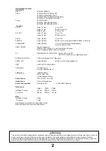
Specifications


 Power 

Source:


220-240V AC, 50 Hz 


Rated Power Consumption: 

46W  


Stand-by Power Consumption:   

0.3W (Without monitor out recording)


9.0W (With monitor out recording) 


 Aerial 

Impedance:

 75

 unbalanced, Coaxial Type 


Receiving System:


DVB-T     Digital  terrestrial  services (MPEG2 and MPEG4-AVC

(H.264)


DVB-C


Digital cable services (MPEG2 and MPEG4-AVC

(H.264) 


PAL-D/K, 


SECAM 

D/K 


PAL-525/60 (AV only) 


M.NTSC 

(AV 

only) 


NTSC (AV only)


Receiving Chanels:


VHF R1-R2                         


VHF R6-R12                       


VHF 

R3-R5 


UHF 

E21-E69 


Aerial - Rear:


VHF/UHF


Operating Conditions: 

Temperature:    0°C 

 35°C 


Humidity: 

  20%  

 80% RH (non condensing)  


©   Panasonic  Corporation 2011.


Unauthorized copying


and 

distribution is a violation of law. 

ORDER No. ITD1106017CE 


Summary of Contents for TX-LR24E3

Page 1: ...pe Receiving System DVB T Digital terrestrial services MPEG2 and MPEG4 AVC H 264 DVB C Digital cable services MPEG2 and MPEG4 AVC H 264 PAL D K SECAM D K PAL 525 60 AV only M NTSC AV only NTSC AV only Receiving Chanels VHF R1 R2 VHF R6 R12 VHF R3 R5 UHF E21 E69 Aerial Rear VHF UHF Operating Conditions Temperature 0 C 35 C Humidity 20 80 RH non condensing Panasonic Corporation 2011 Unauthorized cop...

Page 2: ...V rms 1k high impedance USB USB 2 0 DC 5V Max 500mA CARD SLOT SD CARD slot x1 Common Interface slot x1 LCD screen L5EDDYY00205 1920 x 1080 16 9 Visible Diagonal 610mm Audio Output 10W 2 x 5W 10 THD Headphones 3 5mm 8 Impedance Accessories supplied Remote Control 2 x R6 UM3 Batteries Dimensions Height Width Depth Including TV stand 415mm 595mm 187mm TV set only 380mm 595mm 60mm Mass Including TV st...

Page 3: ...ORMATION 10 REPLACEMENT OF ICS 10 MODEL AND KEYS 10 SETTING INSPECTION 11 SELF CHECK 12 HOTEL MODE 17 DATA COPY BY SD CARD 18 DATA COPY FROM TV SET TO SD CARD 19 DATA COPY FROM SD CARD TO TV SET 20 OPTION BYTES DESCRIPTION 21 ADJUSTMENT METHOD 22 WIRING DIAGRAM 23 BLOCK DIAGRAM 1 OF 2 24 PARTS LOCATION 26 REPLACEMENT PARTS LIST NOTE 28 REPLACEMENT PARTS LIST 29 SCHEMATIC DIAGRAMS 37 A BOARD 1 OF 1...

Page 4: ...d metallic part and measure the voltage at each point 5 Reserve the AC plug in the AC outlet and repeat each of the above measure 6 The potential at any point TOUCH CURRENT expressed as voltage U1 and U2 does not exceed the following values For a c U1 35 V peak and U2 0 35 V peak For d c U1 1 0 V Note The limit value of U2 0 35 V peak for a c and U1 1 0 V for d c correspond to the values 0 7 mA pe...

Page 5: ...d can generate electrical charge sufficient to damage ES devices 5 Do not use freon propelled chemicals These can generate electrical charges sufficient to damage ES devices 6 Do not remove a replacement ES device from its protective package until immediately before you are ready to install it Most replacement ES devices are packaged with leads electrically shorted together by conductive foam alum...

Page 6: ... a higher melting point than standard solder Typically the melting point is 50 70 F 30 40 C higher Please use a high temperature soldering iron and set it to 700 20 F 370 10 C Pb free solder will tend to splash when heated too high about 1100 F or 600 C If you must use Pb solder please completely remove all of the Pb free solder on the pins or solder area before applying Pb solder If this is not p...

Page 7: ...00 66 67 Macintosh 16 832 624 49 73 74 55 Macintosh 21 1 152 870 68 68 75 06 Applicable input signal for PC is basically compatible to HDMI standard timing Signal name Horizontal frequency kHz Vertical frequency Hz 640 480 60 Hz 31 47 60 00 750 720 60p 45 00 60 00 1 125 1 080 60p 67 50 60 00 Note Signals other than above may not be displayed properly The above signals are reformatted for optimal v...

Page 8: ...ackcover Lay the main unit face down see Fig 5 Remove the 3 fixing screws and the pedestal assembly see Fig 6 Remove the 13 fixing screws and the backcover see Fig 7 SCREWS XYN4 F12FJK 3pcs Fig 6 Fig 5 Fig 7 SCREWS XTV3 12JFJK 13pcs 8 ...

Page 9: ... A03 KA10 WIRE A12 SPK WIRE A09 P850 WIRE LVDS WIRE P850 P800 P851 P851 PANEL WIRE Board Name Function A Board AV Terminal HDMI Digital Audio Out SD Card CI slot PC USB TV tuner Peaks_sLD2 AV Switch Speaker out EEPROM Flash Memory DDR SDRAM KA Board Remote Receiver Power and Timer LED C A T S P Board Main Input Power Supply Key Control Power Switch P BOARD KA BOARD A BOARD 9 ...

Page 10: ...ure of models Replacement of ICs When sLD2 IC IC8000 is replaced EEPROM IC8902 should be also replaced with new one the same time When EEPROM IC8902 is replaced sLD2 IC IC8000 is not necessary to be replaced the same time After the replacement of IC SELF CHECK should be done to generate the final KEY data How to SELF CHECK While pressing VOLUME button on the main unit press the STATUS button on th...

Page 11: ...V SUB1 8V TP4801 1 82V 1 89V SUB3 3V TP4800 TP8615 3 20V 3 46V SUB5V TP4802 4 77V 5 25V SUB9V TP5005 8 57V 9 50V Check both testpoints Connect DC 2 5V to TV_SUB_ON P850 connector pin 7 TP850 Connect AC 230V to P800 connector pin1 2 GND connection point connector P850 pin 2 6 P board Description Test point Normal Active STBY Pasive STBY 24V TP852 21 6V 26 4V 5V 15 7V TP853 14 9V 16 5V 5V 5 8VS TP85...

Page 12: ...UNER A Board STBY IC8000 Peaks sLD2 A Board MEM1 IC8901 STM EEPROM A Board MEM2 IC8902 EEPROM PEAKS sLD2 A Board AVSW IC3001 AUDIO VIDEO SWITCH A Board If the CCU ports have been checked and found to be incorrect or not located then will appear in place of O K TX LR24E3 24FHD Panasonic 2011LCD Self Check Complete TUN O K STBY O K MEM1 O K MEM2 O K AVSW O K PEAKS SOFT 1 007 PEAKS EEP 01 02 0004 LSI...

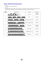
Page 13: ...stand by mode At this time the defective block can be identified by number of blinking of the Power LED on the front panel of the unit Blinking times Blinking timing Contents Check point 1 BL_SOS A BOARD P BOARD 3 SOS A BOARD 4 SUB12V_SENSE_SOS A BOARD 7 SUB3 3V_SENSE_SOS A BOARD 9 SOUND_SOS A BOARD P BOARD 12 BE sLD2 SOS A BOARD 13 EMERGENCY _SOS A BOARD 14 IROM_SOS A BOARD No Light Light 13 ...

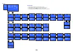
Page 14: ... this chassis The following setting and adjustment can be adjusted by remote control in Service Menu How to enter SERVICE While pressing v button on the TV unit press on the remote control for 3 times within 2 seconds Note To exit from Service mode press the exit button on remote control 0 14 ...

Page 15: ...N SELECT 3 4 SUB SELECT 5 6 BIT SELECT 9 PICTURE MENU SELECT VOL ADJUST OK WRITE 00000100 OPTION DYNAMIC OPT 2 1 2 MAIN SELECT 3 4 SUB SELECT 5 6 BIT SELECT 9 PICTURE MENU SELECT VOL ADJUST OK WRITE 11101110 OPTION DYNAMIC OPT 3 1 2 MAIN SELECT 3 4 SUB SELECT 5 6 BIT SELECT 9 PICTURE MENU SELECT VOL ADJUST OK WRITE 00000001 SRV TOOL DYNAMIC 1 2 MAIN SELECT 9 PICTURE MENU SELECT OK ENTER 00 1 2 3 4...

Page 16: ...will be cleared by Self check indication and forced to factory shipment setting Power ON Time On Off Note To display TIME COUNT menu highlight position then press MUTE for 3sec Time Cumulative power on time indicated hour minute by decimal On Off Number of On Off switching by decimal Note This indication will not be cleared by either of the self checks or any other command Exit Disconnect the AC c...

Page 17: ...able PC selectable with VGA option Initial POS Select programme number Selection Off 0 to 99 Off give priority to the last memory Initial VOL Level Adjust the volume when each time power is switched on Selection Range Off 0 to 100 Off give priority to the last memory Maximum VOL Level Adjust maximum volume Range 0 to 100 Button Lock Select local key conditions Selection Off SETUP MENU ALL Off alto...

Page 18: ...ocument A new file is created by default New Text Document txt 3 Right click the new text document that you just created and select rename and then change the name and extension of the file to the following file name a or b and press ENTER File name a For Board replacement boardreplace pwd b For Hotel hotel pwd Note Please make only one file to prevent the operation error No any other file should ...

Page 19: ...er the completion of copying to SD card remove SD card from TV set 5 Turn off the TV set Note Following new folder will be created in SD card for data from TV set a For Board replacement user_setup b For Hotel hotel Data copy Board replacement or Hotel Input Password 2770 or 4850 Performing Completion Performing Data Copy Board replacement Input password Data Copy Board replacement Input password ...

Page 20: ... will be deleted after copying Limited one copy b For Hotel Data will not be deleted and can be used for other TVs 5 Turn off the TV set Note 1 Depending on the failure of boards function of Data for board replacement does not work 2 This function can be effective among the same model numbers Input Password Performing Input Password 2771 or 4851 Performing Completion Performing Data Copy Board rep...

Page 21: ...NICAM scan ON 1 OFF 0 b5 NICAM BG enable 5 5MHz ON 1 OFF 0 b6 NICAM I enable 6 0MHz ON 1 OFF 0 b7 NICAM DK enable 6 5MHz ON 1 OFF 0 OPTION3 b0 NICAM priority ON 1 OFF 0 b1 Starhub scan enable Singapore ON 1 OFF 0 b3 A2 DK2 enable ON 1 OFF 0 b4 Inhibition of countermeasure for SIF signal drop ON 1 OFF 0 b5 Get onid from physical CH CHINA ON 1 OFF 0 b6 SSU search enable for HOTEL model ON 1 OFF 0 b7...

Page 22: ... the letter of Contrast will change from red to black White Balance adjustment 1 Procedure basically performs checking using the production software and make automatic adjustment using external computer 2 It adjusts in the mode of Colour balance Normal Viewing Mode Dynamic Normal Highlight x 0 290 0 010 y 0 297 0 010 Normal Lowlight x 0 306 0 010 y 0 313 0 010 Let the panel standfor more than 3 ho...

Page 23: ...A BOARD AV scart JK1003 HDMI2 JK1021 TU4801 A12 SP A03 KA BOARD KA10 A09 D3050 DIGITAL AUDIO OUT LCD PANEL P BOARD P850 MAIN IN A15 HP JK1052 P800 P851 USB JK1030 JK1001A YUV V IN AUDIO I O RCA PC Side Terminals TUNER Rear Terminals Wiring Diagram KEY CONTROL KEY 23 ...

Page 24: ... 17 STB_RST 28 IC8200 DDR3 SUB1 5V IC8201 DDR3 SUB1 5V DDR3 I F A09 5 8VS P15V STB5 8V 1 3 4 5 7 8 TO P850 10 11 BL_SOS BL_ON PWM_A_OUT 12 13 LCD_TV_SUB_ON LCD_TV_SUB_ON 8 PEAKSRST BL_SOS BL_ON IECOUT IECOUT IC8902 EEPROM sLD2 SUB3 3V I2C V1 EEP_WP A12 IC4900 C1AB00003457 AUDIO AMP 8 9 10 11 1 2 3 4 19 20 35 36 SP_L SP_R 32 33 34 28 29 30 25 26 27 21 22 23 L L R R L L R R V5 V6 Y3 Y2 AUDIO PWM P15...

Page 25: ...T800 1 ZCD 1 PC801 Photo coupler 2 FB 12 3 IS Q802 PC800 Photo coupler PC802 Photo coupler IC850 DC DC converter 12 Vin 1 SW 5 8VS 11 EN Q852 P850 3 4 TO A09 P15V P15V P15V 11 12 13 BL_SOS BL_ON PWM D856 PA850 P851 3 2 1 BL_SOS BL_ON PWM 7 6 TO PANEL 13 D854 PA851 Q853 24V 24V SW850 R859 Q850 7 LCD_TV_SUB_ON Q855 STB5 8V 8 5 1 10 KEY1 IC851 KEY CONTROL SW851 SW852 SW854 SW855 SW853 KEY1 25 ...

Page 26: ...Parts Location 12 14 6 8 15 7 2 16 NOTE The numbers on the exploded view below refer to the exploded view section of the Replacement Parts List 26 ...

Page 27: ...Parts Location NOTE The numbers on the exploded view below refer to the exploded view section of the Replacement Parts List 5 11 4 17 13 3 1 4 10 18 9 27 ...

Page 28: ...Replacement Parts List Note NOTE All parts except parts mentioned PAVCCZ are supplied by AVC CSPC Parts mentioned PAVCCZ are supplied by PAVCCZ 28 ...

Page 29: ...801 TOP CUSHION SET TPD0E1180 BOTTOM CUSHION SET TPD0E2185 SET COVER TPE0E4057 POLYBAG PEDESTAL TPE0E9007 PLASTIC BAG TPE0E9011 SCREW XSB3 4FJ SCREW XTV3 12JFJK SCREW XTW3 10TFJ SCREW XYN3 J8FJ SCREW XYN4 F12FJK INSTRUCTION BOOKS KAZAKHSTAN TQB0E21189 RUSSIAN TQB0E2118L UKRAINIAN TQB0E2118Y I C s PWM CONTROLLER IC800 C0DBBYY00029 DC DC CONVERTER IC850 C0DBAYY00922 REGULATOR IC851 C0DBZMC00006 AUDI...

Page 30: ...39 COIL L850 G0C270MA0049 COIL L851 EXCELSA35 COIL L852 J0JHC0000077 COIL L2001 J0JYC0000065 COIL L2750 J0JYC0000065 COIL L2751 J0JYC0000065 COIL L2752 J0JYC0000065 COIL L2754 J0JYC0000065 COIL L3002 G1C100MA0072 CHIP INDUCTOR L3102 J0JYC0000331 CHIP INDUCTOR L3103 J0JYC0000331 COIL L3108 J0JCC0000287 CHIP INDUCTOR L3111 J0JYC0000331 CHIP INDUCTOR L3112 J0JYC0000331 CHIP INDUCTOR L3113 J0JYC000033...

Page 31: ...154JA052 125W 5 150K Ω SMD R883 D0GD473JA036 125W 5 47K Ω SMD R884 D0GD103JA036 125W 5 10K Ω SMD R885 D0GD101JA036 125W 5 100 Ω SMD R886 D0GD101JA036 125W 5 100 Ω SMD R887 D0GD101JA036 125W 5 100 Ω SMD R888 D0GD102JA036 125W 5 1K Ω SMD R889 D0GD683JA036 125W 5 68K Ω SMD R890 D0GD103JA036 125W 5 10K Ω METAL R892 ERG2SJ680P 2W 5 68 Ω SMD R898 D0GD473JA052 125W 5 47K Ω SMD R899 D0GD473JA052 125W 5 47...

Page 32: ...7K Ω SMD R4000 D0GDR00J0004 125W 5 0 Ω SMD R4024 D0GA103JA015 063W 5 10K Ω SMD R4089 D0GA103JA015 063W 5 10K Ω SMD R4090 D0GAR00J0005 063W 5 0 Ω SMD R4095 D0GAR00J0005 063W 5 0 Ω SMD R4096 D0GAR00J0005 063W 5 0 Ω SMD R4524 D0GA103JA015 063W 5 10K Ω SMD R4560 D0GA273JA023 063W 5 27K Ω SMD R4602 D0GA103JA015 063W 5 10K Ω SMD R4607 D0GA220JA023 063W 5 22 Ω SMD R4608 D0GA103JA015 063W 5 10K Ω SMD R460...

Page 33: ...4 D0GA680JA023 063W 5 68 Ω SMD R8405 D0GA680JA023 063W 5 68 Ω SMD R8408 EXB2HV680J 063W 5 68 Ω SMD R8409 EXB28V680JX 031W 5 68 Ω SMD R8410 EXB2HV680J 063W 5 68 Ω SMD R8411 EXB2HV680J 063W 5 68 Ω SMD R8418 D0GA103JA015 063W 5 10K Ω SMD R8421 EXB2HV101J 063W 5 100 Ω SMD R8424 D0GA223JA023 063W 5 22K Ω SMD R8425 D0GA223JA023 063W 5 22K Ω SMD R8426 D0GA473JA015 063W 5 47K Ω SMD R8427 D0GA473JA015 063W...

Page 34: ... S M CAP C864 F1J1E105A231 25V 1µF ELECT C865 F2A1E1020019 25V 1000µF S M CAP C866 F1K1E106A136 25V 10µF S M CAP C867 F1J1H105A449 50V 1000nF S M CAP C869 F1J1H102A721 50V 1nF S M CAP C870 F1J1E1050003 25V 1000nF S M CAP C872 F1K1E106A136 25V 10µF S M CAP C873 F1J1H223A623 50V 22nF S M CAP C874 F1J1H101A709 50V 100pF S M CAP C875 F1J1H103A807 50V 10nF S M CAP C876 F1J1H472A702 50V 4 7nF S M CAP C8...

Page 35: ...F1G1H1020008 50V 1nF S M CAP C4937 F1G1H1020008 50V 1nF S M CAP C4938 F1K1E106A136 25V 10µF S M CAP C4939 F1K1E106A136 25V 10µF S M CAP C4970 F1J1A106A087 10V 10µF S M CAP C4971 F1J1A106A087 10V 10µF ELECT C4972 F2H1A101A040 10V 100µF ELECT C4973 F2H1A101A040 10V 100µF S M CAP C4977 F1K1E106A136 25V 10µF S M CAP C4978 F1K1E106A136 25V 10µF S M CAP C5000 ECJ1VB1A105K 10V 1000nF ELECT C5001 F2H0J101...

Page 36: ... 25V 10nF S M CAP C8702 F1J1A106A043 10V 10µF S M CAP C8703 F1J1A106A043 10V 10µF S M CAP C8705 F1G1E1030005 25V 10nF S M CAP C8707 F1G1E1030005 25V 10nF S M CAP C8708 F1J1A106A043 10V 10µF S M CAP C8709 F1J1A106A043 10V 10µF S M CAP C8710 F1J1A106A043 10V 10µF S M CAP C8711 F1G1C223A081 16V 22nF S M CAP C8712 F1G1H272A571 50V 2 7nF S M CAP C8714 F1J1A475A087 10V 4 7µF S M CAP C8715 F1J1A106A087 1...

Page 37: ... change without notice REMARKS a Do not touch the hot part or the hot and cold parts at the same time as you are liable to a shock hazard b Do not short circuit the hot and cold circuits as electrical components may be damaged c Do not connect an instrument such as an oscilloscope to the hot and cold circuits simultaneously as this may cause fuse failure Connect the earth of the instruments to the...

Page 38: ...0910 EXB28V472JX R0943 68 R0931 22 R0935 68 R0948 68 R0911 47k R0904 2 7k R0912 0 R0913 0 R80903 2 7k R0939 68 R0901 2 7k R0949 68 R0945 1k R0930 22 R0925 22 R0951 47k R0922 22 R0936 68 R0906 2 7k R0938 68 R0932 22 R0902 2 7k R0924 22 R0941 68 R0940 68 R0907 2 7k R0923 22 R0962 68 R0963 68 R0964 68 R0965 68 R0966 68 R0967 68 R0900 2 7k R0933 22 R0952 1k R0934 68 R0944 100 R0937 68 R0942 68 R0905 2...

Page 39: ...P_RX1M1 asdf P_STM5VDET2 P_STMDDCSDA1 5VDET0 asdf P_RX0CM asdf P_STMCEC0 DDC_SDA_1 asdf 5VDET1 asdf P_STMDDCSDA0 DDC_SDA_0 asdf P_STM5VDET1 DDC_SCL_0 asdf P_RX0P1 asdf P_RX0CP asdf P_PORT07 P_STMDDCSDA2 P_STMCECPUL P_STM5VDET0 P_RX1P2 asdf P_RX1M2 asdf P_RX1P0 asdf DDC_SCL_1 asdf P_RX1P1 asdf P_RX1CP asdf P_RX1CM asdf HPD1 asdf P_STM_CEC0 asdf P_STM_CEC0 asdf P_RX1M0 asdf ARC1 asdf P_RX0P0 asdf P_...

Page 40: ...TP4802 TP4903 TP4800 TP4901 TP4900 TP4902 TP4801 TP4803 P_PWM0RN P_PWM0LP P_PWM0LN P_NSHUTDOWN AMP_STBY AV_R P_PWM0RP HP_MUTE EXT_MUTE EXT_MUTE P_HP1_L AV_L P_MUTEB P_HP1_R DEMOD_IFAGC HP_ROUT P_A_MUTE HP_LOUT AC_TV1_V P_LIN1_RP P_LIN1_LP SOUND_SOSDET IFD OUT2 MONITOROUT_MUTE IFD OUT1 TER_TUNER_SDA TER_TUNER_SCL P_PORT35 P_SIFINN P_SIFINP Q4974 DSC2001S0L Q4972 B1AAFB000002 Q4971 B1AAFB000002 Q497...

Page 41: ... E_AV2_GREEN 11P A_AV2C_Y__TERMINAL E_AV2_Q LINK 10P _TERMINAL AVSW_R044PIN_CVBS Y COUT3 HP_ROUT AVSW_R052PIN_L3OUT AVSW_R067PIN_R5IN AVSW_R097PIN_PRIN1 AVSW_R005PIN_CVBSIN4 AVSW_R015PIN_B2 CIN2 SIDE_HP_R_TERMINAL E_AV2_LOUT _3PIN _TERMINAL AVSW_R070PIN_L7IN AVSW_R100PIN_VDIN AVSW_R095PIN_CYIN1 AVSW_R023PIN_CVBSIN2 SIDE_HP_L_TERMINAL AVSW_R061PIN_R2IN AVSW_R013PIN_G2 YIN2 AVSW_R043PIN_SAGCVBSOUT3 ...

Page 42: ...N2 B3 AVSW_R059PIN_R1IN AVSW_R043PIN_SAGCVBSOUT3 AVSW_R093PIN_PBIN1 AVSW_R079PIN_CVBSIN6 AVSW_R091PIN_PRIN2 R3 AVSW_R005PIN_CVBSIN4 AVSW_R062PIN_L3IN AVSW_R018PIN_TDET2 AVSW_R020PIN_S2DET1 AVSW_R061PIN_R2IN AVSW_R063PIN_R3IN AVSW_R081PIN_CVBSIN5 AVSW_R017PIN_CVBSIN1 Y1 AVSW_R068PIN_L6IN AVSW_R037PIN_SAGCVBSOUT4 AVSW_R027PIN_FBOUT TDET10 AVSW_R002PIN_HDIN AVSW_R070PIN_L7IN AVSW_R001PIN_GIN AVSW_R07...

Page 43: ..._AGW PORT35 FE_XRST SDRAM_CHK1 TCON3 PORT127 PORT33 SD_LED_ON IRQ PORT31 AVDD_ENB PORT122 PORT34 SD REC_LED_ON PORT64 PORT32 LCD_EEP_WP XIRQ11 PORT145 PORT37 SD_PWR_ON XIRQ6 PORT36 EEPROM_WP PEAKS SLD2 TRCD5 PORT67 TRCD4 XIRQ8 TRCD3 TRCD2 PEAKS SLD2 TRCD1 PORT37 TRCD6 TRCD7 DMD TRCD0 TRCST PEAKS SLD2 TRCCLK PORT143 BEEXTRG NU PORT63 REV_DAC_ENB PORT73 NOUSE PORT64 PANEL_TEST_ON PORT42 I2C debug mo...

Page 44: ...J8411 VJ8403 VJ8400 VJUMP1005 S VJ8412 VJ8413 VJ8406 VJUMP3216 P VJ8409 VJUMP2012 P VJ8410 TP8402 TP8404 TP8400 TP8403 TP8406 TP8405 CI_DATAOUTA4 P_HSDOUT5 P_RMCO CI_CD1 CI_INPACK CI_PKTSTOUTA CI_DATAOUTA2 P_HSDOUT7 CI_DATAOUTA0 P_HSDOUT3 P_HSDOUT2 CI_DATAOUTA7 CI_TSCLKIN P_HSBCLKOUT P_HSSYNCOUT CI_DATAOUTA3 P_HSDOUT1 CI_ENOUTA P_HSDOUT4 P_HSVALOUT CI_WAIT P_HSDOUT0 CI_DATAOUTA6 CI_IREQ CI_DATAOUT...

Page 45: ..._WAKEUP P_TCON6 P_TCON4 TD1P_CN P_TB2P P_TCON1 P_TD2P TD2N_CN P_TCON5 P_STMTIME3 P_TCON7 P_TC1N P_TCLK1P P_TF1P P_TE1P TC2P_CN TD2P_CN TA1P_CN TD1N_CN TE1P_CN TC1N_CN TB1P_CN TE1N_CN TD1P_CN TA1N_CN TCLK2N_CN TB2P_CN TCLK1N_CN TA2P_CN TA2N_CN TC1P_CN TE2N_CN TCLK2P_CN TE2P_CN TD2N_CN TB1N_CN TB2N_CN TC2N_CN TCLK1P_CN P_WUC P_PORT32 P_PORT12 P_LVDSRREF P_PORT32 R4090 0 R4024 10k R8306 24k R4095 0 R...

Page 46: ...B5V 5 8VS SUB5V STB3 3V SUB3 3V VJ8701 VJ5101 VJ5008 VJ5150 VJ5002 VJ5003 VJ5001 VJ5007 VJ5004 VJ5005 VJ5006 TP5002 TP5300 TP5005 TP5004 TP5003 PWM_A_IN SOUND_SOSDET SW_OFF_DET PEAKSRST PEAKSRST2 ASIC SUBON SOS_SENSE PWM_POW_ON SOUND_SOS STB_RST TV_SOS P_STMTIME1 AP_OVP_DET EXT_MUTE TV_SOS P_XRSTSTM SOUND_SOS SW_OFF_DET PWM_A_OUT STB_RST PEAKSRST ASIC SUBON AP_OVP_DET HP_MUTE AMP_STBY DCDCEN PEAKS...

Page 47: ...TERMINAL CI_DATAOUTA5 CI_INPACK CI_ENOUTA CI_TSCLKIN E_AV2_GREEN 11P A_AV2C_Y__TERMINAL E_AV2_VIN 20P A_AV3_V__TERMINAL PC_B_TERMINAL E_YPBPR_PB A_AV1C_PB__TERMINAL E_YPBPR_PR A_AV1C_PR__TERMINAL HP_GND E_PC_RIN A_AV1_RIN__TERMINAL E_AV2_BLUE _7PIN _TERMINAL E_PC_LIN A_AV1_LIN__TERMINAL CI_CD2 CI_DATAOUTA6 E_YPBPR_Y A_AV1C_Y__TERMINAL E_AV2_FB 16P _TERMINAL CI_DATAOUTA0 CI_DATAOUTA7 CI_IREQ E_AV2_...

Page 48: ...INV24V STB3 3V DCDCIN VJ8702 TP2016 TP2769 TP2015 TP2771 TP2014 TP2772 TP2775 TP2017 TP2012 TP2002 TP2774 TP2011 TP2773 TP2013 TP2008 TP2019 P_STMTIME0 P_STMTIME4 PWM_A_OUT P_STMADIN0 KEY1 P_STMRMIN P_STMTIME2 P_STMADIN2 LCD_TV_SUB_ON R2018 47k R2019 47k R2012 2 2k R2006 100 R2009 100 R2753 0 R2752 0 R2772 0 100 sht Analog ASIC 700 sht STM P83 KEY1 KEY1 BL_SOS BL_ON STM Port STM Port AI P80 AI_SEN...

Page 49: ... P_PORT00 P_PORT03 P_TMS P_PORT01 P_PORT02 P_TRST P_PORT06 P_TDI AH_EA6 P_ED4 P_ED3 P_ED2 P_ED5 AH_EA3 AH_ED4 P_ED0 P_XNFWE P_ED10 P_ED9 P_NFALE P_ESZ0 P_ED7 P_XIRQ1 P_XNFWP AH_ED1 P_ED15 P_NFCLE AH_ED2 AH_EA1 AH_EA2 AH_ED4 AH_ED1 AH_EA6 AH_EA4 AH_ED7 AH_EA5 AH_ED6 AH_ED3 AH_ED0 AH_EA3 AH_ED5 AH_ERXW AH_EA7 AH_ED3 AH_ED2 AH_EA2 P_XECS0 P_XEWE0 P_ESZ1 P_EA1 P_EA7 STM EEP_SDA STM EEP_SCL PEAKS EEP_S...

Page 50: ...k R8624 56 R8639 10k R8626 56 R8606 4 7k R8642 0 1 6 x 0 8 R8607 4 7k R8625 56 R8627 56 R8628 56 R5609 10k R8640 10k R8636 22 R8641 0 1 0 x 0 5 R8629 56 R864810k C R8672 10k R865010k C C C C C R865310k C C R8671 10k R8673 10k R864910k R865110k R864710k C R8670 10k C R5606 10k TP5601 P_USB0DP_TERMINAL VBUS0 TP5602 P_USB0VBUS C0DBZYY00368 IC5602 R5524N003A TR SE RICOH CO LTD 1 Vin 2 GND 3 EN 4 FLG 5...

Page 51: ...12 IC8000 M21 HS0DIN6 IC8000 M22 HS0DIN3 IC8000 M23 HS0BCLKIN IC8000 M24 PCCD2 IC8000 M25 PCREADY IC8000 M26 PCWAIT IC8000 N1 PORT01 IC8000 N2 PORT03 IC8000 N3 PORT04 IC8000 N4 PORT02 IC8000 N5 PORT07 IC8000 N6 PORT05 IC8000 N9 VSS IC8000 N10 VSS IC8000 N11 VSS IC8000 N12 VSS IC8000 N13 VDD12 IC8000 N14 VDD12 IC8000 N15 VDD12 IC8000 N16 AVDDPLLD2_33 IC8000 N17 VSS IC8000 N18 AVDDAPUSB33_0 IC8000 N...

Page 52: ...10100L C0DBGYY00281 IC5416 XC6204F502PR 1 NC 2 VSS 3 CE 5 VOUT 4 VIN C C5477 1u 10V C IC8702 C0DBAFG00029 S 1172B1J E6T1G 1 VOUT 2 VSS 3 ON OFF 4 NC 5 VSS 6 VIN C8765 10V 1u SUB3 3V C8716 16V 0 1u C5476 1u 10V SUB1 8V STB5 8V R8100 1 3k 1 10W 1 6 x 0 8 AGND1 C8120 22u 4V Q8102 B1MBEDA00027 ECH8666 P TL H S1 G1 S2 G2 D2 D2 D1 D1 PGND1 L8100 G1C4R7MA0416 R8104 820 C8100 6800p 25V AGND1 C8128 22u 4V ...

Page 53: ...F7 DQL1 IC8200 N9 VDD IC8200 T8 A8 IC8200 L1 NC IC8200 M2 BA0 IC8200 K9 CKE IC8200 N8 BA1 IC8200 B3 VSS IC8200 K8 VDD IC8200 J2 VSS IC8200 T7 NC IC8200 N2 A3 IC8200 G2 DQL6 IC8200 M9 VSS IC8200 C8 DQU2 IC8200 F3 DQSL IC8200 R1 VDD IC8200 L9 NC IC8200 D2 VDDQ IC8200 K1 ODT IC8200 E8 VSSQ IC8200 E9 VDDQ IC8200 L8 ZQ IC8200 L3 WE IC8200 G1 VSSQ IC8200 N7 A12 BC IC8200 C3 DQU1 IC8200 F2 DQL2 IC8200 D9...

Page 54: ...50 K1KA16AA0658 B16B PASK LF SN 1 2 3 4 5 6 7 8 9 10 11 12 13 14 15 16 L852 J0JHC0000077 L802 J0JHC0000075 L801 EXCELDR35V L851 EXCELSA35V L803 EXCELSA39V L850 G0C270MA0049 T800 G4DYA0000294 SRW4344EM X03H019 1 2 5 6 7 9 10 12 3 8 11 13 4 F800 K5D312BNA007 02153 15MXBP C C C C C C C C C C C C GND C HGND ZA802 K9ZZ00000424 ZA800 K9ZZ00000424 ZA801 K9ZZ00000424 PC800 B3PBA0000459 PC802 B3PBA0000459 ...

Page 55: ... GC2 TP2807 TP2800 TP2809 TP2808 TP2801 TP2802 TP2804 TP2803 TP2806 RM2800 PNJ4815M01TV 1 2 3 Q2801 DSC200100L Q2802 DSC200100L Q2800 DSC200100L R2807 5 6k R2802 22k R2811 10k R2801 47k R2809 10k R2803 47k R2806 47 R2804 10k R2808 180k R2810 100k 1 R2805 2 26k 1 R2800 953 R2826 0 POWER_LED AI_SENSOR RM_RECEIVER G_LED_ON SUB3 3V REMOTE STBY 3 3 R_LED_ON AI GND ONTIMER_LED_ON TO A03 KA BOARD TNPA537...

Page 56: ...D TNP0EA019 TOP 1 2 3 4 5 A B C D E IC S IC8900 5D IC4900 1B IC5000 4C TRAN S IC5300 1E Q0900 4B IC8000 2C Q4604 3C IC8200 2D Q4971 5A IC8201 3D Q4972 5A IC8404 4D Q4973 5C IC8700 3E Q8100 3D IC8701 2E Q8102 3D IC8702 2A 56 ...

Page 57: ...19 BOTTOM 5 4 3 2 1 A B C D E IC S TRAN S IC3001 3B Q3102 3B IC5416 1E Q3103 3B IC5602 5A Q3104 3A IC8100 3D Q3105 3A IC8401 4D Q4600 2B IC8402 4D Q4750 3B IC8403 5D Q4751 3C IC8706 2C Q4974 5C IC8901 4B IC8902 3C 57 ...

Page 58: ...P BOARD TNP0EP019 TOP 4 3 2 1 A B C D E TRAN S D802 2C Q800 3C D803 2C D805 1B DIODE S D806 1B D800 3A D813 3B D801 2B D816 2C 58 ...

Page 59: ... 2C D808 2C IC850 3D D810 2C IC851 1D D811 2C D812 2C TRAN S D815 2C Q801 1C D818 2C Q802 2C D853 3D Q803 1C D854 1E Q850 2D D855 2D Q851 2D D856 2E Q852 4D D857 4D Q853 1E D858 3D Q854 4D D861 4E Q855 4D D863 4E Q856 4E D864 3E D866 4E DIODE S D867 3E D804 1C 59 ...

Page 60: ...KA BOARD TNPA5378 TOP 1 A 2 IC S RM2800 1A SN2800 1A TRAN S Q2800 2A Q2801 2A Q2802 1A 60 ...

Reviews: