background image

O RDER  NO.  PCZ0904061CE

Plasma Television

Model  No. 

TX-PR37C10

GPH12DE Chassis

A

 WARNING

This service  information  is designed for experienced  repair technicians only and  is not designed for use by the  general  public.

It does not contain warnings or cautions to  advise  non-technical  individuals of potential  dangers  in  attempting to service a product. 
Products powered  by electricity should  be  serviced  or repaired  only by experienced  professional technicians.  Any attempt to  service 

or repair the  product or  products dealt with  in this service  information  by anyone else could  result  in  serious injury or death.

IMPORTANT SAFETY NOTICE

There  are  special  components  used  in  this  equipment which  are  important  for  safety.  These  parts  are  marked  by 

A  

in  the  Schematic 

Diagrams, Circuit Board  Diagrams,  Exploded Views and  Replacement Parts List.  It is essential that these critical parts should be replaced 

with  manufacturer's  specified  parts  to  prevent  shock,  fire  or  other  hazards.  Do  not  modify  the  original  design  without  permission  of 

manufacturer.

Panasonic'

©   Panasonic C orporation  2009.

Unauthorized  copying  and  distribution  is  a  violation 

o f law.

Summary of Contents for TX-PR37C10

Page 1: ... to service or repair the product or products dealt with in this service information by anyone else could result in serious injury or death IMPORTANT SAFETY NOTICE There are special components used in this equipment which are important for safety These parts are marked by A in the Schematic Diagrams Circuit Board Diagrams Exploded Views and Replacement Parts List It is essential that these critica...

Page 2: ...7 11 Schematic Diagram 39 11 1 Schematic Diagram Note 11 2 P Board 11 3 P Board 11 4 P Board 11 5 P Board 11 6 GK K and S Board Schematic Diagram 11 7 A Board 11 8 A Board 11 9 A Board 11 10 A Board A Board 12 A Board 13 A Board 14 A Board 15 A Board 16 A Board 17 A Board 18 A Board 19 A Board 20 A Board A Board 22 A Board 23 A Board 24 A Board 25 A Board 26 A Board 27 A Board 11 11 11 11 11 11 11...

Page 3: ...re 1 3 Use Leakage Current Tester Simpson 228 or equivalent to measure the potential across the measuring network 4 Check each exposed metallic part and measure the voltage at each point 5 Reserve the AC plug in the AC outlet and repeat each of the above measure 6 The potential at any point TOUGH CURRENT expressed as voltage U1 and U2 does not exceed the following values For a c U1 35 V peak and U...

Page 4: ...f the assembly 3 Use only a grounded tip soldering iron to solder or unsolder ES devices 4 Use only an anti static solder removal device Some solder removal devices not classified as anti static ESD protected can generate electrical charge sufficient to damage ES devices 5 Do not use freon propelled chemicals These can generate electrical charges sufficient to damage ES devices 6 Do not remove a r...

Page 5: ...the melting point is 50 70 F 30 40 C higher Please use a high temperature soldering iron and set it to 700 20 F 370 10 C Pb free solder will tend to splash when heated too high about 1100 F or 600 C If you must use Pb solder please completely remove all of the Pb free solder on the pins or solder area before applying Pb sol der If this is not practical be sure to heat the Pb free solder until it m...

Page 6: ...eaker out AV Terminal AV Switch Digital Signal Processor SYSTEM MPU HDMI Switch Peaks lite 2p Format Converter Plasma AI Sub Field Processor C2 Data Driver Lower Left SC Scan Drive SS Sustain Drive SS2 Sustain out Lower SM Scan out Non serviceable SM Board should be exchanged for service K Remote receiver Power LED GK Key Switch S Power Switch 6 ...

Page 7: ...rom HDMI terminal Applicable input signal for PC is basically compatible to HDMI standard timing Signal name Horizontal frequency kHz Vertical frequency Hz 640 x 480 60 Hz 31 47 60 00 750 720 60p 45 00 60 00 1 125 1 080 60p 67 50 60 00 Note Signals other than above may not be displayed properly The above signals are reformatted for optimal viewing on your display PC signal is magnified or compress...

Page 8: ...1 S41 Hyperband VHF R3 R5 UHF E21 E69 Playback of NTSC tape from some PAL Video recorders VCR Playback from M NTSC Video recorders VCR Playback from NTSC Video recorders VCR TV signals may not be received in some areas V H F UHF Temperature Humidity 0 C 35 C 20 80 RH non condensing 21 Pin terminal Audio Video in Audio Video out RGB in Q Link 21 Pin terminal Audio Video in Audio Video out RGB in S ...

Page 9: ...T Model ID 06 STBY EEP 021e3100 STBY ROMCOR 00000040 PDP SOFT RB Cn 000 PDP EEP PDP FPGA PDP PDROM Press 1 Button I Sub Item 1 1 Ia d ju s t i CONTRAST i 0000i YMAX 5 1 1 Key command 1 button Main items Selection in forward direction 2 button Main items Selection in reverse direction 3 button Sub items Selection in forward direction 4 button Sub items Selection in reverse direction RED button All ...

Page 10: ...ALL DRV FC OPTION Panel Type 37HD Factory Boot ROM Preset STBY SET 00 EMERGENCY ON Y С Delay 0 OPT 1 00011100 OPT 2 11101111 ОРТЗ 00000001 AGING RGBW Vertical line All white COUNTER All white All red All green All blue ON OFF Diagonal lamp W Diagonal lamp R Diagonal lamp G Diagonal lamp В 1 WINDOW COLOR BAR A В zone checkerd 4 trio SCROLL BAR 2dot width border Low setup Red Low setup Green Low set...

Page 11: ... left side Last SOS before Last three occurrence before 2nd occurrence after shipment 1st occurrence after shipment This indication will be cleared by Self check indication and forced to factory shipment setting 5 2 3 POWER ON Time On Off Note To display Time On Off menu highlight position then press MUTE for 3sec Time Cumulative power on time indicated hour minute by decimal On Off Number of On O...

Page 12: ...s switched on Selection Off RF AV1 AV2 AV2S AV3 AV3S C OMPONENT HDMI1 HDMI2 Off give priority to a last memory However Euro model is compulsorily set to TV AVnS AVnC only Euro model selectable PC selectable with VGA option Initial POS Select programme number Selection Off 0 to 99 Off give priority to a last memory Initial VOL level Adjust the volume when each time power is switched on Selection Ra...

Page 13: ...e pressing VOLUME button on the main unit press MENU button on the remote con trol for more than 3 seconds 6 1 2 Screen display 6 1 3 Check Point Confirm the following parts if NG was displayed Display Ref No Description P C B ADV IC4510 AD HDMI A Board ADAV IC2106 Sound Processor A Board TUN TU8301 Tuner A Board GENX IC1100 GenX STB MCU A Board MEM1 IC1101 EEPROM GenX A Board MEM2 IC8601 EEPROM P...

Page 14: ...D Flashing timing chart 2 Contents When an abnormality has occurred the unit the protection circuit operates and reset to the stand by mode At this time the defective block can be identified by the number of blinks of the Power LED on the front panel of the unit 14 ...

Page 15: ...6 3 No Power First check point There are following 2 states of No Power indication by power LED 1 No lit 2 Red is lit then turns red blinking a few seconds later See 6 2 15 ...

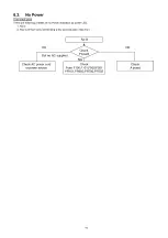
Page 16: ...6 4 No Picture No Picture Check NG 16 ...

Page 17: ...6 5 Local screen failure Plasma display may have local area failure on the screen Fig 1 is the possible defect P C B for each local area Fig 1 17 ...

Page 18: ...ectors P2 P6 P7 P9 P11 P25 P34 and P35 3 Remove the screws x9 and remove the P Board 7 3 Remove the Side terminal cover and Rear terminal cover 1 Remove the claw x1 2 Remove the Side terminal cover 7 4 Remove the Tuner unit 1 Unlock the cable clampers to free the cable 2 Disconnect the connectors A1 A7 A11 A12 and A25 3 Disconnect the flexible cables A20 A31 and A32 4 Remove the screws x2 x1 cz an...

Page 19: ...r A12 See section 7 4 5 Remove the screws x2 and remove the Speaker L Speaker 7 7 Remove the Control button unit 1 Disconnect the connector C14 2 Remove the screws x1 x1 O 3 Remove the Control button unit C1 Board 7 8 Remove the GK Board 1 Remove the Control button unit See section 7 7 2 Remove the screws x2 3 Remove the GK Board MTG metal GK Board MTG metal GK Board Control button 4 Remove the cl...

Page 20: ...3 Disconnect the connectors SC2 and SC3 4 Disconnect the flexible cable SC20 5 Remove the screws x6 and remove the SC Board 1 Remove the Tuner unit See section 7 4 2 Disconnect the bridge connector SS22 SS24 and dis connect the flexible cable SS58 3 Remove the screws x2 and remove the SS2 Board 7 11 Remove the SS2 Board 7 12 Remove the SS Board 1 Remove the Tuner unit See section 7 4 2 Unlock the ...

Page 21: ... x8 4 Disconnect the flexible cables CB1 CB2 CB3 and CB4 5 Disconnect the connector C14 6 Disconnect the flexible cable C10 7 Remove the screws x4 and remove the C1 Board 1 Remove the Tuner unit See section 7 4 2 Remove the Hanger metal L See section 7 13 3 Remove the flexible cables holder fastening screws x8 O 4 Disconnect the flexible cables CB5 CB6 CB7 and CB8 5 Disconnect the flexible cables ...

Page 22: ...t and remove 3 Remove the Rear cover hooks L R 1 Remove the Cabinet assy See section 7 16 2 Remove the S Board shield case 7 17 Remove the S Board 3 Remove the screws x2 and remove the S Board unit 4 Disconnect the connector S1 5 Remove the Power button 6 Remove the screw x1 and remove the S Board 22 ...

Page 23: ...a panel itself without Hanger metals is fragile To avoid the damage to new plasma panel carry a new plasma panel taking hold of the Hanger metals after assembling the Hanger metals and the Stand brackets 1 Place a carton box packed a new plasma panel on the flat surface of the work bench 2 Open a box and without taking a new plasma panel Attach the C1 Board and the C2 Board connect the flexi ble c...

Page 24: ...m the Vad Vad_base but may be measured from the GND GND_base in an unavoidable case 8 1 1 2 Adjustments Adjust driver section voltages referring the panel data on the panel data label Check or adjust the following voltages with the multimeter Name Test Point Voltage Volume Remarks Vsus TPVSUS SS Vsus 2V R737 P Ve TPVE SS Ve 2 5V Fixed Vset TPVSET SC 290V 9V Fixed Vad TPVAD SC 180V 2V VR16600 SC Vs...

Page 25: ...000US Y2 93 6523U dX 10O 000US dY 250 Z28U 1 dX 10 00000kHZ V ______________________________________________________________________________________________________________________J 8 1 3 P C B Printed Circuit Board exchange 8 1 3 1 Caution 1 To remove P C B wait 1 minute after power was off for discharge from electrolysis capacitors 8 1 3 2 Quick adjustment after P C B exchange Adjust the followi...

Page 26: ...8 1 4 Adjustment Volume Location 8 1 5 VR16600 Vad Test Point Location 26 ...

Page 27: ...ow 100 White 2 Goes into service adjustment mode 3 Push a 1 or 2 key and goes into adjustment mode for CONTRAST Adjustment 1 The colour key yellow button of remote control is pushed 2 The OSD character of sub contrast becomes red Inside under automatic adjustment 3 The OSD character of sub contrast returns to black 4 End Ref RF signal modulation spec UK models 80 Other models 90 Note Sub contrast ...

Page 28: ... Inside under automatic adjustment 3 The OSD character of sub contrast returns to black 4 End Steps Another procedure Adjustment of HD system 1 At 1080i 100 Full White or Split colour bar receive component signal as shown below Remarks 100 White 2 Goes into service adjustment mode 3 Push 1 or 2 key and goes into adjustment mode for Contrast Adjustment 1 The colour key yellow button of remote contr...

Page 29: ...al receiver of color analyzer to the highlight window s center and adjust B drive and R drive so x y become the COLOR TEMP COOL in the below table 7 All RGB drive increase so that the maximum drive value of RGB may become FC ALL DRIVE set to FC 8 Set colorbalance to NORMAL using 7 key 9 Fix G CUTOFF B CUTOFF and R CUTOFF at 80 10 Fix G drive at E0 37 inch 42inch D0 50 inch 11 Adjust B DRIVE and R ...

Page 30: ...the signal receiver of color analyzer to the highlight window s center and adjust B drive and R drive so x y become the COLOR TEMP COOL in the below table 7 All RGB drive increase so that the maximum drive value of RGB may become FC ALL DRIVE set to FC 8 Set colorbalance to NORMAL using 7 key 9 Fix G CUTOFF B CUTOFF and R CUTOFF at 80 Fix G drive at E0 37 inch 42inch D0 50 inch Adjust B DRIVE and ...

Page 31: ...9 Block Diagram 9 1 Main Block Diagram 31 ...

Page 32: ...9 2 Block 1 3 Diagram JK8302 SPEAKER L SPEAKER R SD CARD SLOT 32 ...

Page 33: ...9 3 Block 2 3 Diagram RM2501 REMOTE 33 ...

Page 34: ...9 4 Block 3 3 Diagram s s s u s t a i n d r iv e P O W E R S U P P LY s c s c a n d r i v e 34 ...

Page 35: ...gram 10 1 Caution statement Caution Please confirm that all flexible cables are assembled correctly Also make sure that they are locked in the connectors Verify by giving the flexible cables a very slight pull 10 2 Wiring 1 35 ...

Page 36: ...10 3 Wiring 2 36 ...

Page 37: ...щ н ш 10 4 Wiring 3 WIRE No CLAMPER No 1 2 3 4 A11 SPKR 0 0 0 0 A1 K1 0 0 0 0 A12 SPKL 0 IaTT WIRE No CLAMPER No 1 2 3 4 5 6 7 A11 SPKR О О О О О О О A1 K1 О О О 37 f 1 Л ...

Page 38: ...38 ...

Page 39: ...hassis Earth Cold Line Earth Hot 6 Voltage Measurement Voltage is measured by a DC voltmeter Conditions of the measurement are the following Power Source AC220 240V 50 60Hz Receiving Signal Colour Bar signal RF All customer s controls Maximum positions 7 When arrow mark is found connection is easily found from the direction of arrow 8 Indicates the major signal flow Video A u d io s 9 This schemat...

Page 40: ...d Precautions a Do not touch the hot part or the hot and cold parts at the same time or you may be shocked b Do not short circuit the hot and cold circuits or a fuse may blow and parts may break c Do not connect an instrument such as an oscilloscope to the hot and cold circuits simultaneously or a fuse may blow Connect the earth of instruments to the earth connection of the circuit being measured ...

Page 41: ...11 2 P Board 1 4 Schematic Diagram 40 0 ...

Page 42: ... 0 11 3 P Board 2 4 Schematic Diagram TO A BOARD A25 T O P B O A R D 4 4 10 11 12 13 14 15 16 17 18 41 ...

Page 43: ...11 4 P Board 3 4 Schematic Diagram A B C D E A P BOARD LSEP1279BEHB 3 4 F 1 2 3 4 42 ...

Page 44: ... 11 5 P Board 4 4 Schematic Diagram 10 1 11 1 12 1 13 1 14 1 15 1 16 1 17 1 18 43 ...

Page 45: ...11 6 GK К and S Board Schematic Diagram A С F 1 2 3 ...

Page 46: ...S BOARD TXN S1 ETUE ...

Page 47: ...11 7 A Board 1 21 Schematic Diagram A A A BOARD 1 21 IIC REF No 0900 0999 F 3 4 5 45 ...

Page 48: ...11 8 A Board 2 21 Schematic Diagram A A B O A R D 2 21 GenX REF No 1100 1499 10 11 12 13 14 15 16 17 18 SUB3 3V 46 ...

Page 49: ...11 9 A Board 3 21 Schematic Diagram A A BOARD 3 21 ADV REF No 4500 4799 I a d VI IC4510 C1AB00003045 PowerSupply A D V 7496 A D A V4622 19 20 21 22 23 24 25 26 27 47 ...

Page 50: ...11 10 A Board 4 21 Schematic Diagram A A BOARD 4 21 ADV_V REF No 4500 4799 28 29 30 31 32 33 34 35 36 48 ...

Page 51: ...11 11 A Board 5 21 Schematic Diagram 37 38 39 40 ...

Page 52: ...А A BOARD 5 21 ADV_V REF No 4500 4799 41 42 43 44 45 49 ...

Page 53: ...11 12 A Board 6 21 Schematic Diagram TO 6 71 46 47 48 49 50 50 ...

Page 54: ...А A BOARD 6 21 ADV_A REF No 2000 2499 51 52 53 54 ...

Page 55: ...11 13 A Board 7 21 Schematic Diagram 55 56 57 58 59 60 61 62 63 51 ...

Page 56: ...11 14 A Board 8 21 Schematic Diagram TO 7 21 A A BOARD 8 21 A V S W REF No 3000 3399 64 65 66 67 ...

Page 57: ...ТО 9 21 ТО 7 21 68 69 70 71 72 52 ...

Page 58: ...11 15 A Board 9 21 Schematic Diagram A A BOARD 9 21 AVSW REF No 3000 3399 ISUB5V 73 1 74 1 75 1 76 1 77 1 78 1 79 1 80 1 81 53 ...

Page 59: ...11 16 A Board 10 21 Schematic Diagram A A B O A R D 10 21 TUNER REF No 2900 2999 I TUNER5V1 IC2960 82 83 84 85 86 87 88 89 90 54 ...

Page 60: ...11 17 A Board 11 21 Schematic Diagram A A B O A R D 11 21 STB RESET REF No 5400 5499 99 91 92 93 94 95 96 97 98 55 ...

Page 61: ...11 18 A Board 12 21 Schematic Diagram 100 101 102 103 104 105 106 107 108 56 ...

Page 62: ... 0 11 19 A Board 13 21 Schematic Diagram 109 1 110 1 111 1 112 1 113 1 114 1 115 1 116 1 117 57 ...

Page 63: ...11 20 A Board 14 21 Schematic Diagram DO W N LEFT 118 119 120 121 122 123 124 125 126 58 ...

Page 64: ...L 8D R N W E l8r ba1 L8R A 9 l8r a4 L8R A 11 L8R A3 L 8R _ A 2 L8R A0 L8RA6 47 C L8R A 5_______ L8R A 8 V L 8 R S A C LK O 1 3 r 5 iL8AR C L K IC9901 C3ABQY000032 d d r s d r a m 2 2 Q9301 R T i A 32 A A BOARD 15 21 мЧПЧуЧШнЧШуЧШуЧшН5 4 D O W N R IG H T TO C2 BOARD C22 127 128 129 130 131 132 133 134 135 to DDR 59 ...

Page 65: ...11 22 A Board 16 21 Schematic Diagram A A BOARD 16 21 IC5401 C0CBZZE00001 C O M M O N 136 137 138 139 140 141 142 143 SUB9V 15V SUB9V output B 0 B C 0 1 H 0 0 1 F15V 144 60 ...

Page 66: ... E 2 P R O M TO 20 21 TO 1 21 TO 13 21 TO 11 13 21 C N 010 R E M O C O N i SA A Q A e A A BOARD 17 21 Set REF No 2750 2899 t e m p s e n s o r IC1000 C1ZBZ0003775 STB5V FOR FACTORY USE FOR FACTORY USE STB3 3V S R Q P a ne l A prE 2P R O M TO 1 11 21 P a n e l A prE 2P R O M FOR FACTORY USE 153 145 146 147 148 149 150 151 152 61 ...

Page 67: ...11 24 A Board 18 21 Schematic Diagram Peaks Lite2 DDR2 CRNo 8000 8299 Peaks Lite2 162 62 154 155 156 157 158 159 160 161 A A BOARD 18 21 ...

Page 68: ...11 25 A Board 19 21 Schematic Diagram A A BOARD 19 21 DTV CRNo 8300 8999 163 164 165 166 ...

Page 69: ...63 ...

Page 70: ...11 26 A Board 20 21 Schematic Diagram 172 A BOARD 20 21 DTV CRNo 8300 8999 173 174 175 176 177 178 179 180 64 ...

Page 71: ...11 27 A Board 21 21 Schematic Diagram A A BOARD 21 21 DTV 181 182 183 184 185 186 187 188 189 65 ...

Page 72: ...11 28 C1 Board 1 2 Schematic Diagram A B C D E A C1 BOARD TN PA4890 1 2 K 4C D 0 1 0 0 0 0 1 3 K 4 C D 0 1 0 0 0 0 1 3 F ZA 1710 K 4 C D 0 1 0 0 0 0 1 3 K 4 C D 0 H 0 0 0 1 3 1 66 ...

Page 73: ...11 29 C1 Board 2 2 Schematic Diagram A C 10 C2 BOARD 18 10 11 12 13 14 15 16 17 C1 BOARD TN PA4890 2 2 67 ...

Page 74: ...11 30 C2 Board 1 2 Schematic Diagram A C2 BOARD TNPA4891 1 2 TO A BOARD A31 C21 л B 68 ...

Page 75: ...11 31 C2 Board 2 2 Schematic Diagram TO A BOARD A32 10 11 12 13 14 15 16 17 18 69 ...

Page 76: ...11 32 SC Board 1 3 Schematic Diagram в D A SC BOARD TXNSC1 ERUE 1 3 1 2 3 4 ...

Page 77: ...IC16771 C0CBADC00072 70 ...

Page 78: ...11 33 SC Board 2 3 Schematic Diagram 10 11 12 13 14 15 16 17 18 71 ...

Page 79: ...11 34 SC Board 3 3 Schematic Diagram 19 20 21 22 23 24 25 26 27 72 ...

Page 80: ...11 35 SS Board 1 2 Schematic Diagram A B C D E F 3 4 5 73 ...

Page 81: ...11 36 SS Board 2 2 and SS2 Board Schematic Diagram A SS BOARD TXN SS 1E R U E 2 2 PANEL SUSTAIN ELECTRODE 10 11 12 13 14 15 16 17 18 74 ...

Page 82: ...12 Printed Circuit Board 12 1 P Board P BOARD FOIL SIDE LSEP1279BEHB 6 5 4 3 2 1 A I B I C I D I E I F I G I H I I 75 ...

Page 83: ...03 D 2 Q202 D 3 IC300 E 4 Q300 D 3 IC301 E 5 Q301 D 3 IC302 C 2 Q302 D 5 IC303 C 3 Q303 D 4 IC304 C 3 Q304 D 5 IC500 D 2 Q305 D 4 IC502 C 1 Q306 D 5 IC600 D 2 Q307 D 4 IC601 D 3 Q500 D 1 IC602 B 2 Q502 C 2 IC603 B 2 Q503 D 1 IC604 D 2 Q504 C 2 IC700 B 4 Q505 C 2 IC701 B 3 Q506 D 1 IC702 B 3 Q507 C 1 Q600 H 5 Q602 H 5 Q609 I 5 Q610 C 2 Q611 D 3 Q700 A 3 Q701 C 3 Q702 B 3 Q703 C 5 Q704 B 4 Q705 C 3 ...

Page 84: ...D COMPONENT SIDE 1C TRANSISTOR VOLUME IC101 D 4 Q103 C 5 R141 D 4 IC102 D 4 Q104 C 4 R735 H 3 IC201 D 2 Q105 F 4 R737 I 5 IC301 E 4 Q205 F 4 IC502 F 1 Q304 F 5 TEST POINT IC502 F 1 Q404 F 4 TPVDA I 3 IC702 H 3 TPVSUS H 5 76 ...

Page 85: ...P BOARD COMPONENT SIDE LSEP1279BEHB 77 ...

Page 86: ...2 Board SS2 B0ARD FOIL SIDE TNPA4806 SS2 BOARD COMPONENT SIDE TNPA4806 D E R D IP b 7 GK BOARD FOIL SIDE TXNGK1EQUE S BOARD FOIL SIDE TXN S1ETUE S BOARD COMPONENT SIDE TXN S1ETUE GK BOARD COMPONENT SIDE TXNGK1EQUE В 78 ...

Page 87: ...K BOARD FOIL SIDE TXN K1ETUE K BOARD COMPONENT SIDE TXN K1 ETUE ...

Page 88: ...12 3 A Board A BOARD FOIL SIDE A PR37C10 6 5 4 3 2 1 A I B I C I D I E I F I G I H I I 79 ...

Page 89: ...G 2 IC4513 E 4 Q2023 D 3 IC5480 C 5 Q2901 C 2 IC5600 C 5 Q2902 D 2 IC5601 D 5 Q2903 C 1 IC8004 G 4 Q2904 C 3 IC8301 D 2 Q3001 G 2 IC8302 D 2 Q3002 F 2 IC8401 F 6 Q3303 F 2 IC8403 E 5 Q4500 F 3 IC8404 E 5 Q4501 E 3 IC8405 E 5 Q4533 E 4 IC8408 D 5 Q4534 F 4 IC8554 F 5 Q8401 D 6 IC8601 F 6 Q8402 D 6 IC9001 G 6 Q8851 F 4 IC9500 H 6 Q8852 E 4 Q9000 H 5 Q9001 H 5 Q9002 G 6 Q9003 G 1 Q9004 G 6 80 ...

Page 90: ...5470 E 4 Q3005 E 1 IC8001 C 5 Q4514 D 3 IC8002 C 5 Q4515 D 3 IC8003 C 5 Q4516 D 3 IC8409 E 6 Q4517 D 3 IC8410 F 5 Q4519 D 3 IC8411 F 6 Q4520 G 4 IC9003 C 6 Q4535 G 4 IC9004 B 5 Q5480 E 1 IC9303 C 3 Q5565 E 4 IC9805 C 3 Q5600 G 5 IC9806 D 4 Q5601 F 5 IC9807 B 5 Q5602 F 5 IC9808 C 3 Q5603 G 5 IC9900 B 4 Q5606 F 5 IC9901 C 4 Q5607 F 5 Q5608 E 5 Q8200 E 5 Q8850 D 5 Q8853 D 5 Q9301 B 5 Q9302 B 6 Q9807 ...

Page 91: ...A BOARD COMPONENT SIDE A PR37C10 81 ...

Page 92: ...oard 6 C1 BOARD FOIL SIDE TNPA4890 Parts Location C1 BOARD IC IC17101 H 2 IC17102 G 2 IC17103 H 2 IC17104 H 2 И Ш C1 BOARD COMPONENT SIDE TNPA4890 Г г t j j i_ __J 5 4 3 2 1 A I B I C I D I E I F I G I H I I 82 ...

Page 93: ... BOARD FOIL SIDE TNPA4891 Parts Location C2 BOARD IC IC17201 D 2 IC17202 D 2 IC17205 C 2 IC17206 C 1 IC17207 E 2 IC17208 E 2 IC17210 A 2 IC17211 A 2 IC17212 B 2 C2 BOARD COMPONENT SIDE TNPA4891 B G 6 5 4 3 2 1 E F H 83 ...

Page 94: ...12 6 SC Board SC BOARD FOIL SIDE TXNSC1ERUE 6 5 4 3 2 1 A I B I C I D I E I F I G I H I I 84 ...

Page 95: ...TP20 TP21 TP22 TP23 TP24 TP25 TP26 TP27 TP28 TP29 TP30 TP31 TP32 TP33 TP34 TP35 TP36 TP37 TP38 TP39 TP40 A 2 A 2 A 2 A 2 I 2 I 2 1 1 I 2 F 2 F 2 G 1 G 2 F 2 F 2 H 2 H 2 F 2 F 2 I 3 F 2 F 2 H 2 H 2 I 2 F 2 F 2 F 2 F 2 F 2 F 2 F 2 F 2 F 2 F 2 F 2 F 2 F 2 F 2 F 2 TP41 TP42 TP43 TP44 TP51 TP52 TP53 TP59 TP60 TP61 TP62 TP63 TP64 TP65 TP67 TP70 TP73 TP74 TP78 TP79 TP80 TP81 TP90 TP91 TP92 TP93 TP94 TP95...

Page 96: ...5 A 3 TPVAD B 3 IC16563 A 4 Q16676 A 3 TPVSCN B 3 IC16581 E 1 Q16701 B 4 TPVSET H 5 IC16661 B 4 TRANSISTOR Q16702 C 5 TPVSUS I 4 IC16692 C 4 Q16401 G 4 Q16762 E 4 IC16724 B 4 Q16402 F 4 Q16815 B 2 VOLUME IC16725 B 4 Q16421 D 4 Q16816 D 3 IC16771 F 3 Q16422 D 4 Q16817 B 2 VR16600 C 4 IC16773 C 5 Q16441 F 2 Q16818 C 4 VR16601 D 4 IC16784 C 3 Q16442 F 2 Q16874 I 5 IC16786 B 3 Q16451 D 1 Q16875 H 5 IC...

Page 97: ...SC BOARD COMPONENT SIDE TXNSC1ERUE B G 6 5 4 3 2 1 E F H 86 ...

Page 98: ...P62 E 2 Q16021 C 2 TP17 I 3 TP63 E 2 VOLUME Q16022 C 2 TP18 I 3 TP64 E 2 VR16001 G 3 TP24 I 3 TP65 E 2 TP25 E 3 TP66 E 2 TP26 A 2 TP67 E 2 TP27 I 3 TP68 D 2 TP28 G 2 TP69 D 2 TP29 A 3 TP70 D 2 TP30 C 3 TP71 D 2 TP31 C 2 SS BOARD FOIL SIDE TXNSS1ERUE C 0 1 1 C 0 1 2 I C L C 0 P b TNPA4774 d S if C R N o 1 6 1 3 s s k I 1 1 3 1 3 1 1 1 l S S 5 2 l S S 5 3 A j S S 5 3 1 2 3 i I n и и и и и и ы I 1 3 ...

Page 99: ...37 A 3 IC16241 B 3 Q16002 E 2 TPSOS8 A 3 IC16304 B 3 Q16021 G 2 TPSS1 D 2 IC16312 C 3 Q16022 G 2 TPVe C 2 Q16101 C 2 TPVSUS C 3 PHOTO COUPLER Q16102 Q16141 Q16161 C 3 E 3 E 3 PC16191 B 2 VOLUME PC16192 C 3 Q16191 Q16280 B 2 A 2 VR16001 C 3 4 SS BOARD COMPONENT SIDE TXNSS1ERUE A I В I С I D I Ё 88 ...

Page 100: ......

Page 101: ...13 Exploded View and Replacement Parts List 13 1 Exploded View and Mechanical Replacement Parts List 13 1 1 Exploded View 89 ...

Page 102: ...13 1 2 Packing 1 90 ...

Page 103: ...91 ...

Page 104: ...13 1 4 Mechanical Replacement Parts List Note All parts except parts mentioned PAVCCZ in the Remarks column are supplied by AVC CSPC Parts mentioned PAVCCZ are supplied by PAVCCZ 92 ...

Page 105: ...Z 11 TKK3EC5002 LED PANEL 1 PAVCCZ 12 TKK3EL5001 1 ADJUSTMENT COVER 1 PAVCCZ 13 TKKL5472 M8 CAP 4 14 TMK0EG012 SPONGE UPPER BOTTOM 2 PAVCCZ 15 TMK0EG013 SPONGE LEFT RIGHT 2 PAVCCZ TMM2 3417 CLAMPER 3 16 TMMD014 1 REAR COVER HOOK L 1 17 TMMD015 1 REAR COVER HOOK R 1 TMME061 CLAMPER 1 TMME22 4 CLAMPER 4 TMME2 61 CLAMPER 2 TMME287 CLAMPER 2 TMME2 92 CLAMPER 1 TMME331 CLAMPER 2 TMME332 CLAMPER HANGER ...

Page 106: ...EW USE HANDBILL 1 PAVCCZ TSXL732 CABLE A2 0 SC2 0 1 PAVCCZ TSXL737 CABLE C10 C20 1 TSXL756 CABLE C21 A31 1 PAVCCZ TSXL759 CABLE C22 A32 1 PAVCCZ A 39 TTU0E0575 REAR COVER 1 PAVCCZ 40 TXAJS01ERUE AC INLET ASSY 1 PAVCCZ 41 TXFBX03ERUE CONTROL BUTTON ASSY 1 PAVCCZ 42 TXFEA01ERUE SPEAKER L ASSY 1 PAVCCZ 43 TXFEA02EQUE SPEAKER R ASSY 1 PAVCCZ 44 TXFKP01EUUR SIDE TERMINAL COVER ASSY 1 PAVCCZ 45 TXFKY01E...

Page 107: ...Safety Ref No Part No Part Name Description Q ty Remarks 47 XYN5 F18FN SCREW STAND POLE 4 48 XZB9X18C05 BAG STAND POLE L 1 49 XZBT6506 POLY BAG INSTRUCTION BOOK 1 95 ...

Page 108: ...pe of assembly and in accordance with the laws governing part and product retention After the end of this period the assembly will no longer be available Abbreviation of part name and description 1 Resistor 2 Capacitor Example Example ERD25TJ104 С ЮОКОНМ J 1 4W ECKF1H103ZF С 0 01UF Z 50V Type Allowance Type Allowance Type Allowance С Carbon F 1 F Fuse G 2 M Metal Oxide J 5 Metal Film К 10 S Solid ...

Page 109: ... K 10V 1 C2112 F1J1A106A043 C 0 010UF K 10V 1 C2113 F1J1A106A043 C 0 010UF K 10V 1 C2114 F1G1C104A116 C 0 10UF K 16V 1 C2115 F1G1C104A116 C 0 10UF K 16V 1 C2117 F1G1C104A116 C 0 10UF K 16V 1 C2118 F1J1A475A039 C 4 7UF K 10V 1 Safety Ref No Part No Part Name Description Pcs Remarks C2120 F1G1H560A731 C 56UF 50V 1 C2121 F1G1H560A731 C 56UF 50V 1 C2122 F1G1C103A116 C 0 010UF K 16V 1 C2123 F1G1C103A11...

Page 110: ...UF 50V 1 C3043 F1H1A1050032 C 10UF 50V 1 C3044 F1H1A1050032 C 10UF 50V 1 C3046 F1H1A1050032 C 10UF 50V 1 C3047 F1H1A1050032 C 10UF 50V 1 C3048 F1H1A1050032 C 10UF 50V 1 C3049 F1H1A1050032 C 10UF 50V 1 Safety Ref No Part No Part Name Description Pcs Remarks C3056 F1G1E333A091 C 0 033UF K 25V 1 C3057 F1G1E333A091 C 0 033UF K 25V 1 C3064 F1G1H102A730 C 1000UF 50V 1 C3065 F1G1H102A730 C 1000UF 50V 1 C...

Page 111: ...45 C 0 01UF K 16V 1 C5604 F1G1E103A123 C 0 010UF K 25V 1 Safety Ref No Part No Part Name Description Pcs Remarks C5605 F1J1A475A039 C 4 7UF K 10V 1 C5606 F1G1E6820007 C 6800UF Z 25V 1 C5607 F1G1H152A571 C 1500UF 50V 1 C5608 F1G1C104A116 C 0 10UF K 16V 1 C5611 F1K1E106A136 C 10UF Z 25V 1 C5612 F1K1E106A136 C 10UF Z 25V 1 C5615 F1K1E106A136 C 10UF Z 25V 1 C5616 F1G1E103A123 C 0 010UF K 25V 1 C5620 F...

Page 112: ...UF K 16V 1 C9034 F1G1C104A116 C 0 10UF K 16V 1 C9035 F1J1A106A043 C 0 010UF K 10V 1 C9036 F1J1A106A043 C 0 010UF K 10V 1 Safety Ref No Part No Part Name Description Pcs Remarks C9037 F1G1E103A123 C 0 010UF K 25V 1 C9040 F1G1C104A116 C 0 10UF K 16V 1 C9044 F1J1A475A039 C 4 7UF K 10V 1 C9045 F1G1C104A116 C 0 10UF K 16V 1 C9046 F1G1C104A116 C 0 10UF K 16V 1 C9047 F1G1C104A116 C 0 10UF K 16V 1 C9048 F...

Page 113: ...10V K 1 C9967 F1G1C104A116 C 0 10UF K 16V 1 C9968 F1G1C104A116 C 0 10UF K 16V 1 Safety Ref No Part No Part Name Description Pcs Remarks C9970 F1G1C104A116 C 0 10UF K 16V 1 C9971 F1G1H180A731 C 18UF 50V 1 C9972 F1G1H180A731 C 18UF 50V 1 C9973 F1G1C104A116 C 0 10UF K 16V 1 C9974 F1G1C104A116 C 0 10UF K 16V 1 C9975 F1G1C104A116 C 0 10UF K 16V 1 C9976 F1G1C104A116 C 0 10UF K 16V 1 C9977 F1G1C104A116 C...

Page 114: ...1 C17148 F1H1C104A143 C 0 1UF K 16V 1 C17151 F1H1A1050032 C 10UF 50V 1 C17153 F1L2E154A028 E 1500UF 25V 1 C17154 F1L2E154A028 E 1500UF 25V 1 C17161 F1H1C104A143 C 0 1UF K 16V 1 C17162 F1H1C104A143 C 0 1UF K 16V 1 C17211 F1H1A1050032 C 10UF 50V 1 C17212 F1L2E154A028 E 1500UF 25V 1 C17213 F1L2E154A028 E 1500UF 25V 1 Safety Ref No Part No Part Name Description Pcs Remarks C17214 F1H1A1050032 C 10UF 5...

Page 115: ...16619 B0ECKP000047 DIODE 1 D16620 B0ECKP000047 DIODE 1 D16621 MA3DF25000RP ZENER DIODE 1 D16622 MA3DF25000RP ZENER DIODE 1 D16624 B0ECKP000047 DIODE 1 Safety Ref No Part No Part Name Description Pcs Remarks D16625 MAZ82000ML ZENER DIODE 1 D16641 B0FBCN000006 DIODE 1 D16642 B0FBCN000006 DIODE 1 D16662 MAZ83300ML ZENER DIODE 1 D16663 MAZ83300ML ZENER DIODE 1 D16664 MAZ83300ML ZENER DIODE 1 D16670 B0...

Page 116: ...J0JCC0000287 CHIP INDUCTOR 1 L3007 J0JCC0000287 CHIP INDUCTOR 1 L3008 J0JCC0000287 CHIP INDUCTOR 1 L3009 J0JCC0000287 CHIP INDUCTOR 1 L3010 J0JCC0000287 CHIP INDUCTOR 1 L3011 J0JCC0000287 CHIP INDUCTOR 1 L3014 J0JCC0000287 CHIP INDUCTOR 1 L3015 J0JCC0000287 CHIP INDUCTOR 1 L3017 J0JCC0000287 CHIP INDUCTOR 1 L3018 J0JCC0000287 CHIP INDUCTOR 1 L3026 J0JCC0000287 CHIP INDUCTOR 1 L3027 J0JCC0000287 CH...

Page 117: ...DA00003 FET 1 Safety Ref No Part No Part Name Description Pcs Remarks Q5606 2SD0601ARL TRANSISTOR 1 Q5607 2SD0601ARL TRANSISTOR 1 Q5608 2SB0709ARL TRANSISTOR 1 Q9000 B1ABCF000231 TRANSISTOR 1 Q9001 B1ABCF000231 TRANSISTOR 1 Q9002 B1ABCF000231 TRANSISTOR 1 Q9003 B1ABCF000231 TRANSISTOR 1 Q9004 B1ABCF000231 TRANSISTOR 1 Q9301 2SD0601ARL TRANSISTOR 1 Q9302 2SD0601ARL TRANSISTOR 1 Q9807 2SD0601ARL TRA...

Page 118: ...72 M 4 7K0HM J 0 063W 1 R0960 ERJ2GEJ472 M 4 7K0HM J 0 063W 1 Safety Ref No Part No Part Name Description Pcs Remarks R0961 ERJ2GEJ472 M 4 7K0HM J 0 063W 1 R0962 ERJ2GEJ472 M 4 7K0HM J 0 063W 1 R1010 D0GB103JA041 M 10K 0HM J 1 16W 1 R1146 D0YAR0000007 M 0 0HM 1 4W 1 R1153 ERJ2GEJ681 M 680 0HM J 0 063W 1 R1163 ERJ2GEJ105 M 1M0HM J 0 063W 1 R1171 ERJ2GEJ683 M 68K0HM J 0 063W 1 R1172 ERJ2GEJ333 M 33K...

Page 119: ...1 R2874 ERJ2GEJ103 M 10K0HM J 0 063W 1 R2875 ERJ2GEJ203X M 20K0HM J 0 063W 1 R2905 D0YAR0000007 M 0 0HM 1 4W 1 R2909 D0YAR0000007 M 0 0HM 1 4W 1 R2915 ERJ2GEJ221 M 220 0HM J 0 063W 1 Safety Ref No Part No Part Name Description Pcs Remarks R2916 ERJ3GEY0R00 M 0 0HM 1 16W 1 R2930 ERJ2GEJ153 M 15K0HM J 0 063W 1 R2941 D0YAR0000007 M 0 0HM 1 4W 1 R2942 D0YAR0000007 M 0 0HM 1 4W 1 R2960 ERJ2GEJ103 M 10K...

Page 120: ...63W 1 R3167 ERJ6RED750 M 75 0HM 1 10W 1 R3169 ERJ2GEJ104 M 100K0HM J 0 063W 1 R3172 ERJ6RED750 M 75 0HM 1 10W 1 Safety Ref No Part No Part Name Description Pcs Remarks R3174 ERJ2GEJ104 M 100K0HM J 0 063W 1 R3182 ERJ2RKF1302 M 13K 0HM J 2W 1 R3186 D1BD1500A044 M 150 0HM 1 10W 1 R3187 D1BD1500A044 M 150 0HM 1 10W 1 R3188 D1BD1500A044 M 150 0HM 1 10W 1 R3193 D1BD1500A044 M 150 0HM 1 10W 1 R3198 D1BD1...

Page 121: ...M J 0 063W 1 R4678 EXB28V680JX RESIST0R ARRAY 1 R4679 EXB28V680JX RESIST0R ARRAY 1 R4698 ERJ2GEJ104 M 100K0HM J 0 063W 1 R4699 ERJ2GEJ104 M 100K0HM J 0 063W 1 Safety Ref No Part No Part Name Description Pcs Remarks R4700 ERJ2GEJ473 M 47K0HM J 0 063W 1 R4707 ERJ2GEJ473 M 47K0HM J 0 063W 1 R4736 ERJ2GEJ473 M 47K0HM J 0 063W 1 R4738 ERJ2GEJ473 M 47K0HM J 0 063W 1 R4799 EXB28V680JX RESIST0R ARRAY 1 R5...

Page 122: ... M 47 0HM J 0 063W 1 R8077 ERJ2GEJ470 M 47 0HM J 0 063W 1 R8078 ERJ2GEJ470 M 47 0HM J 0 063W 1 R8079 D0YAR0000007 M 0 0HM 1 4W 1 R8080 D0YAR0000007 M 0 0HM 1 4W 1 Safety Ref No Part No Part Name Description Pcs Remarks R8081 ERJ2GEJ103 M 10K0HM J 0 063W 1 R8082 ERJ2RKF75R0 M 75 0HM 0 063W 1 R8083 ERJ2GEJ301 M 300 0HM J 0 063W 1 R8084 D0YAR0000007 M 0 0HM 1 4W 1 R8086 ERJ2GEJ104 M 100K0HM J 0 063W ...

Page 123: ...3W 1 R8886 ERJ2GEJ680 M 68 0HM J 0 063W 1 Safety Ref No Part No Part Name Description Pcs Remarks R8887 ERJ2GEJ680 M 68 0HM J 0 063W 1 R8888 ERJ2GEJ680 M 68 0HM J 0 063W 1 R8889 ERJ2GEJ680 M 68 0HM J 0 063W 1 R8890 ERJ2GEJ680 M 68 0HM J 0 063W 1 R8891 ERJ2GEJ680 M 68 0HM J 0 063W 1 R8892 ERJ2GEJ680 M 68 0HM J 0 063W 1 R8894 ERJ2GEJ680 M 68 0HM J 0 063W 1 R8896 D0YAR0000007 M 0 0HM 1 4W 1 R8898 ERJ...

Page 124: ... ERJ2GEJ473 M 47K0HM J 0 063W 1 R9211 ERJ2RHD272 M 2 7K0HM J 2W 1 R9214 ERJ2RHD272 M 2 7K0HM J 2W 1 R9215 ERJ2GEJ104 M 100K0HM J 0 063W 1 R9223 ERJ2RHD272 M 2 7K0HM J 2W 1 R9225 ERJ2RHD272 M 2 7K0HM J 2W 1 R9317 ERJ2GEJ102X M 1K 0HM J 1 4W 1 R9347 EXB2HV220JV RESIST0R ARRAY 1 R9348 EXB2HV220JV RESIST0R ARRAY 1 R9350 ERJ2GEJ470 M 47 0HM J 0 063W 1 R9351 ERJ2GEJ470 M 47 0HM J 0 063W 1 R9352 EXB2HV22...

Page 125: ...GEJ101 M 100 0HM J 0 063W 1 R16001 D0GF7R5JA047 M 7 5 0HM J 0 33W 1 Safety Ref No Part No Part Name Description Pcs Remarks R16002 D0GF7R5JA047 M 7 5 0HM J 0 33W 1 R16021 D0GF7R5JA047 M 7 5 0HM J 0 33W 1 R16022 D0GF7R5JA047 M 7 5 0HM J 0 33W 1 R16101 D0GD221JA059 M 220 0HM J 1 10W 1 R16102 D0GD221JA059 M 220 0HM J 1 10W 1 R16103 D0GD100JA059 M 10 0HM J 0 25W 1 R16104 D0GD100JA059 M 10 0HM J 0 25W ...

Page 126: ...ST0R ARRAY 1 R16564 EXB38V470J RESIST0R ARRAY 1 Safety Ref No Part No Part Name Description Pcs Remarks R16565 EXB38V472JV RESIST0R ARRAY 1 R16566 EXB38V472JV RESIST0R ARRAY 1 R16567 EXB38V472JV RESIST0R ARRAY 1 R16568 EXB38V472JV RESIST0R ARRAY 1 R16570 ERJ6GEYJ472V M 4 7K 0HM J 1 10W 1 R16579 ERJ6GEYJ470V M 47 0HM J 1 10W 1 R16580 ERJ6GEYJ222V M 2 2K 0HM J 1 10W 1 R16582 ERJT08J393V M 39 K0HM J ...

Page 127: ...R16823 ERJ6ENF8202 M 82K0HM 1 10W 1 R16824 D1BD3302A044 M 33K0HM 1 10W 1 R16825 ERJT06J154V M 150K0HM F 0 25W 1 R16826 D0GD103JA036 M 10K0HM J 0 25W 1 Safety Ref No Part No Part Name Description Pcs Remarks R16829 ERJ6GEYJ102V M 1K 0HM J 1 10W 1 R16831 D1BD7152A044 M71 5K0HM 1 10W 1 R16832 D1BD7152A044 M71 5K0HM 1 10W 1 R16833 D0GD103JA036 M 10K0HM J 0 25W 1 R16838 ERJ14YJ563U M 56K0HM 1 2W 1 R168...

Page 128: ... d S 3 soa uoTq dxjossa 5 эигеы q xea ON 4 d on jsa T M9T T ИНО 0 И оо олаэЕгна Z9ZLTV T МОТ Т ИНО 0 И гооогоо аэоа T9Z LTV T Avaav aoisisaa гготА8Еаха 89Z LTV T МЭТ Т Г ИНО Lb И о глаэЕГна L9Z LTV T МОТ Т ИНО 0 И гооогоо аэоа 2 9Z LT V T МЭТ Т ИНО 0 И оо олаэЕгна ZSZLTV T М9Т Т г ино OLb И т глаэ г аа TSZLTV T Avaav aoisisaa rOLfrA8 9Xa 09Z LTV T Avaav aoisisaa го А8 9ха 6 bZ LT V T МЭТ Т Г ИНО L...

Page 129: ...50V 1 A C323 ECQE2W225L0 C 22UF 450V 1 C500 ECJ2FB1C334K C 33UF K 25V 1 C502 ECJ1XC1H681J C 680PF J 50V 1 C503 ECJ1XC1H681J C 680PF J 50V 1 Safety Ref No Part No Part Name Description Pcs Remarks C504 ECJ1XC1H102J C 1000PF J 50V 1 C505 F2A1A1820009 C 1800UF 10V 1 C506 ECJ1XC1H681J C 680PF J 50V 1 C507 F2A1V1820026 E 1800UF 35V 1 C510 ECJ1XC1H102J C 1000PF J 50V 1 C511 F1J1E105A231 C 1 UF 25V 1 C51...

Page 130: ... IC600 CNC1S171R IC 1 А IC601 CNC1S171R IC 1 IC602 C0EBH0000210 IC 1 IC603 C2ABDB000122 IC 1 IC700 C0DBZMC00006 IC 1 Safety Ref No Part No Part Name Description Pcs Remarks IC701 C0DBZMC00006 IC 1 IC702 C0DAAZH00027 IC 1 J501 ERJ6GEY0R00V M 0 OHM J 1 10W 1 A L100 G0B163J00001 CHOKE COIL 1 A L101 G0B163J00001 CHOKE COIL 1 L102 EXCELDR35V CORE 1 L103 EXCELDR35V CORE 1 L104 EXCELDR35V CORE 1 L700 G0C...

Page 131: ...059 M 4 7 00M J 0 25W 1 R217 D0GD4R7JA059 M 4 7 00M J 0 25W 1 Safety Ref No Part No Part Name Description Pcs Remarks R218 ERJ3GEY0R00 M 0 OOM 1 16W 1 R219 ERJ6GEYF473 M 47K00M J 1 10W 1 R301 ERJ6GEYJ472V M 4 7K OOM J 1 10W 1 R303 ERJ6GEYJ332V M 3 3K OOM J 1 10W 1 R304 ERJ6GEYJ104V M 100K00M J 1 10W 1 R305 D0GD180JA036 M 18 00M J 0 25W 1 R308 D0GB105JA057 M 1M OOM F 1 16W 1 R309 ERJ6GEYJ222V M 2 2...

Page 132: ...Name Description Pcs Remarks R706 ERJ3GEYJ104 M 100K0HM J 1 16W 1 R707 ERG1SJW123 M 12K0HM J 1W 1 R708 ERJ3GEY0R00 M 0 OOM 1 16W 1 R709 ERJ8GEYJ154 M 150K0HM J 1 8W 1 R710 ERJ8GEYJ154 M 150K0HM J 1 8W 1 R711 ERJ8GEYJ154 M 150K0HM J 1 8W 1 R712 ERJ14YJ2R7U M 2 70HM 1 4W 1 R713 ERJ14YJ2R7U M 2 70HM 1 4W 1 R714 ERJ14YJ2R7U M 2 70HM 1 4W 1 R715 ERJ14YJ2R7U M 2 70HM 1 4W 1 R716 ERJ6GEYJ102V M 1K OHM J ...

Page 133: ...TC0 1 T100 G4DYA0000152 TRANSFORMER 1 А T200 ETS29AZ2U6AO TRANSFORMER 1 А T300 G4D3A0000211 TRANSFORMER 1 А T301 G4D3A0000213 TRANSFORMER 1 X801 H2B400400021 CRYSTAL 1 Z1 K4ZZ01000206 TERMINAL 1 Z2 K4ZZ01000206 TERMINAL 1 Z3 K4ZZ01000206 TERMINAL 1 А ZN100 ERZVRED621 VARISTOR 1 А ZN101 ERZVGAD681T2 VARISTOR 1 А ZN102 ERZVRED621 VARISTOR 1 А ZN200 ERZVA7D511 VARISTOR 1 А ZN201 ERZVA7D511 VARISTOR 1...

Reviews: