background image

Contents

Chapter

Adjustment Procedures

Schematic Diagrams and CBA's
Exploded Views
Mechanical and Electrical Parts Lists

Sec. 1: 

Survey of versions:

Published by FU-KC 0524 Service AV Systems          Printed in The Netherlands          Subject to modification

Version 1.0

/75                 PAL

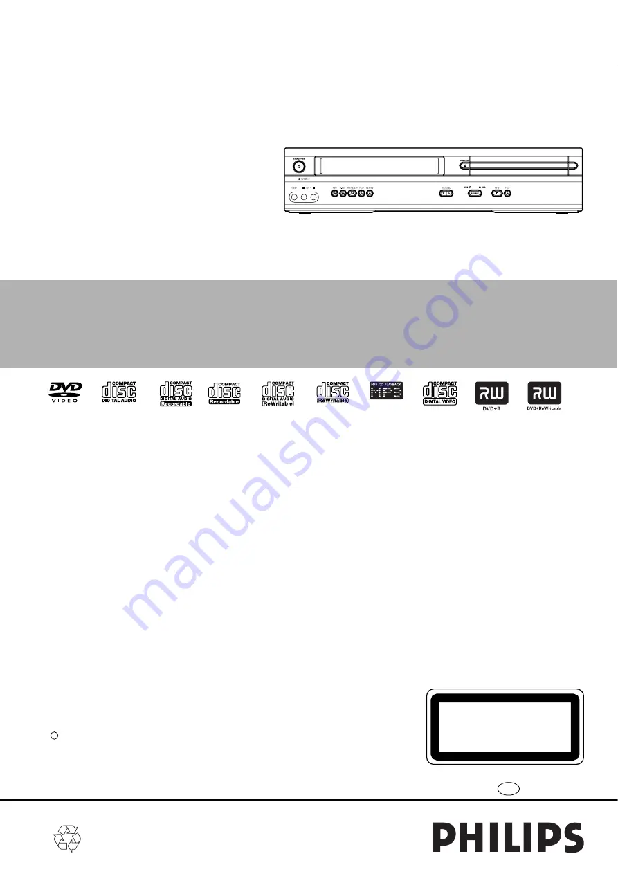
DVD + VCR Combi

DVP3050V

/75

 c Copyright 2005 Philips Consumer Electronics B.V. Eindhoven, The Netherlands

All rights reserved. No part of this publication may be reproduced, stored in a retrieval 
system or transmitted, in any form or by any means, electronic, mechanical, photocopying, 
or otherwise without the prior permission of Philips.

CLASS 1 LASER PRODUCT
KLASSE 1 LASER PRODUKT
KLASS 1 LASER APPARAT
CLASSE 1 PRODUIT LASER

GB    3139 785 31020


Service Manual

Service

Service

Service

Summary of Contents for DVP3050V/75

Page 1: ... Combi DVP3050V 75 c Copyright 2005 Philips Consumer Electronics B V Eindhoven The Netherlands All rights reserved No part of this publication may be reproduced stored in a retrieval system or transmitted in any form or by any means electronic mechanical photocopying or otherwise without the prior permission of Philips CLASS 1 LASER PRODUCT KLASSE 1 LASER PRODUKT KLASS 1 LASER APPARAT CLASSE 1 PRO...

Page 2: ...STMENT INSTRUCTIONS 1 9 1 HOW TO INITIALIZE THE DVD PLAYER VCR 1 10 1 FIRMWARE RENEWAL MODE 1 11 1 BLOCK DIAGRAMS 1 12 1 SCHEMATIC DIAGRAMS CBA S AND TEST POINTS 1 13 1 WAVEFORMS 1 14 1 WIRING DIAGRAM VCR SECTION 1 15 1 WIRING DIAGRAM DVD SECTION 1 15 2 SYSTEM CONTROL TIMING CHARTS 1 16 1 IC PIN FUNCTION DESCRIPTIONS 1 17 1 LEAD IDENTIFICATIONS 1 18 1 ELECTRICAL PARTS LIST 1 19 1 EXPLODED VIEWS 1 ...

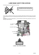
Page 3: ...is turned on Do not look directly at the laser beam CAUTION Use of controls and adjustments or doing procedures other than those specified herein may result in hazardous radiation exposure Location Top of DVD mechanism Do not look directly at the laser beam coming from the pickup or allow it to strike against your skin Drive Mechanism Assembly Laser Beam Radiation Laser Pickup Turntable CAUTION CL...

Page 4: ... especially 1 Wires covered with PVC tubing 2 Double insulated wires 3 High voltage leads D Use specified insulating materials for hazardous live parts Note especially 1 Insulation tape 2 PVC tubing 3 Spacers 4 Insulators for transistors E When replacing AC primary side components transformers power cord etc wrap ends of wires securely about the terminals before solder ing F Observe that the wires...

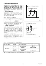
Page 5: ... termi nals antenna terminals video and audio input and output terminals microphone jacks earphone jacks etc is lower than or equal to the specified value in the table below Measuring Method Power ON Insert load Z between B earth ground power cord plug prongs and exposed accessible parts Use an AC voltmeter to measure across the terminals of load Z See Fig 2 and the following table AC Line Voltage...

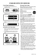
Page 6: ...lips SAC305 with order code 0622 149 00106 If lead free solder paste is required please contact the manufacturer of your solder equipment In general use of solder paste within workshops should be avoided because paste is not easy to store and to handle Use only adequate solder tools applicable for lead free solder alloy The solder tool must be able To reach at least a solder temperature of 400 C T...

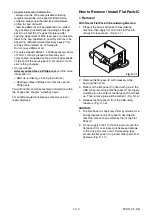
Page 7: ...nd other ICs used in Philips sets You will find this and more technical information within the magazine chapter workshop news For additional questions please contact your local repair helpdesk How to Remove Install Flat Pack IC 1 Removal With Hot Air Flat Pack IC Desoldering Machine 1 Prepare the hot air flat pack IC desoldering machine then apply hot air to the Flat Pack IC about 5 to 6 seconds F...

Page 8: ... solder flux which is applied to all pins of the flat pack IC you can remove it easily Fig S 1 3 2 Affix the wire to a workbench or solid mounting point as shown in Fig S 1 5 3 While heating the pins using a fine tip soldering iron or hot air blower pull up the wire as the solder melts so as to lift the IC leads from the CBA contact pads as shown in Fig S 1 5 4 Bottom of the flat pack IC is fixed ...

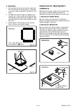
Page 9: ...ccur due to a potential difference caused by electrostatic charge during unpacking or repair work 1 Ground for Human Body Be sure to wear a grounding band 1 MΩ that is properly grounded to remove any static electricity that may be charged on the body 2 Ground for Workbench Be sure to place a conductive sheet or copper plate with proper grounding 1 MΩ on the workbench or other surface where the sem...

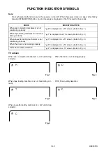
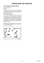
Page 10: ...ectly When the drum is not working properly P ON Power safety detection MODE INDICATOR ACTIVE When reel or capstan mechanism is not functioning correctly A R is displayed on a TV screen Refer to Fig 1 When tape loading mechanism is not func tioning correctly A T is displayed on a TV screen Refer to Fig 2 When cassette loading mechanism is not functioning correctly A C is displayed on a TV screen R...

Page 11: ...into the Deck Mechanism Assembly and press the PLAY button The tape will be loaded into the Deck Mechanism Assembly Make sure the power is on connect TP501 S INH to GND This will stop the function of Tape Start Sensor Tape End Sensor and Reel Sensors If these TPs are connected before plugging in the unit the function of the sensors will stay valid See Fig 1 Note Because the Tape End Sensors are in...

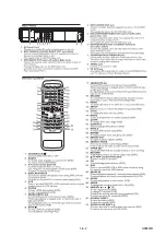
Page 12: ...1 6 1 H9923IB OPERATING CONTROLS AND FUNCTIONS ...

Page 13: ...1 6 2 H9923IB ...

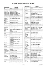
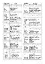
Page 14: ...apstan Motor FWD REV Control Signal FWD L REV H C FG Capstan Motor Rotation Detection Pulse C ROTA Color Phase Rotary Changeover SIgnal C SYNC Composite Synchronized Pulse CLKSEL Clock Select GND CTL Playback Record Control Signal CTL Playback Record Control Signal CTLAMP out To Monitor for CTL AMP Output D CONT Drum Motor Control Signal D PFG Drum Motor Phase Frequency Generator D REC H Delayed R...

Page 15: ...r On Signal P ON 5V 5V at Power On Signal P ON 9V 5V at Power On Signal Signal Name Function P ON H Power On Signal at High P61 LP P61 LP P80 C P80 C Terminal PG DELAY Video Head Switching Pulse Signal Adjusted Voltage POW SAF P ON Power Detection Input Signal POWER LED POWER LED Signal Output PWRCON IN Power Down REC LED REC LED Signal Output REC SAF SW Recording Safety SW Detect With Record tab ...

Page 16: ...EO Y I Component Video Luminance Signal Interlace VIDEO Y I P Component Video Luminance Signal Interlace Progressive VSS GND XCin Sub Clock XCOUT Sub Clock Xin Main Clock Input Xout Main Clock Input Signal Name Function ...

Page 17: ...No PART REMOVAL Fig No REMOVE UNHOOK UNLOCK RELEASE UNPLUG DESOLDER Note 1 Top Case D1 7 S 1 2 Front Assembly D2 3 L 1 3 L 2 1 1 1 1 2 3 Top Bracket D2 3 S 2 4 DVD Mechanism Assembly D3 4 S 3 CN401 CN601 5 Partition Plate D3 2 S 4 6 Loader Holder D3 2 S 5 1 Top Case 2 Front Assembly 3 Top Bracket 4 DVD Mechanism Assembly 7 DVD Main CBA Unit 15 Jack Board 5 Partition Plate 6 Loader Holder 8 VCR Cha...

Page 18: ...t Fig D4 2 2 Short the three short lands of FPC cable with sol der before removing the FFC cable CN201 from it If you disconnect the FFC cable CN201 the laser diode of pickup will be destroyed Fig D4 CAUTION 3 When reassembling confirm the FFC cable CN201 is connected completely Then remove the solder from the three short lands of FPC cable Fig D4 4 When reassembling solder wire jumpers as shown i...

Page 19: ... Mechanism Assembly CN401 CN601 S 3 S 3 S 3 S 4 S 5 Fig D3 CN201 CN301 S 6 7 DVD Main CBA Unit DVD Mechanism A Fig D4 S 6 View for A Short the three short lands by soldering Either of two places Connector S 7 S 7 S 8 S 8 S 9 S 9 Fig D5 8 VCR Chassis Unit ...

Page 20: ...lder Lead with blue stripe From FE Head BOTTOM VIEW Lead connections of Deck Assembly and Main CBA Desolder From Capstan Motor Assembly Printing side Desolder From Cylinder Assembly From ACE Head Assembly Lead with blue stripe Lead with blue stripe Desolder Lead with red stripe 12 Main CBA SW507 LD SW LD SW Pin Hole Hole Shaft Cam Gear 12 Main CBA 9 Deck Assembly Pin Desolder Lead with blue stripe...

Page 21: ... Mechanism HOW TO EJECT MANUALLY 1 Remove the Top Case Front Assembly and Top Bracket 2 Remove four Screws S 3 in Fig D3 Do not disconnect connectors 3 While lifting up the DVD Mechanism rotate the roulette in the direction of the arrow as shown below 4 Pull the tray slowly manually ...

Page 22: ...e with 10 1 probe V Range 0 001 50V Div F Range DC AC 20MHz 2 Alignment Tape 9965 000 14514 Head Switching Position Adjustment Purpose To determine the Head Switching position during playback Symptom of Misadjustment May cause Head Switching noise or vertical jitter in the picture Reference Notes Playback the Alignment tape and adjust VR501 so that the V sync front edge of the CH1 video output wav...

Page 23: ...ntrol unit in that order Fig a appears on the screen 2 Press CLEAR C RESET button on the remote control unit Fig b appears on the screen When OK appears on the screen the factory default will be set 3 To exit this mode press STANDBY ON button MODEL Version Region EXIT POWER EEPROM CLEAR CLEAR Fig a differ depending on the models MODEL Version Region EEPROM CLEAR OK EXIT POWER EEPROM CLEAR CLEAR di...

Page 24: ...ppears on the VFD Fig f At this time no button is available 6 Remove the disc on the tray 7 Unplug the AC cord from the AC outlet Then plug it again 8 Turn the power on by pressing the STANDBY ON button and the tray will close 9 Press DVD 1 2 3 4 and DISPLAY STATUS buttons on the remote control unit in that order Fig g appears on the screen No Appearance State 1 Reading Sending files into the memo...

Page 25: ...h appears on the screen When OK appears on the screen the factory default will be set Then the firmware renewal mode is complete 11 To exit this mode press STANDBY ON button MODEL Version Region EEPROM CLEAR OK EXIT POWER EEPROM CLEAR CLEAR differ depending on the models Fig h ...

Page 26: ...TEM CONTROL AUDIO MUTE H 5 6 SENSOR CBA SENSOR CBA END S ST S Q504 Q503 REC SAFETY END S CTL 97 TP503 CTL 79 23 POWER SW651 POWER TO DVD SYSTEM CONTROL SERVO BLOCK DIAGRAM DVD SECTION TO DVD SYSTEM CONTROL SERVO BLOCK DIAGRAM DVD SECTION CN502 C FG C CONT D PFG C F R 90 76 87 78 LM FWD REV 81 D CONT 77 AL 12V 1 P ON 15V P ON 5V 1 AL 12V 1 2 P ON 5V 3 C FG 4 C F R 5 C CONT 6 GND 7 LM FWD REV 8 D CO...

Page 27: ...HARACTER MIX 29 24 23 94 28 10 27 11 D REC H 30 BUFFER Q305 DVD VCR TP751 V OUT WF3 TP301 C PB WF2 VIDEO OUT VIDEO IN MAIN CBA TP504 RF SW WF1 OUTPUT SELECT DVD VIDEO TO SERVO SYSTEM CONTROL BLOCK DIAGRAM C SYNC C SYNC 93 IC751 OUTPUT SELECT 4 11 10 9 SW CTL TUNER UNIT MODE SP REC PB VIDEO SIGNAL DVD VIDEO SIGNAL JK752 TO DVD VIDEO AUDIO BLOCK DIAGRAM DVD SECTION IC1404 REAR JK751 FRONT 3 5 JK753 ...

Page 28: ...OM 1 AE H 2 AE H FE H AUDIO HEAD AUDIO ERASE HEAD ACE HEAD ASSEMBLY FE HEAD 2 FE H 1 FE H GND CN501 MAIN CBA PB AUDIO SIGNAL REC AUDIO SIGNAL Mode SP REC 10 D REC H AUDIO MUTE H FULL ERASE HEAD 23 24 SERIAL DECODER DECK ASSEMBLY LINE1 LINE2 80 AUDIO IN F IIC BUS SCL IIC BUS SDA TO SERVO SYSTEM CONTROL BLOCK DIAGRAM SMD NOTE FOR WIRE CONNECTORS 1 PREFIX SYMBOL CN MEANS CONNECTOR CAN DISCONNECT AND ...

Page 29: ...DIO SIGNAL AFV CBA TU AUDIO R 4 TU AUDIO L 5 4 5 CN701 CN1 CN701 CN1 TU701 TUNER UNIT SIF OUT AUDIO IN 22 2 MUTE ON MUTE ON REAR TO DVD VIDEO AUDIO BLOCK DIAGRAM DVD SECTION FRONT JK756 AUDIO R IN AUDIO R IN AUDIO L IN AUDIO L IN JK751 IC751 OUTPUT SELECT 12 13 14 15 2 1 11 10 9 SW CTL VCR DVD VCR DVD OUTPUT SELECT TO DVD VIDEO AUDIO BLOCK DIAGRAM DVD SECTION 44 47 6 49 63 Hi Fi AUDIO R HEAD Hi Fi...

Page 30: ... 2V REG FL EV 3 3V DVD P ON 3 3V DVD P ON 5V Q1055 CN1051 SW 5V Q1052 SW 3 3V Q058 Q057 SW 5V HOT COLD NOTE FOR WIRE CONNECTORS 1 PREFIX SYMBOL CN MEANS CONNECTOR CAN DISCONNECT AND RECONNECT 2 PREFIX SYMBOL CL MEANS WIRE SOLDER HOLES OF THE PCB WIRE IS SOLDERED DIRECTLY CAUTION Fixed voltage or Auto voltage selectable power supply circuit is used in this unit If Main Fuse F1001 is blown check to ...

Page 31: ...OR M SPINDLE MOTOR MICRO CONTROLLER SLED MOTOR DRIVE FOCUS ACTUATOR DRIVE SPINDLE MOTOR DRIVE TRACKING ACTUATOR DRIVE 147 TRAY IN SLD 75 72 SPDL 76 TRACKING DRIVE 148 FOCUS DRIVE TO DIGITAL SIGNAL PROCESS BLOCK DIAGRAM FS FS TS TS TO DVD VIDEO AUDIO BLOCK DIAGRAM 57 ADAC MD 56 ADAC MC 86 ADAC ML ADAC MC ADAC ML PCM SCLK 88 AUDIO MUTE ADAC MD AUDIO MUTE 163 PCM SCLK I P SW 183 I P SW TRAY IN 3 SP 4...

Page 32: ... INST ROM DATA RAM INST ROM SERIAL D A GENERAL I O INTERRUPT CONTROLLER TIMER WATCH DOG TIMER REMOTE CONTROL 32BIT CPU STREAM I F EXTERNAL MEMORY I F SDRAM ECC UMAC 114 115 116 117 132 131 134 133 129 130 126 124 125 123 83 DEBUG BCU INST RAM DATA RAM D A D A D A TO DVD VIDEO AUDIO BLOCK DIAGRAM 156 158 VIDEO Y I VIDEO C VIDEO Pr Cr VIDEO Pb Cb TO DVD VIDEO AUDIO BLOCK DIAGRAM 177 SPDIF 170 PCM BC...

Page 33: ...IVER WF6 IC601 AUDIO DAC 15 14 1 16 DIGITAL AUDIO OUT COAXIAL JK1202 BUFFER Q1351 IC1201 AUDIO 5V AMP CN601 CN1601 13 13 DVD AUDIO L 15 15 DVD AUDIO R 14 14 DVD AUDIO R MUTE 7 6 8 4 3 2 5 FROM DVD SYSTEM CONTROL SERVO BLOCK DIAGRAM FROM DIGITAL SIGNAL PROCESS BLOCK DIAGRAM SERIAL PORT SERIAL CONTROL 4X 8X OVERSAMPLING DIGITAL FILTER FUNCTION CONTROLLER ENPHANCED MULTI LEVEL DELTA SIGMA MODULATOR D...

Page 34: ...iginal function and reliability of repaired units use only original replacement parts which are listed with their part numbers in the parts list section of the service manual 3 How to read converged lines 4 All resistance values are indicated in ohms K 103 M 106 5 Resistor wattages are 1 4W or 1 6W unless other wise specified 6 All capacitance values are indicated in µF P 10 6 µF 7 All voltages ar...

Page 35: ... 4 R549 C 1 C531 E 4 R552 C 1 C533 E 4 R556 C 4 C534 D 4 R557 C 4 C535 D 4 R558 C 4 C538 D 4 R567 D 4 C539 D 3 R568 E 4 C540 D 3 R569 E 4 C541 E 2 R570 D 1 C542 E 2 R572 D 4 C543 E 2 R574 D 2 C544 E 2 R575 D 2 C545 E 3 R577 D 3 C546 E 3 R578 D 3 C547 E 3 R582 E 2 C548 E 2 R585 E 2 C549 E 2 R586 E 2 C550 E 2 R588 F 3 C553 E 2 R590 C 1 C555 E 4 R592 A 3 R594 A 3 CN501 A 2 R596 A 3 CN502 F 4 CN504 A ...

Page 36: ... 0 2 5 0 5 0 The same voltage for PLAY REC DVD modes Indicates that the voltage is not consistent here 1 13 3 IC501 KEY VOLTAGE CHART 0 00 0 51V REC OTR 0 51 0 92V STOP EJECT 0 92 1 27V OUTPUT SELECT PLAY 1 27 1 61V REW 1 61 1 98V FF 1 98 2 39V CH UP SENS INH 2 39 2 90V CH DOWN 2 90 3 60V 3 60 4 30V DIRECT DUBBING 4 30 5 00V KEY OFF KEY OFF Pin No Voltage KEY 1 7 PIN KEY 2 8 PIN ...

Page 37: ... A A 5G 4G 3G 2G 1G 7G 6G a d g c b e f f i i REPEAT TITLE GROUP VCR CHP REC SACD TRK A ALL B PSCAN DVD PM HDVCD A Main 2 8 Sensor Power SW Schematic Diagram VCR Section SMD PLAY mode REC mode DVD mode Voltage indications for PLAY REC and DVD modes on the Schematic Diagrams are as shown below 1 2 3 5 0 2 5 0 5 0 The same voltage for PLAY REC DVD modes Indicates that the voltage is not consistent h...

Page 38: ...1 G 1 R615 G 4 R616 G 3 CN509 K 2 R617 J 3 CN701 L 1 R618 J 4 R621 J 3 D502 H 3 R622 J 3 D503 H 3 R624 I 4 D613 H 4 R701 H 1 D701 G 2 R702 H 1 R703 G 2 IC611 J 4 R706 H 1 IC612 J 3 R707 H 1 R714 G 1 L701 I 2 L702 H 2 SW501 J 1 SW503 J 1 R501 J 1 SW504 J 1 R502 J 1 SW507 J 2 R503 J 1 SW601 K 2 R504 J 1 SW602 J 2 R505 K 1 SW603 J 2 R511 J 2 SW604 J 2 R514 J 2 SW605 J 2 R516 J 2 R519 J 2 TU701 H 2 R5...

Page 39: ... 1 C409 N 2 R253 N 2 R406 N 2 C315 Q 1 C410 M 1 R256 N 2 R408 N 2 C318 Q 2 C411 N 1 R257 N 2 R409 N 2 C319 Q 2 C412 N 1 R302 O 1 R410 M 1 C320 Q 2 C413 O 2 R303 O 2 R414 N 2 C321 Q 2 C414 O 1 R304 O 2 R415 N 2 C323 Q 2 C416 N 4 R305 O 1 R416 N 2 C324 Q 2 C420 N 4 R306 O 1 R417 N 1 C326 Q 2 C421 N 4 R307 O 1 R418 N 1 C328 Q 3 C422 N 4 R308 O 1 R419 O 2 C330 Q 3 C423 N 4 R309 O 1 R420 O 2 C331 Q 3 C...

Page 40: ...tion SMD PLAY mode REC mode DVD mode Voltage indications for PLAY REC and DVD modes on the Schematic Diagrams are as shown below 1 2 3 5 0 2 5 0 5 0 The same voltage for PLAY REC DVD modes Indicates that the voltage is not consistent here 1 13 7 ...

Page 41: ...245 T 2 R1209 T 1 C1246 T 1 R1210 T 1 C1247 T 1 R1211 T 1 C1249 T 2 R1221 U 1 C1353 W 2 R1222 U 1 C1354 W 1 R1223 V 1 C1355 W 1 R1224 V 1 C1359 V 1 R1227 V 1 C1393 S 1 R1228 V 1 C1394 S 1 R1238 U 2 C1421 T 4 R1240 U 1 C1422 W 3 R1245 T 2 C1423 T 3 R1352 V 1 C1441 T 4 R1353 W 2 C1442 W 3 R1354 V 1 C1445 V 2 R1355 W 1 C1461 T 2 R1356 W 1 C1462 V 2 R1361 W 1 C1471 T 3 R1394 S 1 C1481 T 2 R1396 S 1 C1...

Page 42: ...Ref No Position C752 Y 3 C753 Z 2 C754 Z 3 C756 Z 3 C757 Z 3 C770 AC 1 C771 AC 1 C774 AC 3 C776 AC 2 C777 AC 2 IC751 Z 4 IC1404 AA 4 Q305 Z 3 Q770 AB 2 Q771 AA 2 R752 Y 3 R754 AB 3 R755 AC 3 R756 AC 1 R757 Y 3 R758 Z 3 R759 Z 3 R760 AA 4 R761 AA 3 R762 AA 4 R763 AA 4 R770 AC 1 R771 AC 1 R772 AB 2 R773 AA 2 R774 AC 3 R775 AC 3 R776 AC 3 R777 AC 2 R778 AC 1 R779 AC 1 JK751 AC 3 JK752 AC 3 JK753 AC 1...

Page 43: ...VCR Section SMD PLAY mode REC mode DVD mode Voltage indications for PLAY REC and DVD modes on the Schematic Diagrams are as shown below 1 2 3 5 0 2 5 0 5 0 The same voltage for PLAY REC DVD modes Indicates that the voltage is not consistent here 1 13 10 ...

Page 44: ...I 2 R1061 AG 1 CN1051 AE 3 R1062 AF 1 R1065 AF 1 D054 AH 3 R1066 AF 1 D056 AI 4 R1067 AF 1 D057 AH 3 R1068 AG 1 D058 AG 3 R1071 AE 1 D1052 AF 2 R1072 AF 1 D1053 AF 2 R1085 AE 3 D1054 AF 2 R1086 AE 3 D1057 AG 1 R1087 AF 3 R1090 AG 3 IC1002 AF 3 R1091 AG 2 IC1003 AF 3 R2001 AH 1 R2002 AI 2 L053 AG 3 R2003 AH 2 L751 AI 2 R2005 AI 1 L2001 AI 1 R2006 AI 2 R2082 AH 2 Q053 AH 4 R2083 AI 2 Q054 AH 4 R2086...

Page 45: ... R1001 AK 3 C1107 AN 2 R1002 AL 2 C2014 AM 3 R1003 AL 2 C2015 AN 2 R1004 AM 3 R1005 AL 3 D013 AN 4 R1006 AL 3 D014 AN 4 R1007 AL 3 D016 AN 3 R1008 AL 3 D017 AN 4 R1010 AM 3 D018 AN 3 R1011 AM 3 D1001 AL 4 R1020 AN 1 D1002 AL 3 R1021 AN 1 D1003 AL 4 R1022 AN 1 D1004 AL 3 R1023 AN 1 D1006 AM 3 R1025 AN 1 D1008 AN 2 R1029 AL 3 D1011 AM 3 R1032 AL 2 D1012 AM 3 R1035 AM 2 D1016 AN 2 R1036 AL 2 D1017 AN...

Page 46: ...N For continued protection against fire hazard replace only with the same type fuse NOTE The voltage for parts in hot circuit is measured using hot GND as a common terminal CAUTION Fixed voltage or Auto voltage selectable power supply circuit is used in this unit If Main Fuse F1001 is blown check to see that all components in the power supply circuit are not defective before you connect the AC plu...

Page 47: ... R451 AQ 1 C454 AR 2 R452 AQ 1 C455 AR 2 R453 AS 3 C456 AR 2 R454 AS 3 C457 AR 2 R455 AS 3 C458 AR 2 R458 AQ 4 C459 AR 2 R459 AQ 4 C461 AR 2 R460 AP 3 C462 AS 3 R461 AP 3 C463 AR 3 R462 AP 3 C464 AS 3 R463 AP 3 C465 AR 4 R464 AP 3 C466 AR 4 R465 AQ 2 C467 AR 3 R466 AP 2 C468 AR 3 R467 AP 3 C469 AR 3 R470 AQ 3 C470 AR 3 R471 AP 3 C471 AQ 3 R472 AP 2 C472 AQ 3 R473 AP 2 C473 AQ 3 R474 AQ 1 C474 AP 4...

Page 48: ...Auto voltage selectable power supply circuit is used in this unit If Main Fuse F1001 is blown check to see that all components in the power supply circuit are not defective before you connect the AC plug to the AC power supply Otherwise it may cause some components in the power supply circuit to fail Because a hot chassis ground is present in the power supply circut an isolation transformer must b...

Page 49: ...oltage selectable power supply circuit is used in this unit If Main Fuse F1001 is blown check to see that all components in the power supply circuit are not defective before you connect the AC plug to the AC power supply Otherwise it may cause some components in the power supply circuit to fail Because a hot chassis ground is present in the power supply circut an isolation transformer must be used...

Page 50: ...ISTORS RESISTORS RESISTORS SWITCHES VARIABLE RESISTOR C315 C 3 C465 B 3 C704 A 4 C1442 F 4 D1053 G 2 Q403 C 3 C318 C 3 C466 B 3 C705 A 4 C1445 E 4 D1054 G 2 Q405 C 3 C319 C 2 C467 B 3 C706 A 4 C1461 E 3 D1057 F 1 Q506 C 2 C320 C 2 C468 B 3 C711 A 3 C1462 E 4 D1301 C 4 Q515 B 1 C321 C 3 C469 A 3 C714 A 4 C1471 E 3 Q770 F 4 C323 B 2 C470 A 3 C716 A 2 C1481 E 3 IC301 C 3 Q771 F 4 C324 C 2 C471 A 3 C7...

Page 51: ...Power SW CBA Top View BH99A0F01011B Power SW CBA Bottom View BH99A0F01011C DVD Open Close CBA Top View DVD Open Close CBA Bottom View 1 13 18 ...

Page 52: ... B 1 C17 A 2 R4 B 2 C19 A 2 R5 A 1 C20 A 2 R6 A 1 C21 A 1 C22 A 2 X1 B 1 C24 B 2 C27 C 2 CRYSTAL OSCILLATOR COILS DIODE RESISTORS CONNECTOR IC CAPACITORS AFV CBA Parts Location Guide Ref No Position Ref No Position C1 A 2 CN1 B 1 C4 A 2 C5 A 2 D2 B 2 C6 A 2 C7 A 2 IC1 B 2 C8 A 2 C11 A 2 L1 A 1 C12 A 2 L2 B 2 C13 A 1 L3 A 2 C14 A 1 L4 A 2 C15 B 1 C16 B 1 R1 A 2 C17 B 1 R4 B 2 C19 A 1 R5 A 1 C20 A 1...

Page 53: ...Y mode STOP mode Voltage indications for PLAY and STOP modes on the Schematic Diagrams are as shown below 1 2 5 0 The same voltage for both PLAY STOP modes Indicates that the voltage is not consistent here 1 NOTE Either IC461 or IC462 is used for DVD MAIN CBA UNIT 1 13 20 ...

Page 54: ...DVD Section SMD 3 5 0 2 5 PLAY mode STOP mode Voltage indications for PLAY and STOP modes on the Schematic Diagrams are as shown below 1 2 5 0 The same voltage for both PLAY STOP modes Indicates that the voltage is not consistent here 1 13 21 ...

Page 55: ...2 3 2 3 32 64 0 0 96 128 1 7 1 7 PIN NO PLAY STOP PIN NO PLAY STOP PIN NO PLAY STOP PIN NO PLAY STOP 129 2 3 2 3 161 3 4 3 4 193 225 3 4 3 4 130 2 3 2 3 162 0 0 194 226 131 2 3 2 3 163 1 8 1 8 195 227 132 2 4 2 3 164 0 0 196 3 4 3 4 228 133 2 4 2 4 165 1 7 1 8 197 229 0 0 134 2 4 2 4 166 1 7 1 7 198 230 135 2 3 2 3 167 3 4 3 4 199 231 3 4 3 4 136 2 3 2 3 168 0 0 200 232 1 3 1 6 137 2 3 2 3 169 1 8...

Page 56: ...DVD Section SMD 3 5 0 2 5 PLAY mode STOP mode Voltage indications for PLAY and STOP modes on the Schematic Diagrams are as shown below 1 2 5 0 The same voltage for both PLAY STOP modes Indicates that the voltage is not consistent here 1 13 23 ...

Page 57: ...1µs Pin 8 of CN1601 Pin 10 of CN1601 Pin 13 of CN1601 Pin 15 of CN1601 Pin 18 of CN1601 NOTE Input VCR COLOR BAR SIGNAL WITH 1KHz AUDIO SIGNAL WF1 WF3 DVD POWER ON STOP MODE WF4 WF6 CD 1kHz PLAY WF7 WF9 AUDIO R 1V 0 5ms V OUT E E 0 2V 20µs V OUT 10V 50µs RF SW 0 5V C PB RF SW 0 2V 5ms 10V VIDEO Y 0 2V 20µs VIDEO C 0 2V 20µs VIDEO CVBS 0 5V 20µs 1 14 1 H9923WF ...

Page 58: ...D PWRCON FP CLK FP DIN FP STB REMOTE DVD FP DOUT NU 23 24 25 26 DVD POWER DVD OPEN CLOSE DVD STOP 27 OUTPUT SELECT DVD PLAY VIDEO Pr Cr I P SW 1 VIDEO Y I ASPECT NU VIDEO Pb Cb GND GND VIDEO Y I P GND VIDEO C GND GND DVD AUDIO L DVD AUDIO R MUTE DVD AUDIO R AUDIO 5V AUDIO 5V SPDIF TO WIRING DIAGRAM DVD SECTION GND 1 KEY 1 2 3 POWER LED 1 2 3 AFV CBA DVD OPEN CLOSE CBA SIF 1 NU 2 TU AUDIO R 3 GND 4...

Page 59: ...01 1 2 3 4 5 6 7 8 9 10 11 12 13 14 15 16 17 18 19 20 TS TS FS CD LD FS GND DVD PD GND CD PD PD MONI DVD LD VREF E GND B DVD P ON 5V CD DVD D A C F GND LD DETECTOR FS TS 7 9 11 2 3 6 5 4 2 3 4 5 6 7 8 9 10 11 12 13 14 15 16 17 18 19 20 21 22 EV 1 2V EV 1 2V EV 3 3V EV 3 3V EV 3 3V DVD P ON 3 3V DVD P ON 5V EV 11V EV 11V GND GND GND GND GND GND GND PWRCON REMOTE DVD 23 24 25 26 DVD POWER DVD OPEN C...

Page 60: ... 2 17V SF 1 51V 1 98V 1 80V SM 3 20V 3 75V 3 40V AU 0 26V 0 65V 0 44V AL 4 51V 5 00V 5 00V SS 2 61V 3 19V 2 97V RS Note EJ RS Loading FWD LM FWD REV H RS EJ Loading REV LM FWD REV L Stop A Loading Stop B Unloading Note Symbol Loading Status EJ Eject CL Eject REW Reel SB REW Reel Stop B TL Stop B Brake Cancel FB Brake Cancel FF REW SF FF REW Stop M FF REW SM Stop M FF REW Stop A AU Stop A Play REC ...

Page 61: ...de Fig 1 18 RF SW F AD Internal Signal C DRIVE PB CTL 78 C F R 16 H A SW 15 C ROTA The first rise of RF SW after a rise in F AD signal Acceleration Detection T1 AT H Z H L L Stop detection T2 ST Slow Tracking Value BL Reversal Limit Value STILL FRAME ADVANCE STILL 20ms ...

Page 62: ...D Internal Signal C DRIVE PB CTL 78 C F R 16 H A SW 15 C ROTA H Z H L L STILL STILL AT ST BL Stop detection T2 Acceleration Detection T1 Slow Tracking Value Reversal Limit Value FRAME ADVANCE The first rise of RF SW after a rise in F AD signal 20ms ...

Page 63: ...LD REV LD REV LD REV 0 2S 0 5S PIN NO CL EJ SS SS AU AU TL LD SW CL SS LM FWD M REV C DRIVE Z ON ON C F R DRUM ROTATION P ON H A MUTE H D REC H D PB PAUSE SLOW AU AL AL AU SF SM EJ AU RS SF SM TL FB AL SB 9 81 78 73 83 33 TV VCR POWER OFF STOP PLAY RS FS STILL SLOW PLAY STOP PLAY DISPLAY 0 1S SB TL SB FB SM SM SF AL AL RS AU AL SS AU AL SM 0 8S 0 2S 0 3S 1 0S 0 2S 1 5S 2H 2 5S 4H 0 5S 0 2S 0 8S 2H...

Page 64: ...JECT STOP A LD REV FF LD REV LD REV LD FWD LD FWD LD FWD LD FWD LD FWD LD FWD LD FWD REC PAUSE REC REC REW LD REV LD REV LD REV LD REV LD REV LD REV LD REV PAUSE REC or PAUSE STOP EJECT STOP EJECT STOP EJECT 2 STOP A FF STOP A REW STOP A REC PAUSE PAUSE or REC STOP A EJECT STOP FF STOP REW STOP REC REC REC PAUSE STOP TL TL SM SM SF SF AL AL SM AL AL AL AU AU SM TL SB EJ RS RS SM SM SF FB SM AU AU ...

Page 65: ... Section Tray IN TL221 Sled Drive TP303 Disc Drive TP301 Focus Drive TP304 Tracking Drive TP302 0V 3 3V 0V 1 65V 0V 0V 0V 1 65V 1 65V 1 65V Tray Close Play Play Tray Open Tray Close Disc Rotation Play Disc Stop Tray Open ...

Page 66: ...o Head Switching Pulse H L 20 NU Not Used 21 OUT TUNER SW1 Tuner System Control Signal Output H 22 OUT TUNER SW2 Tuner System Control Signal Output H 23 OUT POWER LED POWER LED Signal Output H L 24 OUT POWER LED POWER LED Signal Output H L 25 NU Not Used 26 NU Not Used 27 NU Not Used 28 NU Not Used 29 NU Not Used 30 NU Not Used 31 IN REC SAF SW Recording Safety SW Detect With Record tab L With out...

Page 67: ...r Signal P off L P on H H L 76 OUT C CONT Capstan Motor Control Signal PWM 77 OUT D CONT Drum Motor Control Signal PWM 78 OUT C F R Capstan Motor FWD REV Control Signal FWD L REV H H L 79 OUT OUTPUT SELECT Output Select H L 80 IN T REEL Take Up Reel Rotation Signal PULSE 81 OUT LM FWD REV Loading Motor Control Signal H L Hi z 82 NU Not Used Pin No IN OUT Signal Name Function Active Level 83 OUT AU...

Page 68: ...Strobe 3 NU Not Used 4 NU Not Used 5 VSS GND 6 VDD Power Supply 7 OUT a Segment Output 8 b 9 c 10 d 11 e 12 f 13 g 14 h 15 VEE Pull Down Level 16 OUT i Segment Output 17 OUT 7G Grid Output 18 6G 19 5G 20 4G 21 3G 22 2G 23 1G 24 VDD Power Supply 25 VSS GND 26 IN OSC Oscillator Input 27 NU Not Used 28 IN FP DIN Serial Data Input ...

Page 69: ... TC4053BF N 1 MID 32A22F PT204 6B 12 E C 35 7 BT 298NYM 1 5 4 8 1 BR24L02F WE2 CAT24WC02WI TE13 28 15 14 PT6313 S TP L SC16313G 1 B1 E B2 C1 C2 FMG4A T148 RN1511 TE85R RN1511 TE85R F KTC3875S Y RTK P C B E 60 LA72638M 21 40 41 20 1 80 61 8 5 4 1 MM1636XWRE 2SA1015 GR TPE2 2SA1015 GR TE2 F T 2SC1815 BL TPE2 2SC1815 GR TPE2 2SC1815 BL TE2 F T 2SC1815 GR TE2 F T 2SC1815 Y TE2 F T 2SC1815 Y TPE2 2SC21...

Page 70: ...03 9965 000 19590 TACT SWITCH TC 1104 H 9 5 SW604 4822 276 13954 KSM0614B SW604 4822 276 14127 SKQSAF001A SW604 9965 000 19590 TACT SWITCH TC 1104 H 9 5 SW605 4822 276 13954 KSM0614B SW605 4822 276 14127 SKQSAF001A SW605 9965 000 19590 TACT SWITCH TC 1104 H 9 5 SW2021 4822 276 13954 KSM0614B SW2021 4822 276 14127 SKQSAF001A SW2021 9965 000 19590 TACT SWITCH TC 1104 H 9 5 SW2022 4822 276 13954 KSM0...

Page 71: ...000 23990 CHOKE COIL 47UH K L1012 9965 000 27579 FIXED INDUCTORS LGB0810T 470K L1251 9965 000 15331 INDUCTOR 0 47UH K 26T L1351 4822 157 10649 100UH L1521 9965 000 29480 CHOKE COIL 47UH L1521 9965 000 29481 RADIAL TYPE CHOKE COIL CW68 470K L1521 9965 000 05627 CHOKE COIL 47UH K L1521 9965 000 05702 CHOKE COIL 47UH K L1521 9965 000 23990 CHOKE COIL 47UH K L1521 9965 000 27579 FIXED INDUCTORS LGB081...

Page 72: ...ANSISTOR BN1L4M T Q058 9965 000 29490 TRANSISTOR KTA1267Y AT P Q058 9965 000 29491 TRANSISTOR KTA1267 GR AT P Q058 4822 130 11646 2SA1175J Q058 9965 000 19587 TRANSISTOR 2SA1175 H Q058 9965 000 05644 TRANSISTOR 2SA1175 F Q058 4822 130 63144 2SA1267 YG Q058 4822 130 10462 KTA1267 GR Q301 9965 000 29484 TRANSISTOR KTC3199 Y AT P Q301 9965 000 29485 TRANSISTOR KTC3199 GR AT P Q301 4822 130 41306 2SC1...

Page 73: ...TA1267 GR AT P Q1053 4822 130 11646 2SA1175J Q1053 9965 000 19587 TRANSISTOR 2SA1175 H Q1053 9965 000 05644 TRANSISTOR 2SA1175 F Q1053 4822 130 63144 2SA1267 YG Q1053 4822 130 10462 KTA1267 GR Q1054 9965 000 29484 TRANSISTOR KTC3199 Y AT P Q1054 9965 000 29485 TRANSISTOR KTC3199 GR AT P Q1054 4822 130 41306 2SC1815GR Q1054 9965 000 29486 TRANSISTOR 2SC1815 Y TE2 F T Q1054 9965 000 29487 TRANSISTOR...

Page 74: ...00 13852 IC SWITCH TC4053BF N OR IC1404 9965 000 02111 BU4053BCF IC1404 9965 000 23979 MULTIPLEXERS CD4053BCSJX IC1404 9965 000 23979 MULTIPLEXERS CD4053BCSJX POWER SWITCH CBA D651 9965 000 08621 LED RED 204HD E SW651 4822 276 13954 KSM0614B SW651 4822 276 14127 SKQSAF001A SW651 9965 000 19590 TACT SWITCH TC 1104 H 9 5 DVD OPEN CLOSE CBA SW2020 4822 276 13954 KSM0614B SW2020 4822 276 14127 SKQSAF0...

Page 75: ... are included in 1B2 DVD mechanism 2L021 AC1001 See Electrical Parts List for parts with this mark Some Ref Numbers are not in sequence A10 2B40 2L022 2L022 2L053 2B33 2B3 2L011 Sensor CBA Sensor CBA A4 A5 2B15 DVD Open Close CBA Power SW CBA JW001 JW004 JW003 2L091 2L054 2L054 2L012 2L023 2L023 2L082 B Main CBA 2B13 2L062 A F1001 JW002 2B11 2B18 2B15 AFV CBA 1B1 2L071 2L071 2L071 2L071 2B20 2L023...

Page 76: ...1 20 2 H9923PEX Packing Q U I C K FRONT Some Ref Numbers are not in sequence S2 S2 S2 S2 S1 Unit S3 A14 X4 X20 X5 X2 X3 X17 X1 X26 S9 ...

Page 77: ...9965 000 27556 DVD MECHA E6160 FG LESS A1X 9965 000 29466 FRONT ASSEMBLY H9923AD A2 9965 000 29467 TOP CASE D5 PAL FTZ H9700ED A22 9965 000 17140 CHASSIS FOOT H79P9JD X1 9965 000 29559 REMOTE CONTROL X3 4822 322 10137 RF CABLE LP PAL 960601 X3 4822 320 50377 CONNECT CABLE PAL X5 9965 000 24112 AV CORD TSCKA Y RW100 X5 9965 000 27558 AV CORD RCA M 2 TO RCA M 2 Note Alternative parts Only the parts ...

Reviews: