
Published by WO 0472 Service PaCE
Printed in the Netherlands
Subject to modification
EN 3122 785 14590
©
Copyright 2004 Philips Consumer Electronics B.V. Eindhoven, The Netherlands.
All rights reserved. No part of this publication may be reproduced, stored in a
retrieval system or transmitted, in any form or by any means, electronic,
mechanical, photocopying, or otherwise without the prior permission of Philips.
Colour Television
Chassis
EM5.2E
AA
E_14590_000.eps
240304
Contents
Page
Contents
Page
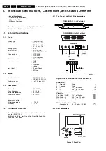
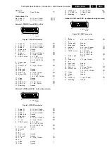
1.
Technical Specifications, Connections,
and Chassis Overview
2
2.
Safety Instructions, Warnings, and Notes
5
3.
Directions for Use
7
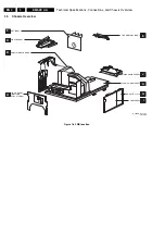
4.
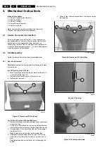
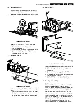
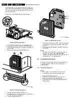
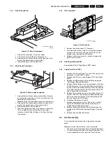
Mechanical Instructions
8
5.
Service Modes, Error Codes, and Faultfinding
12
6.
Block Diagrams, Test Point Overviews,
and Waveforms
Wiring Diagram
23
Block Diagram Supply and Deflection
24
Testpoint Overview LSP and CRT Panel
25
Block Diagram Video
26
Testpoint Overview SSB
27
Block Diagram Audio 1 (excl. Wireless Audio
Details)
28
I
2
C-IC Overview
29
Supply Lines Overview
30
7.
Circuit Diagrams and PWB Layouts
Diagram PWB
Main Supply
(Diagram A1) 31
40-45
Stand-by Supply
(Diagram A2) 32
40-45
Line Deflection
(Diagram A3) 33
40-45
Frame Deflection & E/W Drive
(Diagram A4) 34
40-45
Rotation Circuitry
(Diagram A5) 35
40-45
Audio Amplifier
(Diagram A6) 36
40-45
Tuner SIMM connector (Female) (Diagram A8) 37
40-45
Receiver
(Diagram A9) 38
40-45
Front
(Diagram A10) 38
40-45
Inputs/Outputs
(Diagram A11) 39
40-45
SIMM connector (Male)
(Diagram B1) 46
56-61
IF, I/O Videoprocessing
(Diagram B2) 47
56-61
PICNIC
(Diagram B3A) 48
56-61
Falconic (FEM)
(Diagram B3B) 49
56-61
Eagle
(Diagram B3C)50
56-61
HOP
(Diagram B4) 51
56-61
OTC
(Diagram B5A) 52
56-61
Anti Moiré
(Diagram B5B) 53
56-61
Audio Demodulator
(Diagram B6) 54
56-61
Headphone Amplifier
(Diagram B10) 55
56-61
Side I/O Panel (PV02)
(Diagram D)
62
63
Side I/O Panel (FL13B)
(Diagram D)
64
65
Top Control Panel (PV02)
(Diagram E)
66
66
Top Control Panel (FL13B)
(Diagram E)
67
68
CRT Panel
(Diagram F)
69
70
DC Shift Panel
(Diagram G)
71
71
I/O 3rd SCART Panel (PV02)
(Diagram H)
72
73
VDAF + 2nd Orders Panel
(Diagram I)
74
75
Mains Switch Panel (PV02)
(Diagram J)
76
77
Mains Switch Panel (FL13B)
(Diagram J)
78
79
8.
Alignments
81
9.
Circuit Descriptions
88
Abbreviation List
92
IC Data Sheets
94
10 Spare Parts List
95
11 Revision List
105