
Published by WO 0268 Service PaCE
Printed in the Netherlands
Subject to modification
©
Copyright 2002 Philips Consumer Electronics B.V. Eindhoven, The Netherlands.
All rights reserved. No part of this publication may be reproduced, stored in a
retrieval system or transmitted, in any form or by any means, electronic,
mechanical, photocopying, or otherwise without the prior permission of Philips.
Colour Television
Chassis
EM5A NTSC
AA
CL 26532058_000.eps
290502
Contents
Page
Contents
Page
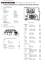
1.
Technical Specifications, Connections and
Chassis Overview
2
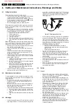
2.
Safety & Maintenance Instructions, Warnings
and Notes
4
3.
Directions for Use
6
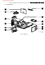
4.
Mechanical Instructions
17
5.
Service Modes, Error Codes and Faultfinding
21
6.
Block Diagram, Testpoints, and Overviews
Wiring Diagram
33
Block Diagram Supply and Deflection
34
Block Diagram Video
35
Block Diagram Audio
36
I
2
C-IC Overview
37
Supply Lines Overview
38
Testpoint Overview LSP & CRT/Auto SCAVEM 39
Testpoint Overview SSB
40
7.
Electrical Diagrams and PWB’s
Diagram CBA
Main Supply
(Diagram A1)
41
51-57
Stand-by Supply
(Diagram A2)
42
51-57
Line Deflection
(Diagram A3)
43
51-57
Frame Deflection & E/W Drive
(Diagram A4)
44
51-57
Rotation Circuitry
(Diagram A5)
45
51-57
Audio Amplifier
(Diagram A6)
46
51-57
Tuner SIMM connector (Female)(Diagram A8)
47
51-57
Receiver
(Diagram A9)
48
51-57
Front
(Diagram A10) 48
51-57
Inputs/Outputs
(Diagram A11) 49
51-57
Diversity Tables LSP
50
SIMM connector (Male)
(Diagram B1)
58
68-77
IF, I/O Videoprocessing
(Diagram B2)
59
68-77
PICNIC
(Diagram B3A) 60
68-77
Diversity Tables SSB
61
68-77
Falconic
(Diagram B3B) 62
68-77
Eagle
(Diagram B3C) 63
68-77
HOP
(Diagram B4)
64
68-77
OTC
(Diagram B5)
65
68-77
Audio Demodulator
(Diagram B6)
66
68-77
Anti Moiré
(Diagram B9)
67
68-77
Headphone Amplifier
(Diagram B10) 67
68-77
DW Panel: Multi PIP Contr.
(Diagram C1)
78
83-84
DW Panel: Tuner
(Diagram C2)
79
83-84
DW Panel: I/O Processing
(Diagram C3)
80
83-84
DW Panel: IF Video Sync
(Diagram C4)
81
83-84
DW Panel: V-chip Processor
(Diagram C5)
82
83-84
3D Comb Panel
(Diagram CO) 85
86-85
AC Power Switch Panel
(Diagram E)
87
88
CRT (Diagram
F1)
89
91-92
CRT/Auto Scavem Panel
(Diagram F2)
90
91-92
CRT 2
(Diagram F1)
93
95-96
CRT/Auto Scavem Panel 2
(Diagram F2)
94
95-96
DC Shift Panel
(Diagram G)
97
97
VDAF + 2nd Orders Panel
(Diagram I)
98
99
HD Jack Panel: Control
(Diagram N1)
100
103
HD Jack Panel: Inputs/Outputs (Diagram N2)
101
103
HD Jack Panel: Sync Slycer
(Diagram N3)
102
103
HD Jack Panel: Matrix
(Diagram N4)
102
103
Side I/O Panel
(Diagram O)
104
105
Top Control
(Diagram P)
106
106
Auto SCAVEM
(Diagram SC1) 107
108
8.
Alignments
109
9.
Circuit Description
117
Abbreviation List
138
IC Data Sheets
140
10 Spare Parts List
141
www.freeservicemanuals.info
Summary of Contents for EM5A NTSC
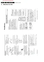
Page 6: ...Direction for Use EN 6 EM5A NTSC 3 3 Direction for Use www freeservicemanuals info ...
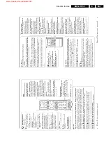
Page 7: ...Direction for Use EN 7 EM5A NTSC 3 www freeservicemanuals info ...
Page 8: ...Direction for Use EN 8 EM5A NTSC 3 www freeservicemanuals info ...
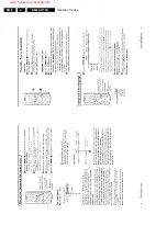
Page 9: ...Direction for Use EN 9 EM5A NTSC 3 www freeservicemanuals info ...
Page 10: ...Direction for Use EN 10 EM5A NTSC 3 www freeservicemanuals info ...
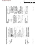
Page 11: ...Direction for Use EN 11 EM5A NTSC 3 www freeservicemanuals info ...
Page 12: ...Direction for Use EN 12 EM5A NTSC 3 www freeservicemanuals info ...
Page 13: ...Direction for Use EN 13 EM5A NTSC 3 www freeservicemanuals info ...
Page 14: ...Direction for Use EN 14 EM5A NTSC 3 www freeservicemanuals info ...
Page 15: ...Direction for Use EN 15 EM5A NTSC 3 www freeservicemanuals info ...
Page 16: ...Direction for Use EN 16 EM5A NTSC 3 www freeservicemanuals info ...


