background image

Published by WO 0364 Service PaCE

Printed in the Netherlands

Subject to modification

EN 3122 785 13130

©

Copyright 2003 Philips Consumer Electronics B.V. Eindhoven, The Netherlands.

All rights reserved. No part of this publication may be reproduced, stored in a 
retrieval system or transmitted, in any form or by any means, electronic, 
mechanical, photocopying, or otherwise without the prior permission of Philips.
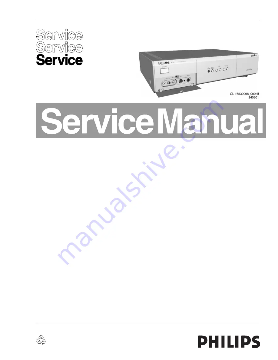
Colour Television

Chassis

F21RE

AB

Contents

Page

Contents

Page

1

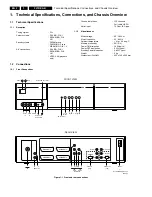
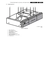
Technical Specifications, Connection Facilities, 
and Chassis Overview

2

2

Safety Instructions, Maintenance,

6

Warnings, and Notes

3

Directions for Use

7

4

Mechanical Instructions

26

5

Service  Modes, Error Codes, 

29

Faultfinding, and Repair Tips.

6

Block Diagrams
Block Diagram (Video)

37

Block Diagram (Audio + Supply)

38

Powerlines Overview

39

I

2

C IC’s Overview

40

Testpoint Overviews (AV + PS)

41

Testpoint Overviews (K + L + M)

42

Wiring Diagram

43

7

Electrical Diagrams and PWB lay-outs

Diagram PWB

AVI: Connections

(Diagram AV1) 44

52-54

AVI: HD-Matrix / Sync Remover (Diagram AV2) 45

46-48

AVI: Sync Processing

(Diagram AV3) 46

46-48

AVI: VGA / HD-Selection

(Diagram AV4) 47

46-48

AVI: Select. Supply

(Diagram AV5) 48

46-48

AVI: YPbPr-RGB Matrix

(Diagram AV6) 49

46-48

AVI: Video + RC-Selection

(Diagram AV7) 50

46-48

AVI: Audio + Control

(Diagram AV8) 51

46-48

2D Comb Filter Add-on

(Diagram CF)

55

55

Front Panel

(Diagram FP1) 56

57

SSB: Tuner, IF, Sourse Select  and Video 
Processing

(Diagram K1)

58

65-70

SSB: Input/Output

(Diagram K2)

59

65-70

SSB: Sound Processing

(Diagram K3)

60

65-70

SSB: Audio Dolby

(Diagram K4)

61

65-70

SSB: Video Geometry (Diagram K6)

62

65-70

SSB: TXT + Control

(Diagram K7)

63

65-70

SSB: Source Sel. (add to K1)

(Diagram K8)

64

65-70

Feature Box 7: Feature Box

(Diagram L1)

71

74-75

Feature Box 7: Eagle (NA)

(Diagram L2)

72

74-75

Feature Box 7: Falconic

(Diagram L3)

73

74-75

Power Supply

(Diagram PS)

76

77-78

SD Connector Panel

(Diagram SD)

79

80

8

Electrical Alignments

81

9

Circuit Descriptions

87

List of Abbreviations

99

IC-Data

101

10 Spare Parts List

107

11 Revision List

114

Summary of Contents for F21RE

Page 1: ...ectrical Diagrams and PWB lay outs Diagram PWB AVI Connections Diagram AV1 44 52 54 AVI HD Matrix Sync Remover Diagram AV2 45 46 48 AVI Sync Processing Diagram AV3 46 46 48 AVI VGA HD Selection Diagram AV4 47 46 48 AVI Output Select Supply Diagram AV5 48 46 48 AVI YPbPr RGB Matrix Diagram AV6 49 46 48 AVI Video RC Selection Diagram AV7 50 46 48 AVI Audio Control Diagram AV8 51 46 48 2D Comb Filter...

Page 2: ... voltage 95 264 Vac Mains frequency 50 60 Hz Ambient temperature 5 to 45 deg C Maximum humidity 90 R H Power ON dissipation 28 W typical Power OFF dissipation 0 2 W typical Standby Power dissipation 0 6 W Typical Weight 4 kg Dimensions WxHxD 435 x 100 x 330 mm 1 2 Connections 1 2 1 Front Connections Figure 1 1 Front and rear connections CL 16532098_004 eps 240901 IR Receiver Local Menu Volume Prog...

Page 3: ...FBL Ground 19 CVBS 1 V_pp 75 Ohm 20 CVBS 1 V_pp 75 Ohm 21 Shielding Ground EXT2 SCART In Out for VCR RGB CVBS SVHS Figure 1 3 SCART connector 1 Audio R 0 5 V_rms 1 kOhm 2 Audio R 0 5 V_rms 10 kOhm 3 Audio L 0 5 V_rms 1 kOhm 4 Audio Ground 5 Blue Ground 6 Audio L 0 5 V_rms 10 kOhm 7 Blue C 0 7 V_pp 75 Ohm 8 CVBS status 0 1 3 V INT 4 5 7 V EXT 16 9 9 5 12 V EXT 4 3 9 Green Ground 10 Easy Link P50 11...

Page 4: ...Blue 0 7 V_pp 75 Ohm 4 Data 2 n c 5 Test Ground 6 Red Ground 7 Green Ground 8 Blue Ground 9 n c 10 Ground 11 Data 0 n c 12 Data 1 n c 13 H sync 0 5 V 1 kOhm 14 V sync 0 5 V 1 kOhm 15 Data 3 n c Audio PC MAC In Cinch VGA1 Centre 1 Centre 0 5 V_rms 10 kOhm 2 Audio L 0 5 V_rms 10 kOhm 3 Audio R 0 5 V_rms 10 kOhm Audio Monitor Out Cinch VGA2 RC in 1 RC in 5 V 2 Audio L 0 5 V_rms 10 kOhm 3 Audio R 0 5 ...

Page 5: ...1 8 Panel position 1 Front I O Panel FP 2 Power Supply Panel PS 3 Double Window Panel if present 4 Feature Box FBX 5 Small Signal Panel SSP 6 Audio Video Interface Panel AVI 7 Scaler Panel if present 8 Standard Definition Connector Panel SD 9 3D Comb Panel C CL 26532054_008 eps 150502 2 6 8 7 4 3 9 5 1 ...

Page 6: ...llograms with regard to the chassis ground symbol or hot ground symbol The direct voltages and oscillograms shown in the diagrams are indicative Measure them in the Service Default Mode see chapter 5 with a colour bar signal and stereo sound L 3 kHz R 1 kHz unless stated otherwise and picture carrier at 61 25 MHz NTSC Where necessary measure the oscillograms and direct voltages with symbol and wit...

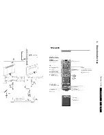
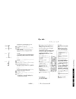
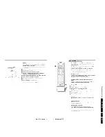
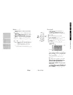
Page 7: ...Directions for Use EN 7 F21RE AB 3 3 Directions for Use ...

Page 8: ...Directions for Use EN 8 F21RE AB 3 ...

Page 9: ...Directions for Use EN 9 F21RE AB 3 ...

Page 10: ...Directions for Use EN 10 F21RE AB 3 ...

Page 11: ...Directions for Use EN 11 F21RE AB 3 ...

Page 12: ...Directions for Use EN 12 F21RE AB 3 ...

Page 13: ...Directions for Use EN 13 F21RE AB 3 ...

Page 14: ...Directions for Use EN 14 F21RE AB 3 ...

Page 15: ...Directions for Use EN 15 F21RE AB 3 ...

Page 16: ...Directions for Use EN 16 F21RE AB 3 ...

Page 17: ...Directions for Use EN 17 F21RE AB 3 ...

Page 18: ...Directions for Use EN 18 F21RE AB 3 ...

Page 19: ...Directions for Use EN 19 F21RE AB 3 ...

Page 20: ...Directions for Use EN 20 F21RE AB 3 ...

Page 21: ...Directions for Use EN 21 F21RE AB 3 ...

Page 22: ...Directions for Use EN 22 F21RE AB 3 ...

Page 23: ...Directions for Use EN 23 F21RE AB 3 ...

Page 24: ...Directions for Use EN 24 F21RE AB 3 ...

Page 25: ......

Page 26: ... 3 Double Window Panel if present 4 Feature Box 5 Small Signal Panel 6 Audio Video Interface 7 Down Scaler panel if present 8 High Definition panel 9 3D Comb panel US version only 4 2 Service Positions and Panel Removal 4 2 1 Front I O Panel Figure 4 3 Front cover removal Remove the front cover plate 1 Pull the lugs A on top bottom and both sides of the receiver box slightly aside 2 Pull the front...

Page 27: ... 3 Lead the removed cable in a favourable position and connect this cable again 4 2 4 Feature Box module Figure 4 7 Service position Feature Box panel FBX 1 Pull the clamps aside 1 and lift the Feature box module 2 2 Disconnect the cables and take out the module 3 Remove the shielding of the module de solder the fixation lugs 4 Remove the Feature Box panel from the module 5 Connect the cables and ...

Page 28: ...ht service position 2 To remove this panel pull it firmly out of its connectors mounted on the Audio Video Interface Note Be sure to keep track of the two copper grounding clips they can be lost very easily or they can cause short circuiting when falling into the receiver box 4 2 8 HD SD High Standard Definition Panel Figure 4 10 Removal of the HD SD connector panel There is no service position de...

Page 29: ... also measured on the connectors 5 2 Service Modes Service Default Mode SDM and Service Alignment Mode SAM offer several features for the service technician while the Customer Service Mode CSM is used for communication between the servicer and the customer There is also the option of using ComPair a hardware interface between a computer see requirements and the FTV chassis It offers the ability of...

Page 30: ...VICE OPTIONS In this sub menu the options can be set The quickest method to do this is through HW option number entry STORE OPTIONS Service options must be stored here Note Without storing no changes made to the options will be recorded The servicer must remember to store all changes before exiting SAM for those changes to take effect FUNCTIONAL TEST Activate this test by pressing the OK key on th...

Page 31: ...turation as set by the customer The parameter can vary from 0 minimum to 100 maximum Colour parameters can be changed by using the CURSOR LEFT and CURSOR RIGHT keys on the remote control transmitter after pressing the menu button and navigating to picture and setting colour HUE Gives the last status of the colour saturation as set by the customer The parameter can vary from 50 minimum to 50 maximu...

Page 32: ...fo This can be Off 4 6 8 10 12 14 or 16 years LOCK AFTER Gives the status info This can be Off Time e g 18 45 CATEGORY LOCK Gives the status info This can be Off Movies News Shows Sports Children Music or Culture PROGRAM CATEGORY Gives the status info This can be Off Movies News Shows Sports Children Music or Culture SW CODE 1 This code is only for Development Do not use it SW CODE 2 This code is ...

Page 33: ...the microprocessor is working and all repair information is directly available When ComPair is installed together with the Force electronic manual of the chassis being serviced schematics and PWBs are only a mouse click away 5 4 2 Specifications ComPair consists of a Windows based faultfinding program and an interface box between PC and the product The ComPair interface box is connected to the PC ...

Page 34: ...to the right 5 5 1 How to Read the Error Buffer It is possible to read out the error buffer in three ways On the screen while in Service Alignment Mode SAM If there is a picture this is the easiest way to read the error buffer In the SAM main menu the last 10 error codes which have occurred are displayed The most recently detected error code is displayed on the left side Examples 003 000 000 000 0...

Page 35: ...power supply of the device is missing FBX and or Tuner circuitry protection If one of these circuits does not respond for more than 1 second Error Device Description Defective item Diagram Defective module indication 2 ST24E32 or M24C32 Non volatile memory IC7008 K7 Control 3 SAA580x OTC2 5 microprocessor TXT IC7003 K7 Control 5 UV1316 Tuner U1102 K1 Tuner 10 TEA6415 I O source select video IC7208...

Page 36: ... the DST simulation mode or through the HW intervention of connector 0356 on the SSP pins 2 and 3 The set will now operate in SDM Then short pins 1 and 2 to enter SAM Via navigation in the SAM menu and selecting you must follow the this route Service Options Miscellaneous Stand alone Toggle No to Yes and store this change this means that a bit is changed in the NVM Now the Receiver box can operate...

Page 37: ...N6 IN8 IN7 IN5 IN1 OUT3 17 6 8 10 13 14 17 11 5 1 5 8 4 3 2 6 3 7 4 R G B 8 FBL 18 13 14 2 4 OUT4 OUT1 OUT2 IN2 7208 TEA6415CD TR IN8 IN7 IN1 IN5 IN4 IN6 IN3 OUT3 OUT4 OUT5 OUT6 OUT1 OUT2 16 9 DET FRONT DET F433 F434 F439 F641 F621 F601 F432 F431 F430 0399 1 2 3 4 5 6 7 8 9 10 11 F437 F770 F771 F702 F703 F438 F772 F773 F436 F435 F704 F705 10 9 12 13 7 8 14 1 2 3 4 Y VA OUT Y AV SYNC U VA OUT V VA ...

Page 38: ...IO AV8 AV5 AV7 AV8 AV8 K8 K6 AV5 F815 AV5 K7 AV4 AV5 AV4 AV5 AV5 AV8 AV6 K1 K6 CL 36532013_014 eps 020403 8 9 6 7 4 5 3 1 2 8 9 6 7 4 5 3 2 1 0328 0328 0344 11 11 10 10 3 1 11 10 4 7740 C 7749 7751 5 3 15 10 2 1 9 7740 B RC OUT RC MON 8VF 9 0303 2 1 TDX RXD 0355 1 3 89 90 5V2 FB 5V2 5VSTB 8V6 33V STANDBY 16V 5V2 FB 5V2 5VSTB 8V6 33V STANDBY 16V 0310 0310 1 2 3 4 5 6 7 8 9 1 2 3 4 5 6 7 8 9 0308 03...

Page 39: ...POWER ON POWER ON 5VSTB 5VSTBY 5VSTB 5VSTBY 8V6 5VSTB 5VSTBY 8VVA 8VT 5710 8VVA 5V 5VSTBY 33V 5VSTBY 5VSTB 5VSTBY 5VSTBA 3200 7V7 1101 T4A 6104 6105 1001 0300 T2 5A 95 264V 5003 6000 6000 GBU4J F042 F044 F052 F054 F056 F069 4 5 5202 4 7200 TNY256 2 3 6010 3 REF 7011 TL431 7002 TCET1103 8 1 1 4 3 2 0307 1 2 3 4 5 6 7 8 9 10 11 0308 3 9 10 11 0308 8VF 5VSTB 5VSTB 5VSTB 5VSTBY 2 3 4 6 7 8 2 3 6 5 4 P...

Page 40: ...IA COMPAIR TOOL VIA SET IN THE ERRORBUFFER FOLLOWING ERRORS CAN OCCUR CL 36532013_016 eps 020403 5 6 VIDEO SELECTION AV7 3722 2 3723 4 7710 TEA6415CD TR ELECTRONIC SWITCH ERR 30 K8 VGA HD SELECTION SOURCE SELECTION AV4 0371 3 4 0371 3 4 NOTE 1 ERR 65 2 ST24E32 NVM Non Volatile memory IC7008 K7 3 SAA5800 OTC2 5 microprocessor IC7003 K7 15 TDA9320 HIP I O video processing IC7501 K1 20 TDA9330 HOP vi...

Page 41: ...6 7011 4 1 8 5 F069 7202 4 1 8 5 7203 4 1 2 3 5200 5 6 10 1 2 7000 0306 5 3 F601 F621 F641 9 7 F660 F661 11 F670 0301 1 3 2 13 14 F440 F441 F442 F444 F445 F011 F013 F072 F008 0341 3 F740 F071 F012 F067 F444 F445 3580 F580 3579 3578 F579 F578 F052 F054 F056 5 0306 7 6 F032 F038 F042 F044 3 0307 11 8 7 USE LEAD AS HOT MEASURE GROUND USE HEATSINK AS COLD MEASURE GROUND 2 3 F460 2V div DC 20µs div F46...

Page 42: ...v DC 10µs div S8 EW 3 7300 S6 Frame 6 7300 0 1V div DC 5ms div S4 HFB 13 7300 1V div DC 10µs div I12 SIF Pin5 7501 0 2V div DC 5µs div I13 I2S DSP IN 5 7751 1V div DC 5µs div I14 I2S CL 7 7751 1V div DC 5µs div I15 I2S WS 6 7751 1V div DC 10µs div I1 1V4 DC I7 B7502 1V div DC 10µs div A25 SC2 L 50 7751 1V div DC 0 5ms div A24 SC2 R 51 7751 1V div DC 0 5ms div A7 ssp 0 5V div 0 2ms div A8 ssp 0 5V ...

Page 43: ...16 9_ARFRONT RXDO C_FRONT GND NC G_HD CVBS_Y_AV2 XXX XXX GND HD VDPOS 8V6 SNDL_MAIN_OUT 33V GND RC_OUT 7 Fold pos 8055 3 Fold U_DS_ Fh XXX XXX GND EHT_INFO TXDO CVBS_Y_AV1 X X X SND_CENTER G N D V_AV_OUT STANDBY 7V7 H_VGA NC NC NC XXX FBL_YUV V_MON VGA INPUT pos 8061 5V2 5V2_FB GND GND AV panel pos 8062 9 Fold SDA XXX GND 5V2_FB SDA_S SCL_S VDNEG 8V6 FEAT_U FEAT_Y 8V6 PS panel IN_UI_G U NC NC HFB ...

Page 44: ...2 5V 5VSTB 16 9_EXT3 1FH EXT_SYNC_PRESENT FBL_HD GND HD2_SEL HD_BLANKN HD_CLAMPN SNDL_MAIN_OUT SNDR_FRONT SNDR_MAIN_OUT Y_HD1 Y_SCALER 7V7 CVBS_Y_EXT3 C_EXT3 C_SCALER FBL_YUV GND G_SD I2C_SCALER_ACTIVE POWER_ON RC_EXT RC_FRONT_MON_SEL RC_FRONT_SEL_N RC_MON R_SD SCL_S SDA_S SNDL_FRONT R_HD_VGA SYNC_TRISTATE_MON VD V_HD_VGA 5VSTB 5VSTBA 5VSTBY 8V6 8VVA 50HZ_60HZ B_SD CVBS_SCALER 8V6 8VS 8VV 8VVA 7V7...

Page 45: ...5 C4 AV3 I284 C10 I285 D10 I286 D10 I297 F10 I298 G10 0V 0V 0V 0V 0V 0V AV6 AV6 AV6 AV6 AV6 0V AV4 AV4 AV4 AV3 AV3 AV3 6 AV3 4 1 1 AV6 1 1 1 1 1 1 0V 0V 0V 0V 0V 0V 0V 0V 0V 0V 0V 0V 0V 0V 0V 0V 0V 0V 0V 0V 2275 B8 2280 F13 2281 C10 2282 D10 0V 0V 0V 0V 0V 0V 0V 0V 0V 0V 0V 0V 0V 0V 0V 0V 0V 0V 0V 0V 0V 0V 1 1 1 6 7 8 9 10 11 12 13 A B 0V 0V 3271 G7 F276 I263 F277 F283 F269 I229 I231 BC847B 7273 I...

Page 46: ...72 IO44 73 IO45 78 IO46 79 IO47 80 IO48 81 IO49 82 IO5 13 IO50 83 IO51 86 IO52 38 IO24 39 IO25 41 IO26 43 IO27 44 IO29 47 IO3 10 IO30 48 IO31 49 IO32 51 IO33 59 IO34 60 IO35 62 IO36 63 IO37 64 IO38 65 IO39 8 IO10 21 IO11 22 IO12 23 IO13 26 IO14 27 IO15 28 IO16 29 IO17 30 IO18 31 IO19 32 IO2 9 IO20 33 IO21 36 IO22 37 IO23 57 GNDINT1 6 GNDINT10 104 GNDINT11 123 GNDINT12 129 GNDINT13 139 GNDINT2 15 G...

Page 47: ...3427 C6 3429 C6 3431 C6 3432 B10 3433 C10 3434 C10 3435 C10 0V 1V2 0V 0V 0V 5V1 0V 0V 0V 1V2 0V 1V2 0V 1V2 0V 1V2 0V 5V1 0V 0V 0V CONNECTOR NC 6441 G2 6442 G2 6444 I2 6445 I2 6450 F7 HD TRISTATE FROM TO BUFFER TO OUTPUT SUPPLY RES F436 F412 3445 8VV 600R 5400 7435 1K F442 3440 75R I451 2421 2u2 2450 100n 8VV 6 E 10 S 16 Vdd 7 Vee 8 Vss 2 Y0 1 Y1 Z 15 7400 B 74HC4053D I440 5V F409 74HC4053D 7400 A ...

Page 48: ...I592 E8 I593 F8 I594 G12 I595 G12 I596 E12 I597 F12 I598 F13 I599 E12 I544 F5 I545 E10 I546 E10 I547 F10 I549 F9 I550 A10 I551 G11 I552 A9 I553 B9 I554 B9 I577 E7 I578 E8 I579 E8 I580 D4 I581 F6 I582 F7 I584 H10 I585 H12 I586 I11 I587 I12 AV8 AV7 AV7 AV8 AV7 AV8 AV4 AV4 AV4 AV4 AV4 AV4 AV4 AV340 1 9 G H I 0303 B14 0306 H2 0307 G4 0310 G6 0315 H10 0340 A1 0355 F14 1512 G8 AV8 AV8 AV8 8V8 0V1 5V2 5V...

Page 49: ...6 2628 C9 2642 C6 2648 E9 2655 A1 2656 A2 2657 H3 2665 B3 0V 2670 I9 2671 G6 3 4 5 6 C HD CONNECTOR 3648 D9 3649 D8 3650 D8 3651 D8 3655 H3 3656 I3 3657 H3 3V2 0V 0V 0V 0V 0V 4V9 4V3 0V 4V9 0V 4V3 0V 4V9 0V 4V3 0V 0V1 4V4 3636 D4 3637 D3 2677 G6 1 2 3 4 5 6 10 11 12 13 1 2 I641 3602 100R 3642 100R I642 I602 F679 1K 3630 3650 2K2 BC847B 7635 I674 3606 1K2 3637 10K 3673 100R 22u 2622 7623 BC847B 10K...

Page 50: ... AV8 RC SELECTION AV8 AV8 AV5 AV8 AV8 AV8 AV8 AV3 6 AV3 AV3 AV3 AV3 AV3 AV4 AV4 AV4 AV4 AV5 AV5 AV3 4 8 AV3 4 8 AV8 AV6 8 AV5 SOURCE 3721 D4 3722 E5 3723 E5 3724 E6 3725 E6 3726 E9 3727 C9 3728 C9 3729 B9 3730 E8 3732 E6 3733 E6 3709 D3 3710 B4 3711 A3 3712 C8 3713 B3 3714 B7 3715 C3 3716 B5 3717 D3 3718 B5 3719 D4 3720 E7 3743 I10 SUPPLY AV309 0341 7751 PDTC124EU I756 I739 100K 3714 3757 22R E 6 ...

Page 51: ... H8 I866 H9 I867 H9 I868 G9 I869 H10 I870 G10 I871 H10 I872 H11 I875 I3 I876 I4 I880 D10 I881 C10 I882 C10 I889 E14 AV3 4 7 AV3 4 7 I O EXPANDER AV7 AUDIO_L 0313 B E1 A B C D E F G H I 0302 A C1 0302 B D1 0302 C H1 0305 A1 0313 A E1 10u 2815 0V 0V 0V 0V 0V 0V AV313 2812 22u I863 0313 B 5 2 F897 2844 22u I857 I848 F806 F825 F805 3861 10K I862 47K 3862 5VSTBA BC857B 7862 22u 2841 I864 F808 I854 3807...

Page 52: ...52 F21RE AB 7 Circuit Diagrams and PWB Layouts Layout AV Panel Top Side CL 26532118_009 eps 221002 3122 123 60092 ...

Page 53: ...94 B2 2400 D2 2420 C4 2421 C3 2423 C4 2425 C3 2427 C4 2429 C3 2431 C4 2450 A2 2451 A2 2460 A2 2510 A4 2511 A4 2512 B4 2513 A4 2514 D2 2515 A1 2520 C4 2521 C4 2522 A4 2523 C4 2524 A4 2525 C4 2526 B4 2527 C4 2528 A3 2529 C4 2530 A3 2531 C4 2532 B3 2534 A3 2536 A3 2538 B3 2542 B3 2545 A2 2546 A2 2550 F4 2551 F4 2570 B3 2571 A1 2575 F4 2585 A1 2587 A1 2588 A1 2601 F1 2607 F1 2608 F1 2610 E1 2622 F2 26...

Page 54: ...54 F21RE AB 7 Circuit Diagrams and PWB Layouts Layout AV Panel Bottom Side CL 26532118_010 eps 221002 3122 123 60092 ...

Page 55: ...3 F008 E8 I06 D2 I07 C4 I08 C3 0002 C8 0003 A8 1001 A7 Y CVBS IN 3002 C5 FOR RES Flying wire to clamp pulse SSP FTV1 9 only FTV 1 9 ONLY 1 RES 3003 D3 3999 E1 F004 7001 BC847B F003 F002 100n 2003 1K 3004 10 11 12 13 14 2 3 4 5 6 7 8 9 4 5 6 7 8 9 DSM2002 14 PB 0003 1 0002 DSM2002 14 PB 1 10 11 12 13 14 2 3 4002 F011 F008 F009 I08 3003 1001 1 100K 3002 3000 47K I01 3999 1K I07 F006 F007 F005 4000 F...

Page 56: ... A7 I142 A7 0V7 0V 5V3 CH 3058 E3 3060 D8 F106 B4 3062 D8 3063 D9 3065 E8 3066 E8 F111 B6 F112 D6 FP308 4V9 5V1 F107 B4 F108 C4 8V8 0V1 I106 C3 6041 B6 6046 C6 3044 3K3 I147 3058 47K 2050 100n 3057 10K 100u 2020 I130 F100 8VF 5VSTB 3 4 5VSTBY 120R 3017 0305 5 6 1 2 I137 3053 2K2 1 2 6070 BZM55 C33 6072 BZM55 C33 0302 3 F118 3052 3K9 8VF I150 BZM55 C33 6073 3062 3K3 I172 I157 8VF 1010 330p 2060 F11...

Page 57: ...05 A4 2040 B5 2048 B6 2050 B7 2055 A3 2056 A3 2057 A4 2060 B7 2061 B7 2065 B6 2066 B7 2072 B4 2075 B5 3001 A5 3008 B2 3009 B2 3010 B1 3011 B1 3012 B1 3013 B1 3014 B1 3015 B1 3016 B2 3017 B2 3018 A7 3019 B7 3025 A4 3026 A4 3027 A4 3028 A4 3029 A4 3030 A6 3039 B6 3040 B5 3041 B5 3042 B5 3043 B6 3044 A6 3045 A6 3046 B6 3047 B6 3048 B6 3049 B6 3050 B6 3051 B6 3052 A6 3053 A6 3055 A3 3057 B7 3058 B6 30...

Page 58: ...6106 I138 I139 4K7 3135 100K 3521 V2d 2503 100n F130 F144 5V 16V I101 180R 3138 I120 I122 I121 2561 47u 10u 2121 BC847B 3545 470R 7102 I115 10u 2572 4804 BA792 6103 5V 2K2 3111 5K6 3113 3116 5K6 1 2 3 4 6 7 8 820R 3590 5108 7KM F121 V3c 2788 4n7 100n 2555 I5 8 9 2105 1n5 0310 1 2 3 4 5 6 7 220n 2102 100n 2501 100R 3530 3110 3142 1K 3155 220R 2K2 7101 2556 100n 2536 100n BC847B 3560 470R 18p 2525 V...

Page 59: ...2 BZX284 C6V8 I308 2215 330p 150R 3258 I320 I321 F331 F314 1200 A YKC21 2675 4 1 3215 75R F313 F312 1K 3220 I301 6R8 3225 1K 3271 3826 150R F342 2205 10u 39R 3208 100R 3228 2240 100p 2209 330p 7203 BC557B 6236 BZX284 C10 BZX284 C10 6221 BZX284 C10 6214 I318 I309 F340 I324 3A 4A 5A 6A 7A 8A 9A BZX284 C6V8 6218 1A 10A 11A 12A 13A 14A 15A 16A 17A 18A 19A 2A 20A 21A 1201 A 6231 BZX284 C10 100p 2210 75...

Page 60: ...7V7 2754 F3 2755 F3 1 2 3 4 0V 2804 F2 9 10 0V K3 29 2759 G3 3753 G1 2781 E9 2778 E8 2779 E8 7V3 7V3 0V4 13 14 1 2 3 4 5 6 7 2783 470n 3787 22K 6K8 F417 22K 3752 3780 10K 3768 7V7 7V7 I425 18M432 1751 HC 49 U 7V7 5DB F401 2759 470p 2752 47p 3755 100R 4811 4810 I443 3778 33K 1R 3899 6K8 I420 3754 5DB 4721 I403 7V7 I408 F416 5DB 33K 3776 I435 LM833DT 7758 B 5 6 7 8 4 4806 7V7 2809 1n 2869 220u I421 ...

Page 61: ...0 22n 2833 I501 3825 56K 100R 3819 GND DIG I506 I507 I503 2828 10n 2817 10n 2834 F501 2851 2816 100u I510 A15a 10n 2813 43 3817 100K 22 VDDD5V2 34 VDDD5V3 42 VREFAD 75 VREFDA 15 VSS OSC 61 VSSA1 74 VSSA2 13 49 VSSD3V1 50 VSSD3V2 51 VSSD3V3 VSSD3V4 54 VSSD3V5 55 VSSD3V6 56 VSSD5V1 23 VSSD5V2 35 VSSD5V3 65 SRCO L 72 SRCO R 71 SRCOUT L 79 SRCOUT R 78 TSCAN 60 TUNER MPX 80 VDACN1 77 VDACN2 3 VDACP1 76...

Page 62: ...RES 75 4V I603 D9 I604 D10 I605 E11 I606 E8 I607 E11 I608 E9 I609 F3 RES F643 C2 F644 A5 F645 B5 I629 B5 I630 B5 I631 B5 I602 D9 K7 108 78 0V BC857B 7418 I619 H7 I620 D2 I621 H7 I622 G10 F632 F2 RES 20 XTALO 21 YIN 28 F1K RI1 30 RI2 35 RO 40 SCL 10 SCO 9 SDA 11 UIN 27 VD 23 VDOA 1 VDOB 2 VIN 26 VP1 17 VP2 39 VSC 15 XTALI 3 FBCSO 29 FLASH 5 GI1 31 GI2 36 GND1 6 GND2 19 GO 41 HD 24 HFB 13 HOUT 8 HSE...

Page 63: ...063 4K7 F231 470R 3005 A 1 8 3 6 5V2 3V3 STANDBY C3 100R 3098 D 4 5 3055 C 10R 100R 3092 A 1 8 7015 BC857B F220 10K 3035 7216 BC847B 3V3 STANDBY 3043 4K7 2026 100n 1 2 3 4 5 6 7 8 9 2 7 100R 3094 C 3 6 0341 470R 3004 D 4 5 100R 3094 B 27K I219 F232 3045 6u8 5002 100n 4020 3034 10K 2010 2 3 5V2 PLVA2650A 6026 0356 1 PLVA2650A 6019 5V STBY 2005 100n 2009 100n 47p 2042 2039 220p PDTA114ET 7012 10R 30...

Page 64: ...70 220n 220n 2250 F873 4616 4736 V11 I834 2862 4216 6K8 3884 220n 2258 BC857B 7207 I813 I812 V10 V12 V13 3873 10K F830 F819 F865 6750 MCL4148 F866 100n 2433 220n F823 3286 100K 2853 2863 F874 4R7 3437 4206 100n 2438 F829 4 5 6 7 8 9 F846 VCC1 33V 0362 1 2 3 3 IN3 1 IN4 11 IN5 5 IN6 8 IN7 6 IN8 13 OUT1 14 OUT2 17 OUT3 18 OUT4 15 OUT5 16 OUT6 4 SCL 2 SDA 7 SUB 9 TEA6415CD TR 7208 GND1 19 GND2 12 10 ...

Page 65: ...283 D4 3284 D5 3285 D5 3286 C5 3287 C5 3288 D4 3289 D5 3290 D5 3291 C5 3292 C5 3293 C5 3294 C5 3295 C5 3296 C5 3297 C5 3298 C4 3299 C4 3300 A3 3302 A5 3303 A4 3304 A4 3307 A4 3308 A4 3309 A4 3310 A5 3311 A4 3312 A4 3313 A5 3314 A4 3315 A5 3316 A5 3317 A4 3318 A4 3320 A5 3321 A5 3322 A5 3324 A5 3325 A5 3326 A5 3330 A5 3331 A5 3332 A5 3334 A5 3340 A5 3341 A5 3342 A5 3344 A5 3345 A5 3350 A5 3351 A5 3...

Page 66: ...66 F21RE AB 7 Circuit Diagrams and PWB Layouts Layout Small Signal Board Part 1 Top Side CL 36532030_01a eps 020403 ...

Page 67: ...Circuit Diagrams and PWB Layouts 67 F21RE AB 7 Layout Small Signal Board Part 2 Top Side CL 36532030_01b eps 020403 ...

Page 68: ... F3 3207 F3 3208 F2 3209 F3 3210 F3 3211 F3 3212 F2 3213 F3 3215 F3 3216 F3 3218 F3 3219 F3 3220 F2 3221 F1 3222 F1 3223 F1 3224 F1 3225 F2 3227 F2 3230 F1 3231 F2 3232 F1 3233 F4 3235 F1 3236 F1 3240 F1 3241 F1 3242 F1 3243 F1 3244 F1 3245 F1 3246 F1 3250 F2 3256 F3 3257 F4 3258 F4 3272 F4 3280 F4 3290 D1 3300 A3 3306 A1 3323 A1 3343 A1 3413 A1 3414 A1 3421 A3 3422 A1 3434 A3 3437 B1 3438 A1 3439...

Page 69: ...Circuit Diagrams and PWB Layouts 69 F21RE AB 7 Layout Small Signal Board Part 1 Bottom Side CL 36532030_02a eps 020403 ...

Page 70: ...70 F21RE AB 7 Circuit Diagrams and PWB Layouts Layout Small Signal Board Part 2 Bottom Side CL 36532030_02b eps 020403 ...

Page 71: ...DO15 60 DO16 61 DO17 74 DO20 73 DO21 71 DO22 70 DO23 69 DO24 68 DO25 66 DO26 65 DO27 31 IE1 95 IE2 85 MODE1 41 MODE2 42 MODE3 1 DI15 20 DI16 19 DI17 97 DI20 98 DI21 99 DI22 2 DI23 4 DI24 5 DI25 6 DI26 7 DI27 52 DO10 53 DO11 55 DO12 56 DO13 57 DO14 58 MS81V04160 7714 29 DI10 28 DI11 27 DI12 24 DI13 22 DI14 21 2722 100p 3724 680R F101 2725 10u 1K 3999 4K7 3758 4732 2750 100n F218 2777 100n F150 F217...

Page 72: ... 2921 2902 100n 3780 22R 120R 3848 100n 2898 2885 100n 2858 100n F215 3836 75R 560R 3849 2p2 2918 4740 F205 100n 2829 390R 3838 100n 2865 100u 2909 100n 2810 3831 680R BFS20 7731 3830 560R PMBT2369 7740 2901 100n 2856 100n 100n 2893 2867 2833 100n 100n 2904 100n 78 VSS17 87 VSS18 91 VSS19 9 VSS2 93 VSS20 10 VSS3 16 VSS4 17 VSS5 23 VSS6 33 VSS7 35 VSS8 39 VSS9 32 WE1 94 WE2 VCC2 14 VCC3 15 VCC4 34 ...

Page 73: ... YD1 118 117 YD2 116 YD3 115 YD4 114 YD5 112 YD6 111 YD7 122 YE0 123 YE1 124 YE2 125 YE3 126 YE4 127 YE5 128 YE6 52 YA7 159 YB0 YB1 158 157 YB2 156 YB3 155 YB4 154 YB5 152 YB6 151 YB7 2 YC0 3 YC1 4 YC2 5 YC3 6 YC4 7 YC5 8 YC6 135 VSS E2 78 VSS F2 59 VSS FL 81 VSS G1 99 VSS G2 143 VSS K 28 VSS S 146 WE B 106 WE D 45 YA0 46 YA1 47 YA2 48 YA3 49 YA4 50 YA5 51 YA6 23 VSS 2 55 VSS 3 58 VSS 4 100 VSS 5 ...

Page 74: ...3 C2 3704 C2 3705 C2 3706 C2 3707 C2 3708 C2 3709 C5 3710 C4 3711 C4 3713 C3 3715 C3 3716 C3 3718 C3 3719 C3 3721 C3 3722 C4 3723 C4 3726 C4 3728 C4 3729 C2 3730 C2 3731 C2 3732 C2 3733 C2 3734 C2 3735 C2 3737 A1 3739 A1 3740 C3 3742 C3 3743 C3 3745 C3 3752 C1 3753 C2 3758 C2 3764 B2 3767 A3 3774 A3 3780 A5 3782 A3 3783 A3 3786 B4 3787 C1 3788 C1 3789 C1 3790 C1 3791 C1 3792 C1 3793 C1 3794 C1 379...

Page 75: ...886 B2 2888 B2 2896 A1 2898 B2 2901 C2 2902 C2 2903 C2 2904 C2 2905 C2 2925 C2 2929 B4 3714 C3 3717 C3 3720 C3 3724 C3 3725 C2 3727 C2 3741 C3 3744 C3 3759 C4 3760 C3 3762 B2 3763 B3 3765 B4 3766 A4 3773 A4 3781 A4 3784 C4 3803 C2 3804 C2 3805 C1 3811 C2 3812 C2 3813 B2 3820 C2 3826 C2 3827 C2 3828 C2 3842 C2 3843 B2 3851 B2 3852 C2 3856 B1 3861 B4 3862 B4 3864 B3 3870 B2 3871 B2 3872 B3 4702 C4 4...

Page 76: ...2 D9 8 2054 B3 2101 B9 1400 A11 2000 B4 2001 B2 12 309V 308V 9 8 9 10 11 4V4 4V4 5V4 5V4 0V 0V 5V4 5V4 5V3 5V4 4V8 0V2 7V6 0V 9V2 0V4 0V5 A B C D E 347V 0V 0V 2V5 2V5 28V5 313V 309V 2V5 12V8 12V 0V 0V 0V 9V1 0V2 5V3 0V 9V0 149V 0V 0V 0V 0V 2V5 0V 2V6 0V 0V 1 2006 B6 2007 C5 2008 C7 5V4 5V4 5V2 0V 0V7 0V 0V15 0V6 0V7 0V 4V9 0V2 8V8 0V5 3V3 149V 0V 309V 0V 149V 0V 1V0 377V 1V2 13 14 308V 313V 249V 2...

Page 77: ...5005 C8 5101 A10 5102 B12 5103 C13 6202 A5 6203 A5 6204 A4 6310 A8 6401 A9 6402 A9 7000 B5 2002 B1 2003 B4 2004 A1 2005 C7 2006 C6 2007 B6 2008 C6 2202 A4 2203 B7 2207 A5 2311 A8 2313 A12 3000 A1 3001 A2 5104 A12 5200 A7 5201 A5 5202 A5 5300 All 5301 A8 6000 B4 7001 C5 7002 B9 7200 A5 7203 A7 2011 C6 2018 D5 2023 C4 2024 C4 2025 A6 2030 B9 2051 B9 3002 A2 3003 B2 3005 D3 3010 B7 3011 B5 3012 C6 30...

Page 78: ...3 A10 6204 All 6310 A7 6401 A6 6402 A6 7000 B10 7001 C10 7002 B6 7011 A4 7101 B1 7200 A10 7202 A6 7203 A8 7401 A4 7402 A3 F001 C14 F002 C14 F003 A13 F004 A13 F005 B11 F006 C8 F007 C11 F008 D8 F009 B12 F010 C12 F011 C7 F012 C11 F013 B10 F014 B10 F015 C9 F016 B6 F017 B6 F018 B6 F019 B5 F020 B5 F021 D4 F022 C2 F023 B4 F024 A5 F025 B4 F026 B3 F027 A7 F028 A1 F029 C1 F030 D1 F031 D2 F032 D1 F033 C1 F03...

Page 79: ...60 C A1 0361 A C1 0361 B C1 1001 A2 1002 A2 1003 A2 1004 B2 1005 B2 1006 B2 1007 C2 1008 C2 AV305 2 3006 C5 3007 C3 3008 C5 3009 C4 3010 C5 3011 C3 3012 C5 2 3 4 5 6 7 8 A 3009 1K 6001 BZM55 C33 75R 3003 6009 BZM55 C33 3002 75R BZM55 C33 6008 6006 BZM55 C33 6005 BZM55 C33 BZM55 C33 6004 BZM55 C33 6007 100p 2010 1004 2006 100p 3007 33K 33K 3011 1016 1009 1019 1013 1007 1005 1K 3005 1012 3 4 1003 03...

Page 80: ...80 F21RE AB 7 Circuit Diagrams and PWB Layouts Layout SD Connector Top Side Layout SD Connector Bottom Side CL 16532023_041 eps 200901 CL 16532023_042 eps 200901 Pe ...

Page 81: ...wnwards see figure SSP topview 4 Align the coil upwards untill under and overshoot arise at the black white and white black transitions in the video signal see figure Waveform sound trap alignment 5 Align the coil downwards again untill above mentioned under and overshoot just disappears Figure 8 1 SSP top view Figure 8 2 Waveform sound trap alignment 8 3 Software Alignments Notes Alignments are s...

Page 82: ...TTERN When this pattern is switched on the set will display a picture that slowly changes from black to white and vice versa Use this pattern to check the functionality of the circuitry behind the FBX and the FBX function itself You can also use this pattern as a picture generator for the Flat TV plasma monitor for example for checking cell defects interpretation of the ADC DAC converters etc Impo...

Page 83: ...a the mains switch the EAROM is then read again 8 4 2 Dealer Options Select this sub menu to set the initialisation codes options of the set via text menu s Figure 8 3 Dealer options overview CL 36532021_014 eps 310303 Menu name Subjects Options Physically in set Yes Video mute active when there is no signal detected Picture Mute No Noise when there is no signal detected Yes TV starts up with lang...

Page 84: ... with 32î FM23 monitor when jumper settings on AVI panel are configured in 2 3 mode FM24 SL Receiver box can operate with 42î FM24 monitor when jumper settings on AVI panel are configured in 2 3 mode SL Speaker Less FM25 SL Receiver box can operate with 50î FM25 monitor when jumper settings on AVI panel are configured in 2 3 mode SL Speaker Less Monitor type Monitor FM26 SL Receiver box can operat...

Page 85: ...a 0 11 n a 0 12 EPG Item for EU 0 Off fixed 4096 On 13 EPG Type for EU 0 Off fixed 8192 On 14 n a 0 2 15 n a 0 Sum OB2 decimal 0 AV3 0 Off 1 On fixed 1 AV4 0 Off 2 On fixed 2 AV4 2fH 0 Off fixed 4 On 3 n a 0 4 Dual Screen 0 Off fixed 16 On 5 Scaler 0 Off fixed 32 On 6 EPG TXT DS for EU 0 Off fixed 64 On not for US 7 Aux Headphone 0 Off 128 On fixed 8 Aspect Ratio 0 4 3 not appl for FTV 256 16 9 fi...

Page 86: ...Preference 0 TOP 4096 FLOF 13 n a 0 14 n a 0 5 15 n a 0 Sum OB5 decimal 0 P50 DVD menu line 0 Off 1 On 1 Asia 0 Off 2 On 2 n a 0 3 n a 0 4 n a 0 5 n a 0 6 n a 0 7 n a 0 8 n a 0 9 n a 0 10 n a 0 11 n a 0 12 n a 0 13 n a 0 14 n a 0 6 15 n a 0 Sum OB6 decimal 0 n a 0 1 n a 0 2 n a 0 3 n a 0 4 n a 0 5 n a 0 6 n a 0 7 n a 0 8 n a 0 9 n a 0 10 n a 0 11 n a 0 12 n a 0 13 n a 0 14 n a 0 7 15 n a 0 Sum OB7...

Page 87: ...tage The task of the main supply is to deliver the supply voltages for the several electrical circuits in the Receiver box It is switched via a single pole relay which is powered from the 5VSTBY voltage and controlled via the POWER_ON and STANDBY signals The reason to choose for a separate standby supply instead of a single flyback supply which can be driven in standby mode like a MC44604 is the r...

Page 88: ...ther ICs are initialised Now the E box is working but the monitor is still not displaying a picture 4 The HOP switches on the PHI1 loop the software sets all the necessary video and audio parameters and enables them Start up sequence for an E box FM2x Monitor There are five different power states in the E box Low Power Standby P 0 9 W The Main supply is not working Only the OTC I O Expanders on th...

Page 89: ...oltage isolation When the 5VSTBY output voltage rises the reference voltage on the TL431 will exceed 2 5 V and the current through this device and the optocoupler LED will increase By this method the optocoupler transistor will conduct more When this current at pin 4 of IC7200 exceeds 50 µA the MOSFET is switched off and the output voltage will drop When the current drops below 40 µA the MOSFET is...

Page 90: ...es the output pin 3 during the demagnetisation phase of transformer 5003 This is to prevent the FET from being switched on The info is taken from pin 8 of transformer 5003 and fed via R3015 and R3030 to pin 8 of IC7001 When the voltage on this pin drops below 65 mV the demagnetisation phase is completed and the FET can switch on Audio Plop The POWER_VALID circuit is designed to detect the disappea...

Page 91: ...D SND_SD SND_EXT3 YPBPR_SD SND_FRONT CVBS_YC_FRONT HV_MON RGB_MON SND_MON 5V2 8V6 16V 7V7 7V7 33V 5V2 8V6 RC SELECTION RC_MON RC_FRONT RC_EXT SND_CENTER HD PANEL FRONT PANEL SU POWER AVI PPLY RC_OUT SND_MAIN SND_SUB CVBS_YC_AV1 CVBS_YC_AV2 RGB_VC SND_SSP HV_VGA KEYBOARD IR_LED ON_OFF_LED POWER_ON POWER_ON STANDBY POWER_VALID 50HZ_60HZ KEYBOARD IR_LED ON_OFF_LED 5V2 8V6 STANDBY POWER_VALID 50HZ_60H...

Page 92: ...r the main picture is done with switch 7570 This switch is controlled via software with the HD_VGA_SELECT signal Note If the Receiver box has to function without the monitor e g in case of EPG data download the H and V pulses may not be fed to the monitor In this case switch 7570 will be put open with the SYNC_TRISATE_MON control signal SW controlled 9 3 4 AVI Audio Processing General The audio pa...

Page 93: ...7007 During a reset all I O pins are high When a RESET is generated the set is in Standby mode The 8V6 and the 5V2 are sensed by pins 105 and 106 If one of them is not present the Power supply is switched off The OTC will generate an error code to indicate what was wrong The horizontal HOSD PIP and vertical VD pulses are also fed to the OTC for stable OSD and CC To create good stable pulses these ...

Page 94: ...NT is derived from the RXDO signal with the aid of a one shot generator item 7545 In order to prevent the RXD line from connecting to ground a protection circuit is added This circuit puts the RXD buffer into tri state if the input is connected to ground for more than 100 ms Because the diversity is realized with jumpers connector 1519 there are no differences in panel stuffing for both versions T...

Page 95: ...functions Source selection Video IF demodulation Luminance chrominance and sync processing Inputs The set has a total of five external inputs AV1 5 The HIP has an integrated source selector which can handle 3 CVBS inputs 2 Y C inputs 2 RGB inputs The HIP detects whether the input is Y C or CVBS and decides what to do There are two inputs pins 39 and 40 for detection of the RGB status The other sta...

Page 96: ... the digital YUV YUV_FEAT signals from the PICNIC pins 12 14 and 15 enter the TOPIC This IC has the following functions Luminance Transient Improvement LTI Peaking Colour transients CTI and colour enhancement TOPIC The digital YUV signals from the PICNIC go via a passive output filter to the TOPIC and then to the HOP PICNIC Diagram L1 The PICNIC has the following functions ADC DAC Interlaced to pr...

Page 97: ...ifference is now 3 MHz This means that the picture for DVD is much better For this extra bandwidth an extra field memory is used IC7640 Improved motion detection Natural Motion This set utilizes AB A B scanning a new sample for Natural Motion The FALCONIC has an extra advantage for motion detection the maximum number of pixels that can be followed in AB A B scanning is higher This produces a more ...

Page 98: ... to connector 0340 which goes to the AV interface 9 4 6 SSP Audio processing Introduction The sound processing is distributed between the Flat Monitor amplifier and the Receiver Box processing The sound processing in the Receiver Box is completely done by the MSP 3410D demodulation for Europe and AP including NICAM or MSP 3440G demodulation for US LatAm Taiwan this IC also covers Korean stereo The...

Page 99: ...and the setting of the AutoTV button is limited to OFF ON Independent of Active Control is OFF MIN MED MAX Dependent of colour enhancement setting in picture menu and smart picture mode 9 7 Abbreviation list ADC Analogue to Digital Converter AM Amplitude Modulation AP Asia Pacific ATSC Advance Television Systems Committee AV External Audio Video AVI Audio and Video Interface B G Monochrome TV syst...

Page 100: ...Remote Control system 5 the signal from the remote control receiver RGB Red Green and Blue RGBHV Red Green Blue Horizontal sync and Vertical sync ROM Read Only Memory RXD Receive Data UART SCART Syndicat des Constructeurs d Appareils Radiorecepteurs et Televisieurs SCAVIO Scaler Control Audio Video Input and Output SCL Serial CLock I2C SD Standard Definition SDA Serial DAta I2C SDRAM Synchronous D...

Page 101: ...nput sources on 6 outputs Each output can be switched on only one of each input On each input an alignment of the lowest level of the signal is made bottom of synch top for CVBS or black level for RGB signals Each nominal gain between any input and output is 6 5dB For D2MAC or Chroma signal the align ment is switched off by forcing with an external resistor bridge 5 VDC on the input Each input can...

Page 102: ...IN BETWEEN ANY INPUT AND OUT PUT 55dB CROSSTALK AT 5MHz FULLY ESD PROTECTED DESCRIPTION The main function of the TEA6415C is to switch 8 video input sources on the 6 outputs Each output can be switched to only one of the inputs whereas but any same input may be con nected to several outputs All the switching possibilities arecontrolled through the I2 C bus DIP20 Plastic Package ORDER CODE TEA6415C...

Page 103: ...LLATOR PLUS CONTROL H V DIVIDER FILTER TUNING NTSC DECODER 14 22 24 18 17 MATRIX U V SIGNALS SATURATION CONTROL 8 1 6 20 21 LUMINANCE DELAY LINE AMPLIFIER 19 7 2 PULSE SHAPER 10 reference 4 PH1LF 9 DEC DIG 11 V P1 12 3 GND1 23 V P2 GND2 5 DEC BG CVBS CHROMA CVBS Y switch DEC FT PLL XTAL HUE SSC DEM SW SAT V U Y VOUT CLAMP HOUT TDA8315T 1 2 3 4 5 6 7 8 9 10 11 12 24 23 22 21 20 19 18 17 16 15 14 13...

Page 104: ...9 19 SAA4992 Internal Block Diagram SAA4992 FALCONIC BST test YA TEST TDI TCK TMS TDO SPM MOTION ESTIMATOR ESM TPM UPCONVERSION DEINTERLACER COMPRESS PIX PEAK DECOMPR DNR VERT PEAKING VERT ZOOM FM3 FM2 YB YC YD YF YE YG RIGHT MPRAM LEFT MPRAM SEQUENCER SNERT CONTROL Interface sn_rst sn_da sn_cl TRST clk32 VEC VEC mux mux ...

Page 105: ...68 69 70 71 72 73 74 75 76 77 78 79 80 vss_b2 YB0 YB1 YB2 YB3 YB4 YB5 vdd_b YB6 YB7 UVB0 UVB1 UVB2 UVB3 we_b vss_b1 n c vss_8 vdd_8 vddo4 n c n c vdd_7 vss_7 n c vss_e2 re_e UVE3 UVE2 UVE1 UVE0 YE7 YE6 YE5 YE4 YE3 YE2 YE1 YE0 vss_e1 vss_d2 YD0 YD1 YD2 YD3 YD4 YD5 vdd_d YD6 YD7 UVD0 UVD1 UVD2 UVD3 we_d vss_d1 vss_6 vdd_6 vdd_03 vdd_5 vss_5 vss_g2 UVG0 UVG1 UVG2 UVG3 UVG4 UVG5 UVG6 UVG7 vdd_g YG0 YG...

Page 106: ...w frequencies ADext3 low frequencies CF DECDIG PINNING BLOCK DIAGRAM SYMBOL PIN DESCRIPTION SC 1 sandcastle input NC 2 not connected ADEXT1 3 ADC input 1 ADEXT2 4 ADC input 2 ADEXT3 5 ADC input 3 YIN 6 luminance input ADR 7 address selection input UIN 8 colour U input VIN 9 colour V input TP 10 test pin SCL 11 serial clock input I2C bus NC 12 not connected NC 13 not connected SDA 14 serial data in...

Page 107: ...02 10µF 20 16V 3437 4822 051 20108 1Ω 5 0 1W 3440 4822 117 11927 75Ω 1 0 1W 3441 4822 117 11927 75Ω 1 0 1W 3442 4822 117 11927 75Ω 1 0 1W 3444 4822 117 11449 2k2 5 0 1W 0805 3445 4822 117 11449 2k2 5 0 1W 0805 3446 4822 117 11373 100Ω 1 0805 3447 4822 117 11373 100Ω 1 0805 3452 4822 117 10833 10k 1 0 1W 3453 4822 117 10833 10k 1 0 1W 3456 4822 117 10833 10k 1 0 1W 3462 4822 117 10833 10k 1 0 1W 35...

Page 108: ...2 130 11397 BAS316 6845 9322 149 10685 BZM55 C33 6846 9322 149 10685 BZM55 C33 6847 9322 149 10685 BZM55 C33 6848 9322 149 10685 BZM55 C33 6849 9322 149 10685 BZM55 C33 6850 9322 149 10685 BZM55 C33 6862 4822 130 11397 BAS316 6867 4822 130 11397 BAS316 6868 4822 130 11397 BAS316 6869 4822 130 11397 BAS316 6870 4822 130 11397 BAS316 6875 4822 130 11397 BAS316 6876 9322 149 10685 BZM55 C33 7450 5322...

Page 109: ...22 33891 3 3nF 10 63V 2116 4822 124 81044 470 F 20 6 3V 2117 4822 126 13482 470nF 80 20 16V 2118 5322 122 32967 5 6pF 10 63V 2119 5322 122 31863 330pF 5 63V 2120 4822 126 14076 220nF 25V 20 2121 4822 124 40248 10µF 20 63V 2125 4822 122 33177 10nF 20 50V 2126 4822 124 40433 47µF 20 25V 2127 4822 126 14076 220nF 25V 20 2202 5322 122 31863 330pF 5 63V 2203 5322 122 31863 330pF 5 63V 2204 2238 586 598...

Page 110: ...20Ω 1 0 1W 3137 4822 051 10102 1k 2 0 25W 3138 4822 117 11448 180Ω 1 0 1W 3139 4822 117 11139 1k5 1 0 1W 3140 4822 117 12955 2k7 1 0 1W 0805 3141 4822 051 30562 5k6 5 0 063W 0603 3142 4822 051 30102 1k 5 0 062W 3143 4822 051 30102 1k 5 0 062W 3145 4822 051 30391 390Ω 5 0 062W 3146 4822 051 20223 22k 5 0 1W 3147 4822 052 10109 10Ω 5 0 33W 3152 4822 051 20471 470Ω 5 0 1W 3153 4822 051 10102 1k 2 0 2...

Page 111: ...mper 0805 4111 4822 051 20008 Jumper 0805 4226 4822 051 20008 Jumper 0805 4227 4822 051 20008 Jumper 0805 4316 4822 051 20008 Jumper 0805 4402 4822 051 20008 Jumper 0805 4403 4822 051 20008 Jumper 0805 4410 4822 051 20008 Jumper 0805 4413 4822 051 20008 Jumper 0805 4414 4822 051 20008 Jumper 0805 4420 4822 051 20008 Jumper 0805 4423 4822 051 20008 Jumper 0805 4424 4822 051 20008 Jumper 0805 4426 4...

Page 112: ...100nF 80 20 50V 0603 2782 2238 586 59812 100nF 80 20 50V 0603 2783 2238 586 59812 100nF 80 20 50V 0603 2784 2238 586 59812 100nF 80 20 50V 0603 2785 2238 586 59812 100nF 80 20 50V 0603 2786 2238 586 59812 100nF 80 20 50V 0603 2787 2238 586 59812 100nF 80 20 50V 0603 2788 2238 586 59812 100nF 80 20 50V 0603 2789 2238 586 59812 100nF 80 20 50V 0603 2790 2238 586 59812 100nF 80 20 50V 0603 2791 2238 ...

Page 113: ...5k 1 0 1W 3034 4822 116 83933 15k 1 0 1W 3035 4822 117 10361 680Ω 1 0 1W 3036 4822 116 83933 15k 1 0 1W 3037 4822 051 20184 180k 5 0 1W 3038 4822 117 13577 330Ω 1 0805 1 25W 3039 4822 051 20223 22k 5 0 1W 3040 4822 117 11504 270Ω 1 0 1W 3041 4822 051 20182 1k8 5 0 1W 3042 4822 050 23309 33Ω 1 0 6W 3043 4822 050 21501 150Ω 1 0 6W 3044 4822 051 20392 3k9 5 0 1W 3101 4822 050 23302 3k3 1 0 6W 3102 48...

Page 114: ...Revision List EN 114 F21RE AB 11 11 Revision List First release ...

Reviews: