background image

Published by MW 0667 BG CD Customer Service

Printed in The Netherlands

Subject to modification

EN 3122 785 16400

©

Copyright 2006 Philips Consumer Electronics B.V. Eindhoven, The Netherlands.

All rights reserved. No part of this publication may be reproduced, stored in a 
retrieval system or transmitted, in any form or by any means, electronic, 
mechanical, photocopying, or otherwise without the prior permission of Philips.

Colour Television

Module

FHP PDP Repair Manual


FPF42C128135UA-52 (42” A4)

Contents

Page

1.

Technical Specifications

2

2.

Safety Instructions, Warnings, and Notes

5

3.

Directions for Use

6

4.

Mechanical Instructions

6

5.

Service Modes, Error Codes, and Fault Finding 10

6.

Block Diagrams, Test point Overview, and Wave 
Forms

27

7.

Circuit Diagrams and PWB Layouts

29

8.

Alignments

29

9.

Circuit Descriptions and Abbreviation List

30

10. Spare Parts List

33

11. Revision List

34

Summary of Contents for FPF42C128135UA-52

Page 1: ...c mechanical photocopying or otherwise without the prior permission of Philips Colour Television Module FHP PDP Repair Manual FPF42C128135UA 52 42 A4 Contents Page 1 Technical Specifications 2 2 Safety Instructions Warnings and Notes 5 3 Directions for Use 6 4 Mechanical Instructions 6 5 Service Modes Error Codes and Fault Finding 10 6 Block Diagrams Test point Overview and Wave Forms 27 7 Circuit...

Page 2: ... FPF42C128135UA 52 1 Resolution 1024 H x 1080 V pixels 1 pixel 1 R G B cells 2 Number of Cells 3072 H x 1080 V 3 Pixel Pitch 0 90 mm H x 0 485 mm V 4 Cell Pitch 0 30 mm H x 0 485 mm V 5 Display size 921 60 H x 523 8 mm V 6 Screen size Diagonal 42 7 Screen aspect 16 9 8 Dimensions 994 W x 587 H x 66 D mm 9 Weight About 16 kg 10 H sync V sync data 50 kHz H 50 60 70 Hz V LVDS Serial Number G_16400_00...

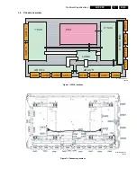
Page 3: ...1 3 Chassis overview Figure 1 5 PWB locations Figure 1 6 Connector positions 㪯㪝㪧㪚 㪯㪝㪧㪚 㪯㪝㪧㪚 㪯㪝㪧㪚 㪪㪛㪤㪄㪬 㪘㪙㪬㪪㪄㪣 㪰㪄㪪㪬㪪 㪘㪙㪬㪪㪄㪩 㪣㪦㪞㪠㪚 㪪㪛㪤㪄㪛 㪧㪪㪬 㪯㪄㪪㪬㪪 㪘㪛㪤㪈 㪘㪛㪤㪉 㪘㪛㪤㪊 㪘㪛㪤㪋 㪘㪛㪤㪌 㪘㪛㪤㪍 㪘㪛㪤㪎 㪘㪛㪤㪏 㪯㪄㪙㪬㪪㩷㩿㪯㪙㪙㪀 G_16400_005 eps 180706 G_16400_006 eps 270706 ...

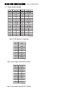
Page 4: ...al name 1 RA 2 GND LVDS 3 RA 4 SCL 5 RB 6 GND 7 RB 8 SDA 9 RC 10 GND LVDS 11 RC 12 CPUGO 13 RXCLKIN 14 PDPGO 15 RXCLKIN 16 IRQ 17 RD 18 PDWN 19 RD 20 GND LVDS 21 RE 22 GND 23 RE 24 GND 25 GND 26 GND 27 GND 28 GND 29 GND 30 GND G_16400_035 eps 280706 Pin No Symbol 1 Vcc 2 GND 3 Vpr2 4 GND 5 Vra 6 Vrs 7 VCEGO 8 VSAGO 9 PFCGO G_16400_036 eps 270706 Pin No Symbol 1 Va 2 N C 3 Vcc 4 GND 5 GND 6 GND 7 N...

Page 5: ...oduced by the screen pollutes the communication the set can be set in Stand by mode Then still the error messages can be retrieved 2 3 1 Notes on Safe Handling of the Plasma Display Notes to Follow During Service The work procedures shown with the Note indication are important for ensuring the safety of the product and the servicing work Be sure to follow these instructions Before starting the wor...

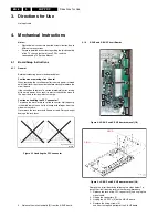
Page 6: ...l electric charge Caution on handling the FPC connector To release the black lock lever of the connector flip it up gently in the middle with the nail of the thumb or forefinger from the side with the cable Never pinch the lock lever with fingers or tools Doing so might damage the lock lever Figure 4 1 Handling the FPC connector 4 1 2 X SUS and X BUS Circuit Boards Figure 4 2 X BUS and X SUS board...

Page 7: ...2 3 Remove the fixing screws 3 4 Release the white stand offs 4 from the Y SUS board 5 Pull out the Y SUS board horizontally in this way unplugging the connectors 5 6 Remove the Y SUS board Make sure that you do not touch the heat sink when removing the Y SUS board Note Make sure the radiation plate is positioned correctly It is located underneath the upper SDM and the threaded bush should sit in ...

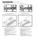
Page 8: ...e fixing it with the screws 4 1 5 ABUS R Circuit Board Figure 4 9 ABUS R board removal 1 2 Figure 4 10 ABUS R board removal 2 2 Remove the circuit board by following the steps below To install the circuit board reverse the removal procedure 1 Unplug the connector 1 2 Remove the screws 2 fixing the ADMs 3 Release the lock of the FPC connectors 3 and remove the ADM flexible board 4 Release the lock ...

Page 9: ... cables 3 Remove the screws 3 fixing the LOGIC board 4 Remove the LOGIC board 5 When installing the LOGIC board put the board in such a position that it is locked by the tabs 4 before fixing it with the screws 4 1 7 PSU Board Figure 4 13 PSU board removal Remove the circuit board by following the steps below To install the circuit board reverse the removal procedure 1 Unplug connectors 1 2 Remove ...

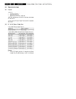
Page 10: ...ead out the error buffer 5 2 2 Error Code Overview Table 5 1 Error code table G_16400_018 eps 270706 Power Supply Logic Board CN06 CN01 I 2 C Compair Vpr 3 SDA GND SCL CN06 I2 C Compair 8 6 4 CN01 3k3 3k3 14 E_14580_024 eps 250304 Error code Detected by board Error description Suspected board s 21 X SUS Vxx power voltage is too high X SUS LOGIC 24 Vxx power voltage is too low X SUS LOGIC 25 Vex po...

Page 11: ...ot mentioned in 5 2 1 the workshop orders the necessary spare parts being boards at EuroService After receipt the workshop swaps the concerning board and makes the TV set complete by building in the PDP Afterwards the TV set is returned to the customer Figure 5 3 PDP flow chart End user contacts dealer because his plasma TV set is defective VIP workshop pays home visit to end user and swaps defect...

Page 12: ...ogic Board Exchange 1 and 2 must be used Display type Service code number FPF42C128135UA 52 9322 235 43682 Module description FHP code number Service code number X SUS board FPF33R XSS0041 9965 000 35647 Y SUS board FPF33R YSS0042 9965 000 35648 Logic board FPF33R LGC0061 9965 000 35646 A BUS Left FPF33R ABL0038 9965 000 35649 A BUS Right FPF33R ABR0039 9965 000 35650 X BUS board FPF33R XBU0035 99...

Page 13: ...SUS SDMs PDP Repair procedure Board Swap Vertical Line Vertical Bar Horizontal bar Check if Vcc 5V Vs 85V and Logic Board Exchange procedure Use of ComPair Copy data from the defective Logic board Restore data into the new board Ship Out Auto alignment procedure G_16400_025 eps 310706 Va 63V are present Check if there is a short circuit on boards ABUS L ABUS R or ADMs X BUS or XFPCs on PSU and boa...

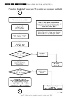
Page 14: ...he mains plug Remove the following power connections on X SUS CN23 PSU X SUS on X SUS CN26 X SUS ABUS R on X SUS CN32 X SUS Y SUS on ABUS R CN47 ABUS R ABUS L Problem Analysis Procedure The entire screen does not light Caution 1 never disconnect connectors or remove boards when the mains plug is connected Allow discharge of power supplies before disconnecting connectors All the boards are connecte...

Page 15: ...ard is defective PDP is defective On X BUS board CN61 pins 1 9 are shorted X SUS Y SUS 13 X SUS Y SUS Vu NC Vcc Vs Vs NC GND 1 Vs 12 11 10 9 8 7 6 CN22 4 3 2 5 NC GND NC Vs NC 10 X SUS PSU 2 5 GND GND Vcc NC GND Vs 1 Va 9 8 7 6 4 3 CN23 Vs NC Vs Y SUS X SUS Vcc NC Vx Vs Vs NC GND 1 Vs 13 12 11 10 9 8 7 6 CN32 4 3 2 5 NC GND NC Vs NC A2 A1 B1 B2 C1 C2 D1 D2 3 End of analysis G_16400_027 eps 310706 ...

Page 16: ... CN 55 CN 56 ADM is defective PDP is defective ABUS L board is defective N Y N ABUS R board CN42 pins 1 3 or CN42 pins 3 5 are shorted Remove ADM from the following connectors CN 43 CN 44 CN 45 CN 46 ABUS R board is defective N Y Replace the defective part ABUS L ABUS R ABUS L board CN52 pins 1 3 or CN52 pins 4 7 are shorted ABUS R board CN42 pins 1 3 or CN42 pins 3 5 are shorted ADM is defective ...

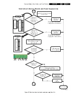
Page 17: ...ive Vcc starts but goes down in a few seconds Y N 1 When turning ON the PDP with PDP go refer to following procedure 1 Connect the special LVDS cable see paragraph Repair Tools 2 Supply power to the PSU On PSU board Vcc 5V Vs 85V exist Turn OFF AC power Connect SDM with CN34 and CN35 Give the PDP go signal 1 SDM or PDP is defective Turn OFF AC power Connect CN 26 X SUS Give the PDP go signal 1 PSU...

Page 18: ...cable LOGIC board ABUS R L board signal cable has abnormal appearance 1 Logic board is defective or ABUS R board is defective or Signal cable is defective or loose contact of CN02 LOGIC or CN41 ABUS R Left half of the panel does not light Y N Va 63V exists on RL41 resistor on ABUS L board Y N N Y Logic board is defective or ABUS L board is defective or Signal cable is defective or loose contact of...

Page 19: ... AC power Replace LOGIC board Give the PDP go signal 1 Normal LOGIC board is defective Y Turn OFF AC power Replace LOGIC ABUS L signal cable Give the PDP go signal 1 Normal Y Signal cable is defective N N Replace the defective parts Is vertical bar monochromatic 1 2 3 ADM is defective PDP is defective Y G_16400_031 eps 310706 1 When turning ON the PDP with PDP go refer to following procedure 1 Con...

Page 20: ...nal cables LOGIC ABUS R N Panel is defective PDP is defective Replace the defective parts Normal Y Signal cable is defective ADM is defective PDP is defective N 2 3 Turn OFF the main power Replace ABUS R board G_16400_032 eps 310706 1 When turning ON the PDP with PDP go refer to following procedure 1 Connect the special LVDS cable see paragraph Repair Tools 2 Supply power to the PSU between CN01 a...

Page 21: ...ive Y Turn OFF the main power Replace the X SUS board N Normal Y SUS board is defective PDP is defective Y N Replace the defective parts Turn OFF the main power Remove the X SUS board Put back the initial X SUS board Replace Y SUS board G_16400_033 eps 310706 1 When turning ON the PDP with PDP go refer to following procedure 1 Connect the special LVDS cable see paragraph Repair Tools 2 Supply powe...

Page 22: ...e information to a file This is optional but better safe than sorry Note If you close the window without saving all settings Logic Board Exchange 1 1 Copy NVM Data from defective Logic Board Remove the Small Signal Board 1 2 4 Set will go into protection or into stand by 5 Click the link in ComPair to open the Logic Board exchange window 6 Click the On button In the title bar the module type will ...

Page 23: ...the new board If successful the button Ship out will be enabled 6 Click button Ship out 7 Now a process of voltage feedback initialization and self adjustment starts This will take a few seconds When ready you can switch off the display 8 Disconnect ComPair and remove the service cable plug in the power cable at CN06 and the original LVDS cable at CN01 G_16400_020 eps 010806 Logic Board Exchange 2...

Page 24: ... 4 Vertical line Vertical line from the middle of effective scan area vertical line of different color Panel chassis Replace panel chassis 5 Bar width of 1 7 of horizontal size or in multiples of 1 7 is displayed Abnormal display Panel chassis ABUS L ABUS R LOGIC Above boards are connected 6 Vertical bar Bar width of 3 7 or 4 7 of the screen width is displayed Abnormal display vertical line of dif...

Page 25: ...entarily becomes brighter or darker Poor connector contact 13 Flicker The entire screen flickers continuously Poor connector contact CN2 3 21 31 Connector cable re connection or cable exchange 14 Luminance is abnormal Screen is too dark or too bright Out of specifications 15 Chrominance is abnormal Colors cannot be displayed correctly LOGIC board Replace Logic board following the Logic Board Excha...

Page 26: ... Only partial picture Unstabel picture Flickering flashing picture Lines across down image Inactive row s Inactive column s Missing colour s Other Pixel Defect s Dark dots Bright dots Qty of dots Mark Defect s Following defect symptoms are out of warranty R I A P E R L E N A P Symptoms Out of warranty Broken glass Scratch es on display Number of dark bright pixels within spec Burn in only for Plas...

Page 27: ...D M U S D M D SCAN CONTROLLER FRAME MEMORY DATA PROCESSOR OSC TIMING ROM γ comp OSC 80MH MPU OSC 10MHz Y SUS X SUS LOGIC Board Y SUS EVEN SW X SUS EVEN SW CN31 Y SUS ODD SW Y SCAN ODD SW X SUS ODD SW X SCAN ODD SW RGB GAIN DITHER ERR SUB FIELD PRC POS RESET SW POS NEG RESET SW MEMORY CONTROLLER ADM1 ADM4 ADM8 ADM7 ADM6 ADM5 ADM3 ADM2 LVDS 24MHz SIGNAL INPUT Vrs Vra Vrw Vrx D A V SYNC cont APC cont...

Page 28: ... DC CONVERTER Vxwgo Vcc 5V Vs 85V Va 63V Vw 190V Vu 55V POS NEG RESET SW Vcc 5V Vs 85V Va 63V Vcc 5V Vcc 5V Va 63V Va 63V CN32 CN22 CN42 CN52 CN36 CN26 ADM8 ADM7 ADM6 ADM5 ADM3 ADM2 ADM4 Vs 85V PFC Vs Va 5 3 3V Control PSU Vra Vcc MPU 380V PFCgo Vsago Vcego Vsago Vcego PFCgo 10A CN61 CPUgo PDPgo CN23 5V 63V AC100 240V DC DC CONVERTER XFVE Vxx VE 18V 20V 17V Vcc 5V DC DC CONVERTER YFVE Vy VE 18V 18...

Page 29: ...e Setting label shows the following messages Table 8 1 If the voltage adjustments Vs and Va on the Power Supply Unit must be performed depends on the version of the Power Supply Unit G_16400_034 eps 270706 Item Adjustment items Measurement point Adjustment value conditions 1 Vs voltage adjustment Pins 8 9 10 of CN23 on the X SUS board Voltage setting label indication value 1 2 Va voltage adjustmen...

Page 30: ...ontrol parameter memory Counts operating time number of hours Abnormal status memory 16 places 9 1 2 Function of X SUS Board DC DC power supply block Vcc 5V Ve 17V XFve 18V floating X Switching Block Switching during address period Switching during sustain period Switching during reset period Current Detector Block I_sx sustain current detection I_ax address current detection 9 1 3 Function of Y S...

Page 31: ...he Logic Board is standardised The power cable from the PSU to the Logic Board is standardised Item 42A1 42A2 42A3 42A4 Dimensions mm 994 x 585 x 66 994 x 585 x 66 994 x 587 x 66 994 x 587 x 66 Weight kg 16 16 16 16 Resolution h x v 1024 x 1024 1024 x 1024 1024 x 1024 1024 x 1080 Brightness cd m2 display load 1 standard 1 100 1 200 1 400 1 400 Contrast dark room 1000 1 1000 1 3000 1 3000 1 SDM U A...

Page 32: ...and X BUS A new connector type is used on ABUS L ABUS R and X BUS Figure 9 4 Layout 42A4 Differences with respect to 42A3 There are no differences in cable arrangements with respect to 42A3 G_16400_040 eps 310706 XFPC XFPC XFPC XFPC SDM U ABUS L Y SUS ABUS R LOGIC SDM D PSU X SUS ADM1 ADM2 ADM3 ADM4 ADM5 ADM6 ADM7 ADM8 X BUS XBB G_16400_041 eps 310706 XFPC XFPC XFPC XFPC SDM U ABUS L Y SUS ABUS R ...

Page 33: ... Each PC board and parts mounted in the PC boards PDP Plasma display panel abbreviated Probe A cable with contact finger that can transfer the status of the electric circuit to be measured to an oscilloscope Protection cover A cover made of aluminium to protect the PDP entirely during test ROM Memory that stores the drive sequence and other data SCAVIO Scaler Control Audio Video Output Input SDM S...

Page 34: ...als covered by this manual 11 1 Service Manual xxxx xxx xxxx 0 First release Display type Model CTN Chassis 12NC Manual 42 A4 42PF5331 10 LC4 41E AA 3122 785 16240 42PF5411 10 LC4 41E AA 3122 785 16240 42PF9531 79 BJ3 0A PA 3122 785 15980 42PF9531 93 BJ3 0A PA 3122 785 15980 42PF9531 98 BJ3 0A PA 3122 785 15980 42PF9631D 10 BJ3 0E PA 3122 785 15960 ...

Reviews: