background image

Published by RB 0262 Service PaCE

Printed in the Netherlands

Subject to modification

EN 3122 785 11650

©

Copyright 2002 Philips Consumer Electronics B.V. Eindhoven, The Netherlands.

All rights reserved. No part of this publication may be reproduced, stored in a 
retrieval system or transmitted, in any form or by any means, electronic, 
mechanical, photocopying, or otherwise without the prior permission of Philips.

Colour Television  

Chassis

L01H.1A

AA

CL 26532029_000.eps

010302

Contents

Page

Contents

Page

1.

Technical Specifications, Connections and 
Chassis Overview

2

2.

Safety & Maintenance Instructions, Warnings and 
Notes

4

3.

Directions for Use

5

4.

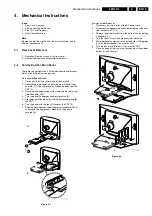
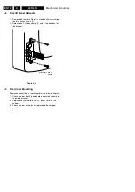
Mechanical Instructions

13

5.

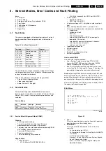
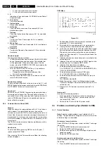
Service Modes, Error Codes and Faultfinding

15

6.

Block Diagram, Testpoints, I

2

C And Supply 

Voltage Overview
Block Diagram

19

Wiring Diagram

20

Testpoint Overview

21

I

2

C And Supply Voltage Overview

22

7.

Electrical Diagrams and PWB’s

Diagram PWB

Power Supply

(Diagram A1)

23

36-41

Line Deflection

(Diagram A2)

24

36-41

Frame Deflection

(Diagram A3)

25

36-41

Tuner IF

(Diagram A4)

26

36-41

Video IF and Sound IF

(Diagram A5)

27

36-41

Synchronization

(Diagram A6)

28

36-41

Control

(Diagram A7)

29

36-41

Audio Amplifier

(Diagram A8)

30

36-41

NICAM (Stereo/SAP) Decoder (Diagram A9)

31

36-41

Audio/Video Source Switching (Diagram A10) 32

36-41

Front I/O + Control, Headphone (Diagram A12) 33

36-41

Rear I/O Cinch

(Diagram A13) 34

36-41

Tilt and Rotation

(Diagram A15) 35

36-41

CRT

(Diagram B1)

42

44

SCAVEM

(Diagram B2)

43

44

Side AV

(Diagram E)

45

45

Side AV and Headphone

(Diagram E1)

46

46

EPS4B External Power Supply (Diagram F)

47

48

UIR/LS Module

(Diagram H)

49

51

Interface Panel

(Diagram J)

50

51

Front Interface & Control Panel (Diagram Q)

52

53

Front Interface

(Diagram Q1)

54

54

8.

Alignments

55

9.

Circuit Description 

60

List of Abbreviations

69

10 Spare Parts List

71

Summary of Contents for L01H.1A

Page 1: ...ing Diagram 20 Testpoint Overview 21 I2C And Supply Voltage Overview 22 7 Electrical Diagrams and PWB s Diagram PWB Power Supply Diagram A1 23 36 41 Line Deflection Diagram A2 24 36 41 Frame Deflection Diagram A3 25 36 41 Tuner IF Diagram A4 26 36 41 Video IF and Sound IF Diagram A5 27 36 41 Synchronization Diagram A6 28 36 41 Control Diagram A7 29 36 41 Audio Amplifier Diagram A8 30 36 41 NICAM S...

Page 2: ... G B H D K I SECAM B G D K K1 Sound systems FM stereo 2CS B G China Korea BTSC DBX NICAM B G D D K I BI NICAM B G D D K I A V connections NTSC 3 58 4 43 PAL 60 Channel selections 100 or 125 channels UVSH or full cable Aerial input 75 Ω IEC or F type 1 1 2 Miscellaneous Audio output 2 x 5 W with SAP 2 x 5 W 10 W subwoofer 2 x 5 W 10 W 2 x 3 W Mains voltage 90 276 V or 150 276 V Mains frequency 50 o...

Page 3: ... 5V 4 DATA OUT 5 GND 6 IR DATA 1 4 SPEAKER 2 SPEAKER PHONE JACK FOR BATHROOM SPEAKER CL 16532138_011 eps 221101 4 1 2 1 16 17 32 CL16532138_028 eps 171201 32 PIN SMART CARD CONNECTOR PIN 1 RESERVE 2 GROUND POWER 3 12V 4 GROUND IIC 5 IR DATA 6 POR 7 TV CLOCK 8 DATA IN 9 DATA OUT 10 5V 11 HORIZONTAL SYNC OUT 12 VERTICAL SYNC OUT 13 GROUND CVBS IN 14 SCL 15 SDA 16 RESERVE PIN 17 ANALOG BLUE IN 18 ANA...

Page 4: ...e levels for example in a kitchen the recommended interval is one year The maintenance inspection includes the following actions 1 Perform the general repair instruction noted above 2 Clean the power supply and deflection circuitry on the chassis 3 Clean the picture tube panel and the neck of the picture tube 2 3 Warnings In order to prevent damage to ICs and transistors avoid all high voltage fla...

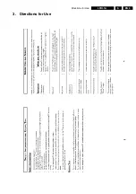
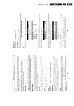
Page 5: ...Directions for Use EN 5 L01H 1A 3 3 Directions for Use ...

Page 6: ... for Use EN 6 L01H 1A 3 6 B AC K C ONNECTORS W ARNING R ISK OF ELECTRIC SHOCK DO NO T REMOVE THIS COVER D O NO T CONNECT TELEPHONE CABLE TO RJ11 CONNECT OR Smar t Card slot For Y models For R models For Z models ...

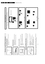
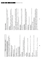
Page 7: ...Directions for Use EN 7 L01H 1A 3 ...

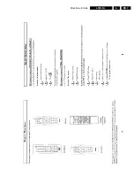
Page 8: ...Directions for Use EN 8 L01H 1A 3 ...

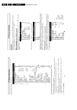
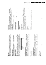
Page 9: ...Directions for Use EN 9 L01H 1A 3 ...

Page 10: ...Directions for Use EN 10 L01H 1A 3 ...

Page 11: ...Directions for Use EN 11 L01H 1A 3 ...

Page 12: ...Directions for Use EN 12 L01H 1A 3 Personal Notes ...

Page 13: ...g the cable from red connector 0201 4 Turn the panel 90 degrees counter clockwise 3 5 Flip the panel 90 degrees 4 with the components towards the CRT 6 Turn the panel with the rear I O towards the CRT 5 7 Slide the metal heatsink near the mains transformer 5520 underneath the right chassis bracket so the panel is secured 6 Figure 4 1 Main panel with bracket 1 Disconnect the strain relief of the AC...

Page 14: ...amps 2 and lift the board out of the bracket Figure 4 3 4 4 Rear Cover Mounting Before you mount the rear cover perform the following checks 1 Check whether the AC power cord is mounted correctly in its guiding brackets 2 Replace the strain relief of the AC power cord into the cabinet 3 Check whether all cables are replaced in their original position CL 06532012_004 eps 030200 ...

Page 15: ...inutes skip blank of non favourite presets channels auto store of personal presets auto user menu time out Operation hours counter Software version Option settings Error buffer reading and erasing Software alignments How to enter SDAM Use one of the following methods Use a System 7 remote control type T374AH RC transmitter RG4172BK and key in the code 062596 directly followed by the M menu button ...

Page 16: ...er Service Mode the following screen will appear CSM Menu Figure 5 2 1 Software identification of the main micro controller see paragraph 5 2 1 for an explanation 2 Error code buffer see paragraph 5 4 for more details Displays the last five errors of the error code buffer 3 In this line the Option Bytes OB are visible Each Option Byte is displayed as a decimal number between 0 and 255 The set may ...

Page 17: ... time the buffer was erased The buffer is written from left to right When an error occurs that is not yet in the error code buffer it is written at the left side and all other errors shift one position to the right 5 4 1 How to Read the Error Buffer Use one of the following methods On screen via the SDAM only if you have a picture Examples ERROR 0 0 0 0 0 No errors detected ERROR 6 0 0 0 0 Error c...

Page 18: ...ptoms are given followed by a repair tip Set is dead and makes hiccuping sound MainSupply is available Hiccuping stops when de soldering L5561 meaning that problem is in the MainSupply line No output voltages at LOT no horizontal deflection Reason line transistor TS7460 is defective Set is dead and makes no sound Check power supply IC7520 Result voltage at pins 1 3 4 5 and 6 are about 180 V and pi...

Page 19: ...TA IN CLOCK SCL 7901 AN7522N STEREO 7902 AN7523N MONO 6 2 L L 8 9 MONO AM MONO SOUND VOLUME MUTE A5 1 MAINAUX_FB ERR 7 7209 7210 FM RADIO PRE AMPL 0280 A2 4 L A3 10 R A4 12 R R L R 4 3 2 1 0278 3 2 1 0255 4 3 2 1 L L R R L L R R SIDE AV OR FRONT INTERFACE Q L L R R L L R R 0254 1 2 3 4 1246 Spk Spk 1 2 2 U2 4 1 5 0267 0246 1 2 3 4 5 1259 1259 VIDEO TO 0240 CONTROL A7 F TO 0228 EPS 4B 32 PIN SMART ...

Page 20: ...0259 5P 0251 4P 0239 3P 0246 5P 0229 3P 0242 10P 0211 2P 0212 2P 0214 5P 0255 4P 0215 3P 0215 3P 0211 2P 1259 9P 0259 5P 0251 4P 0219 6P 0280 4P 0217 6P 0242 7P 0227 6P 0236 3P 0227 6P 0217 4P 0228 5P 0240 7P 0237 4P 0255 4P 0251 3P 1246 1251 3P 3P 0254 5P 1259 9P 0259 5P EPS 4B PANEL TOP CONTROL TOP CONTROL FRONT INTERFACE PANEL F INTERFACE PANEL J T E E1 T1 Q1 Q UIR LS MODULE H OR SIDE AV 0254 5...

Page 21: ... div A9 500mV div DC 500us div A10 500mV div DC 500us div A11 1V div DC 200us div A11a 500mV div DC 2us div C1 1V div DC 500us div C2 C1 1V div DC 500us div F1 500mV div DC 5ms div F2 500mV div DC 5ms div F3 10V div DC 5ms div F4 5V div DC 5ms div I1 2V div DC 200us div I2 2V div DC 200us div I3 500mV div DC 10us div I4 20mV div DC 10us div L1 1V div DC 20us div L2 1V div DC 20us div L4 5V div DC ...

Page 22: ...NISATION A6 7200 D SYNC PROC 5241 8V 5V 5V 140 95V VLOT AUX 50V 8V 8V 8V 8VA TO 3248 7200 A VIDEO IF 9 5832 BTSC DECODER NICAM 2CS A9 VLOT AUX 5V REAR I O CINCH A13 A15 8V AUDIO VIDEO SOURCE SWITCHING A10 UIR LS H 7831 AUDIO DECODER 5833 5VA 8V 6V8 46 33 3455 3447 3446 3488 6467 6488 7482 7480 6486 6482 3450 3449 6481 3801 3625 7602 M24C08 EEPROM NVM 3624 3607 3606 3604 3603 6 5 72 71 68 7 ERR 9 E...

Page 23: ... I534 A5 I535 G11 I536 C10 I537 A11 I538 F11 I539 F11 I540 D9 I541 E9 I542 C9 I543 C2 I544 C3 I546 D5 12V 11V5 2n2 LE33CZ I548 C4 I549 C4 I550 D2 I551 D9 I552 C11 6 3V 10K 3530 7521 F502 2K2 3532 39K 3545 4 5 8 9 3506 1M5 10 11 12 13 14 15 16 17 18 2 3 5520 I524 2540 10n 6560 2n2 2501 2515 3564 2562 1n 6561 SB340 2528 1n I552 100n 2520 2561 3508 I511 7522 BC847B I525 1N4148 6566 3523 I507 2566 470...

Page 24: ... 5 6 BZX79 A6 23 5V2 0V 7 8 9 10 11 12 A B C D 2422 B4 2423 B4 2441 F9 2443 F11 2444 G9 2448 B9 2450 A5 2451 A6 A2 16 A5 16 RES LINE DEFLECTION 5V7 D 5V2 8V 8V 1 2 3 4 5 6 7 8 9 10 for Europe Only 0V 5V5 CU15 13V3 E W CORRECTION 8V9 A6 18 E F G H 0220 B3 0221 B7 1400 C5 2400 F4 2401 G5 2402 G4 2404 H6 2405 D3 2415 E3 2420 C4 2421 B4 F443 I445 F454 I467 47n 2443 I491 9462 5400 I404 1 4 I401 2415 G5...

Page 25: ...YES YES 2467 9463 9464 YES REGION TUBE Diversity Table A2 470n 2u2 2n2 2u2 15n 22n 15n 68n 330R 560n 68n 330R 33K 100K 1K 4R7 4R7 100R 10K 180R 15K 10K 8K2 10K 470R 2R2 1000u 02472 53201 02478 37021 LAL04 33U 02465 34901 LAL04 56u C39 BY228 24 YES YES YES 50V 2u2 470p 47u 560n 2u2 820p 15n 10n 15n 68n 470n 330R 33K 100K 1K 4R7 4R7 100R 10K 4R7 180R 820R 47K 15K 15K 10K 8K2 27K 1K 6R8 30531 02469 5...

Page 26: ...C4 F009 F4 F010 A5 Non FM Radi o LA NA AP 45 75 LNA UV1336A 0V 2006 B7 2007 B7 2008 C6 2009 C9 OF A7 13 A7 3 3004 C8 3005 C8 3006 E6 3007 D6 3008 D6 3009 D7 3010 D4 3011 D5 4001 D6 4002 F8 4003 E7 4004 E8 4005 E7 4006 E6 4011 F8 4012 G8 5001 B7 5002 C6 RES A5 24 A5 27 Non LNA 34V5 Mono LNA 5V 5003 F9 6001 B6 6002 C7 6003 C7 ITEM AP CH 38 9 38 0 D E F G 0265 A5 0283 C3 0285 B3 1000 B4 1002 D8 1003 ...

Page 27: ...B2 0266 E11 0276 D3 0297 D6 1200 E8 1201 E8 1202 F8 2201 D2 2202 C2 E F G H A B A4 27 CRT 2V5 2234 F7 2235 F9 2236 G8 2237 G9 2238 G7 2239 G7 C D E 3219 G3 3220 B4 3217 G6 2215 F2 A9 42 3211 F9 3210 E7 3209 D8 3208 E9 3207 C9 A4 29 0V 0V 2221 C2 2225 C8 2227 D11 2228 D11 2229 C11 3200 B9 3201 C6 F202 C6 F201 C6 A5 42 A4 28 100MHz A5 42 1V9 3V6 2203 D3 0V for M nas only 2V6 0V 3226 560R 1V7 FOR ITV...

Page 28: ...r 270K 270K 680K C 680K 680K 3250 8K2 SMD Jumper SMD Jumper SMD Jumper SMD Jumper 8K2 8K2 8K2 8K2 8K2 8K2 2244 680K 680K 680K 680K SMD Jumper 4K7 4K7 8K2 8K2 I248 100n 2250 2u2 I252 3247 220K I241 3242 27K I245 3248 33K 1M 3254 1n 4u7 2246 2243 2n2 2252 I243 S5 100K 3258 1n 2253 5242 10u I250 3256 1K S4 10u 5241 S3 100R 3251 3246 10K I244 I247 F241 I251 10M 3257 2247 I254 2241 1n5 I249 2245 220n 2...

Page 29: ...17 D3 0V 3V3 DATA OUT RES A8 6 Bass_panorama 0V A4 3 3V3 F607 E10 F608 B7 A12 4 F611 B10 F612 A5 F613 E3 F614 E4 I601 A9 I608 D8 I609 E7 I610 H3 I612 D4 I613 D4 I614 B6 I615 B4 I616 B5 I617 C5 4603 B8 RES SET WITH YUV F606 A10 EEPROM 3V2 A2 9 3610 Mono BG I DK M CH 8K2 4618 YES YES 3612 IF 38 9 8K2 8K2 BG DK M ITEM QSS AP IN IF 38 9 QSS AP IF 38 0 BG I DK M QSS 0240 2607 2609 2AVIn 1AVIn ITEM Non ...

Page 30: ... 6901 B6 6903 B4 7901 B7 7902 D7 7943 F4 9901 C9 9902 C9 9903 B4 9904 B4 F901 C3 F902 C4 F903 D3 F904 D4 F903 Jumper RES AUDIO_AMPLIFIER 2 X 5W VOICE A7 15 8 Ohm 2 X 1W 8 Ohm A12 70 I904 C6 I905 D5 I906 D6 I907 D4 I908 E6 I909 B5 I910 C8 I911 G3 I912 D10 I948 F4 I949 F4 2901 Mono 1W 2946 1u A3 F909 2907 9901 1 2 3 4 5 F905 2903 1u 0246 3948 100K 3949 33K 9903 I949 2902 3921 330K I948 F901 A2 0275 ...

Page 31: ...2843 A7 2844 D4 2845 D4 2846 H2 2847 D4 2848 D4 5V RES 5V 1V5 A10 51 0V 2V5 5V 3V 3V 2V6 1V5 0V 0V 1V8 RES A7 13 MSP34X5G QSS DBX GS 2 3 4 A7 8 3V1 3V A B C D E F 27p 15p 56p RES 2859 G3 2860 F3 2887 C10 5 6 7 8 9 10 11 0V NICAM 2CS BTSC STEREO SAP DECODER 2860 3834 3843 4835 5835 1u RES RES RES RES 100R RES RES RES RES 150p RES 2K2 Jmp 12u 33p 47p 180p 2K2 RES RES RES RES RES RES RES RES RES RES ...

Page 32: ...60 A9 48 1V8 ITEM Mono 5V A13 32 A13 52 3809 5V8 0V 5V 0V 1V6 5V 0V 1V6 0V 1V6 0V 5V8 A9 50 2V4 2V5 3V8 2x Rear Video In x Jumper x To Micronas BTSC UOC 6V From Micronas 2u2 A5 37 A14 55 A14 60 A14 52 A12 31 A9 47 3V8 A12 58 A13 59 A9 49 A12 53 From MicroP 0V 2V3 A7 12 5V8 A13 54 A13 55 2V4 From Front Rear I O A14 63 2u2 2u2 A14 57 2V4 From Micronas A13 61 A14 62 A14 61 6V A14 32 ITEM 1V7 Stereo S...

Page 33: ...1602 B10 1603 B9 1606 B8 2181 B4 I693 D10 V FRONT IO FRONT CONTROL HEADPHONE FOR ITV ONLY A12 8 A C D E F G A B C D E 0218 A 7 8 9 4692 2183 1 2 3 4 5 2694 F683 0214 2182 1182 0218 C 1 2 3 F692 I185 6181 AudioSupplyGnd_FB 2693 1606 1600 SKQNAB 3981 0219 1 2 3 4 5 6 AudioSupplyGnd_FB 3686 1K5 F693 1602 10u 2983 22p 2181 I981 I693 0286 1183 4693 I986 2691 10u 3982 3184 4 5 6 9181 2695 0218 B 3694 4K...

Page 34: ...3123 G4 3124 G5 3125 G4 3126 G5 3131 B9 3132 B8 3133 C9 3134 C8 3135 D8 3136 D8 3137 D8 3138 D8 3141 G8 F109 G3 F110 B9 RES RES 2u2 75R 100R 75R 100R SET WITH YUV RES x x FOR ITV TO 0227 OF Y 0269 I101 B6 I102 B6 TO 0242 OF A7 2 L FOR PIP TO 0219 OF V U L U L TO 0229 OF A7 75 A11 60 FOR SETS WITH 9 3P CINCH PIP SET 3159 E2 4101 C3 I103 C6 I104 C6 I105 D6 I106 D6 I107 E5 I108 E5 I109 E5 I110 F5 I11...

Page 35: ... D6 I171 C2 I172 C2 I173 C3 I174 D3 A8 74 TO TILT ROTATION TDA8941P A B C D E B C D E 3171 C2 3173 C2 3174 C3 7000 C4 F171 C6 ROTATION COIL 1 2 3 4 5 6 1 2 3 4 5 6 I173 I174 I171 I172 SVR 6 VCC 1 7000 GND 8 IN 3 IN 5 MODE 4 OUT 2 OUT 7 0268 1 2 3 68K 3173 2172 220p F171 2171 100p 3174 68K 3171 120K Tilt VlotAux 13V VlotAux 13V F172 CL 16532101_014 eps 230801 Personal Notes ...

Page 36: ...36 L01H 1A 7 Schematics and PWB s Layout Large Signal Panel Top View CL 16532053_005 eps 050601 ...

Page 37: ...arge Signal Panel Mapping Top View CL 16532053_05m eps 100701 Layout Large Signal Panel Overview Bottom View CL 16532053_006 eps 100701 Part 1 CL 16532053_06a eps Part 3 CL 16532053_06c eps Part 4 CL 16532053_06d eps Part 2 CL 16532053_06b eps ...

Page 38: ...38 L01H 1A 7 Schematics and PWB s Layout Large Signal Panel Part 1 Bottom View Part 1 CL 16532044_06a eps 240801 ...

Page 39: ...Schematics and PWB s 39 L01H 1A 7 Layout Large Signal Panel Part 2 Bottom View Part 2 CL 16532053_06b eps 310501 ...

Page 40: ...40 L01H 1A 7 Schematics and PWB s Layout Large Signal Panel Part 3 Bottom View CL 16532053_06c eps 040601 Part 3 ...

Page 41: ...Schematics and PWB s 41 L01H 1A 7 Layout Large Signal Panel Part 4 Bottom View Part 4 CL 16530153_06d eps 050601 ...

Page 42: ...10 11 A B C D E 2V6 10 11 1 2 3 6333 B5 6335 B5 7330 B3 9341 B3 9342 B3 C F300 B6 E F VG2 F10 0165 A8 I302 B4 I303 C4 I304 C5 I305 B5 I306 C5 I307 E7 I308 E7 I309 F3 I310 E6 I311 E2 I312 D3 I313 D6 197V 0V 2346 F6 3331 C5 3332 C5 0244 E2 0245 D2 0254 A B7 0255 B7 0256 A B7 2330 B4 TO 2341 F5 OF CRT B2 69 1 3349 B3 3350 C2 3351 C2 3352 C3 3353 D2 3354 D2 3355 D3 5342 C6 5343 B2 5344 C2 5345 D2 6331...

Page 43: ...369 D4 2371 E4 2372 C5 2 1 2 3 4 5 6 3389 E8 8 9 10 11 1 3374 D9 3375 D10 3376 D6 3377 D7 3378 E9 3379 D4 3382 E7 3383 E6 7 8 9 10 11 A B C D E F 3369 C7 B1 67 3371 C4 3370 C6 2373 E5 7V6 2374 2374 E6 2375 D10 3360 A8 3361 B3 3362 B4 3363 C9 3364 C9 3368 C6 D E F 0278 D11 2360 B9 7 10K 3369 2K7 3368 330R 3370 3383 470R 2373 I340 F334 3376 470R 3375 F330 3379 4K7 3360 2369 2371 10R 3391 2364 3390 1...

Page 44: ... 3389 A2 5342 A2 5343 A1 5344 A1 5345 A1 5360 A2 5361 A2 5362 A2 6331 A1 6333 A1 6335 A1 6360 A1 7330 A1 7360 A1 7362 A2 7363 A1 7365 A2 7366 A2 7367 A1 9311 A1 9341 A1 9342 A1 9343 A1 9361 A2 9363 A2 9364 A2 9365 A1 9366 A2 CL 16532053_011 eps 240801 Layout CRT Panel Bottom View CL 16532053_011 eps 110501 2342 A1 2344 A1 2364 A1 2367 A1 2368 A2 2369 A1 2371 A1 2372 A1 2373 A1 2374 A1 2375 A2 3347...

Page 45: ... 4 A B C D E A B C D E 0250 A B1 9155 0250 B C1 0250 C A1 0251 B4 0252 B1 0253 A4 0261 D4 1152 A2 1153 C2 1154 B2 2171 C3 2172 B3 2173 B2 2174 C2 2175 B1 3150 C3 3151 C3 3152 B3 3153 B3 3155 A3 9152 5010 B3 6161 A3 9152 B2 9153 B3 9155 B3 9153 330p 2175 330p 2171 330p 2172 5010 0261 1 2 3 4 5 6 2174 2173 0252 1 2 3 4 3 0253 1 2 3 0251 1 2 1 2 3 75R 3155 1152 0250 C 0250 B 4 5 6 6161 BZX79 C6V8 115...

Page 46: ...E A B C SG06 0252 B2 0253 A5 0254 D2 0255 D5 0261 C5 2171 C4 2172 B4 2173 B3 2174 C3 2176 E3 2177 E2 2178 E3 2179 D2 3150 C3 3151 C3 3152 B3 3153 B3 3155 A3 3156 D3 3157 E3 6161 A3 9153 B3 9155 B4 SG02 A3 SG03 C3 SG04 B3 SG06 E3 SG07 E3 4 1 2 3 4 0255 1 2 3 0251 1 2 3 0252 0253 1 2 3 3157 9155 3156 0254 1 2 3 4 5 2174 2177 100u 2176 100u 2179 3 4 5 6 7 8 9 2178 2172 330p 0232 1 2 2173 1 2 3 4 5 6 ...

Page 47: ...0UF 25V 5A 40V 5A 40V 43R 3A 100V 3A 100V KA278R12 KA278R05 470UF 10V 22R 47UF 16V 0 1UF 50V 0 1UF 50V 250mA 200V 470PF 250V TLP721 10A 30V 22R 0 01UF 1KV UU9 8 22MH UU9 8 22MH 1A 250V 0 1UF 275VAC 1A 600V 1 5M 1 2W 7 5M 33UF 450V 5W 400V 2K 3 3K 10K 0 22UF 50V AN1431 100R 1 4W 510R 0 1UF 50V 470UF 10V 470UF 25V 470UF 10V DR6 8 16UH 1A 100V 1A 100V RH 3 5 0 8 9 220UF 10V RH 3 5 0 8 9 RH 3 5 0 8 9 ...

Page 48: ...1 C7 B3 C11 B3 C12 D2 C20 C1 C21 C1 C23 A3 C24 B3 C25 B3 C26 B2 C27 B2 C28 D3 C29 B2 C35 A3 C36 A2 C38 B2 C39 A2 CR1 B3 CR2 B3 CR3 B4 CR4 B4 D1 D3 D2 C2 D3 B2 D4 A1 D5 A2 F1 E3 G1 A2 IC1 C2 IC2 B2 IC3 B1 IC4 A4 IC5 A3 J1 A4 L1 D4 L2 D2 L6 C2 L7 A2 L8 A2 L9 B2 L10 B1 R1 C3 R2 C2 R3 C2 R4 D4 R11 C1 R12 C2 R13 B3 R13 B3 R14 B1 R16 B1 R23 B4 R25 B2 R26 B2 R27 B3 R28 B3 R29 B3 ZD1 D3 ZD2 C3 ...

Page 49: ...470R Q1 BC847B Q7 BC847B U3 HEF4053 Vdd Vss Vee En 12 13 2 1 5 3 4 10 11 9 8 7 6 16 14 15 R8 1K0 R21 1K D5 C6V8 x 3 R23 100K R13 10K R16 680K R11 10K R15 1K0 R25 0R0 0262 F pin conn for chassis plug in 1 2 3 Q8 BC847B R14 2K7 C2 100n R3 10K Q4 BSN20 R17 10K 0259 5 P Yellow Ver 1 2 3 4 5 Q2 BC857B C3 100n D9 C6V8 Q6 BC847B C6 2n2 1246 3 P White Ver 1 2 3 RT1 RXE 030 R4 10K D12 C22V Phone Jack U2 1 ...

Page 50: ...6 CL 1 PR 4 Q 5 7717A 74HCT74D 5V 5V 3 3Veps 1 GND_POWER 2 12Veps 3 GND IIC 4 IR_data 5 POR 6 CLK 7 DATA_IN 8 DATA_OUT 9 5Veps 10 HSYNC_OUT 11 VSYNC_OUT 12 GND_CVBS_in 13 SCL 14 SDA 15 Reserved 16 B_in 17 G_in 18 R_in 19 FBL_in 20 GND_CVBS_out 21 CVBS_Out 22 NC 23 Reserved 24 NC 25 GND_Audio_in 26 F_R_aud_out 27 F_L_aud_out 28 R_audio_in 29 L_audio_in 30 Y_video_in 31 C_video_in 32 1800 32 PIN CON...

Page 51: ...R17 R2 R11 U3 R23 R13 D12 D5 R8 Q2 C5 Q5 D10 R12 R5 R6 R21 Q6 Q7 R16 R22 D8 R15 Q4 Q3 C4 R10 R14 C6 D11 D3 R18 D4 D6 D7 D9 R9 R24 R20 R19 R7 C2 C3 Q8 Q1 R25 R26 R4 R3 1 8 16 9 Layout Interface Panel CL 16532138_004 eps 171101 9005 9001 0242 1800 0228 3740 1700 6703 2703 3739 9020 6701 0251 Black Black White 9002 3747 9004 9008 9010 0240 9021 1776 0237 5705 9009 3745 9007 9003 0217 1259 0259 0227 1...

Page 52: ...I003 C4 I004 D3 AC MAINS POWER SUPPLY TO ITV C V FOR ITV 6 7 8 9 10 ITEM NO A B C D FRONT INTERFACE CONTROL PANEL TO 0211 OF C 1 2 3 4 I021 F4 I025 F3 I026 F4 I160 E8 KEYBOARD IR LED GL KEYBOARD IR LED NA IR LED NA IR LED EU AP FRNT INTERF AP TOP CTL FR PL 3685 F3 3686 G4 L To 3693 E5 I010 INTERF EU NA 0231 9001 9002 2P 8 128A SDKV FRONT R 110V 220V AC OF I014 B5 1 3 2 4 5 6 1602 0231 SDDF 6692 TS...

Page 53: ...Schematics and PWB s 53 L01H 1A 7 Layout Front Interface Control Panel Top View CL 16532020_104 eps 240801 ...

Page 54: ...NTERF AP 3685 3691 T4 0AE TO 0214 OF FRONT AC MAINS INPUT 110V 220V TO 0211 OF POWER SUPPLY TO ITV MULTIMEDIA CONTROL POWER FOR ITV ONLY LATAM 100V 250V NAFTA 110V EUROPE 220V 240V L01 USA ONLY FRONT INTERFACE PANEL YES YES YES YES YES YES YES YES 6692 6691 3693 FRNT INTERF SLIM NA FRNT INTERF SLIM EU LA FRNT INTERF SLIM EU NON ULL01L ITEM 0231 1606 2691 2698 3500 3501 6691 9901 9002 YES YES YES Y...

Page 55: ... blank screen on CRT without any OSD info 0r set TV to AV mode 2 Activate the SDAM 3 Select options and set item protection to off 4 Select Deflection menu Set AKB to 1 is OFF position CCC loop disabled Set BRIGHTNESS to 75 CONTRAST to zero 5 Unplug deflection coil connector 0222 one bright vertical line 6 Adjust VG2 until vertical line just appears 7 Connect back the deflection coil connector 022...

Page 56: ...P XXX XXX XXX XXX XXX XXX XXX OB0 XXX OB1 XXX OB2 XXX OB3 XXX OB4 XXX OB5 XXX OB6 XXX LOAD DEFAULT WATCHDOG ON OFF PROTECTION ON OFF SYSTEM MULTI I DK SOUND NONE 3415 3465 DEFAULT BG I DK M QSS ON OFF PIN2 NONE UIR MSG PIN77 NONE I2C CLOCK OSD LED NONE BUZZER NONE INT EXT EW ON OFF WIDESCREEN ON OFF TUNER NONE APLS PHILIPS LNA ON OFF CHINA ON OFF US REGION CODE ON OFF WSL NONE 4136 1836 ACTIVE OFF...

Page 57: ...feature 1 Tuner 0 None no tuner 1 Philips model 2 Alps model 0 Byte 3 7 Not Used Devices 6 Not Used 5 Not Used 4 US Region Code 1 US Region code is used in SmartPort except command 0x00 3 SmartPort 1 Chasis supports SmartPort SPI or I2C 2 Active Off LED 1 LED ON 1 WSL 0 None no used 1 4136 IR receiver model 2 1836 IR receiver model 0 Byte 4 7 Not Used AV Tuning 6 Not Used 5 Not Used 4 AVYC 1 AV av...

Page 58: ... set to 0 for NTSC system only CL cathode drive level Adjust the CL value default value is 4 with the LEFT RIGHT cursor keys 8 3 4 White Tone White Tone Menu Figure 8 4 In the WHITE TONE sub menu the values of the black cut off level can be adjusted Normally no alignment is needed for the WHITE TONE You can use the given default values The colour temperature mode NORMAL COOL and WARM and the colou...

Page 59: ...d pattern must be equal over the entire screen height Vertical Shift VSH Align the vertical centring so that the test pattern is located vertically in the middle Repeat the vertical amplitude alignment if necessary Service blanking SBL Switch the blanking of the lower half of the screen ON or OFF to be used in combination with the vertical slope alignment For EW versions Set Horizontal Parallelogr...

Page 60: ...signal processor IC and the audio output IC via the I2 C bus The memory IC retains the settings for favourite stations customer preferred settings and service factory data The on screen graphics and closed caption decoding are done within the microprocessor and then sent to the signal processor IC to be added to the main signal The chassis uses a Switching Mode Power Supply SMPS for the main volta...

Page 61: ...The internal input switch selects the following input signals Pin 40 terrestrial CVBS input Pin 42 external AV1 CVBS input Pin 44 external Side I O CVBS or AV2 Luminance Y input Pin 45 external AV2 Chrominance C input Figure 9 5 Once the signal source is selected a chroma filter calibration is performed The received colour burst sub carrier frequency is used for this Correspondingly the chroma ban...

Page 62: ...CRT from being overdriven which could otherwise cause serious damage in the line output stage The reference used for this purpose is the DC voltage on pin 54 BLCIN of the TV processor Contrast and brightness reduction of the RGB output signals is therefore proportional to the voltage present on this pin Contrast reduction starts when the voltage on pin 54 is lower than 2 8 V Brightness reduction s...

Page 63: ...uring resistor is proportional to the output current which is available at pins 4 and 7 where they drive the vertical deflection coil connector 0222 in phase opposition IC7471 is supplied by 13 V The vertical flyback voltage is determined by an external supply voltage at pin 6 VlotAux 50V This voltage is almost totally available as flyback voltage across the coil this being possible due to the abs...

Page 64: ...he power supply starts operating when a DC voltage goes from the rectifier bridge via T5520 R3532 to pin 8 The operating voltage for the driver circuit is also taken from the hot side of this transformer The switching regulator IC7520 starts switching the FET on and off to control the current flow through the primary winding of transformer 5520 The energy stored in the primary winding during the o...

Page 65: ...de starts to conduct and the inductive current IL will decrease In other words the transformer will be demagnetised When the inductive current has become zero the next interval begins Interval 4 t3 t t00 resonance time In the fourth interval the energy stored in the drain capacitor CD will start to resonate with the inductance LP The voltage and current waveforms are sinusoidal waveforms The drain...

Page 66: ...xed VCO level is called VVCO start The frequency will be reduced in relation to the VCO voltage between 75 mV and 50 mV at levels larger than 75 mV Ctrl voltage 1 425V the oscillator will run on maximum frequency foscH 175 kHz typically At 50 mV VVCO max the frequency is reduced to the minimum level of 6 kHz Valley switching is still active in this mode Minimum Frequency mode MinF At VCO levels be...

Page 67: ...arge of VCC when gate drive is inactive The third interval starts when the UVLO is reached The internal current source charges the VCC capacitor also the soft start capacitor is recharged Once the VCC capacitor is charged to the start up voltage the driver is activated and a new burst cycle is started Figure 9 15 9 6 3 Protection Events The SMPS IC7520 has the following protection features Demagne...

Page 68: ...ation etc 9 7 3 User Interface There are two control signals called KEYBOARD_protn and IR Users can interact either through the Remote Control transmitter or by activation of the appropriate keyboard buttons The L01 uses a remote control with RC5 protocol The incoming signal is connected to pin 67 of the UOC The Top Control keyboard connected to UOC pin 80 can also control the set Button recogniti...

Page 69: ...put stage a high current will flow through resistors 3405 3406 If this current is large enough to create a voltage drop of 0 7 V across 3405 3406 transistor TS7606 in A7 diagram will conduct and pin 80 of the UOC will be pulled down Thereafter the UOC will shut down the power supply In case of further current increase the fused resistor 3411 is built in for double protection In case of a high volt...

Page 70: ... data e g alignments OB Option Byte OC Open Circuit OSD On Screen Display PAL Phase Alternating Line Colour system mainly used in West Europe colour carrier 4 433619 MHz and South America colour carrier PAL M 3 575612 MHz and PAL N 3 582056 MHz PCB Printed Circuit board PIP Picture In Picture PLL Phase Locked Loop Used for e g FST tuning systems The customer can give directly the desired frequency...

Page 71: ...65 4822 121 70649 9 1nF 5 1 6KV 2467 2222 347 90219 15nF 10 400V 2467 4822 121 40488 22nF 10 400V 2467 5322 121 42532 18nF 10 400V 2468 2222 347 90219 15nF 10 400V 2468 4822 121 40488 22nF 10 400V 2468 5322 121 42532 18nF 10 400V 2471 5322 121 42386 100nF 5 63V 2472 4822 121 41854 150nF 5 63V 2473 5322 121 42386 100nF 5 63V 2474 4822 122 33127 2 2nF 10 63V 2475 4822 122 33127 2 2nF 10 63V 2476 532...

Page 72: ... 11383 12k 1 0 1W 3500 4822 053 21335 3M3 5 0 5W 3501 4822 053 21335 3M3 5 0 5W 3503 4822 116 21224 1M 387V 3504 4822 116 10105 9Ω 220V PTC 3506 4822 053 21155 1M5 5 0 5W 3507 4822 252 11215 DSP301N A21F 3508 4822 116 83872 220Ω 5 0 5W 3510 4822 117 12765 4Ω7 20 3W1 3519 4822 116 83876 270Ω 5 0 5W 3520 4822 051 20122 1k2 5 0 1W 3521 4822 116 52186 22Ω 5 0 5W 3522 4822 051 20394 390k 5 0 1W 3523 48...

Page 73: ...25 04854 CON 6P Female 0254 2422 500 80053 CON CRT 9P F SEMI DAF 0254 2422 500 80067 CON CRT V 9P F N NECK 0278 4822 267 10735 B3B EH A 1991 4822 532 70308 1992 2422 549 44575 DEFL YOKE KDY3NWC32P 2330 4822 121 51473 470nF 20 63V 2340 4822 124 11565 10µF 20 250V 2341 4822 126 13599 3 3nF 10 500V 2342 5322 122 31647 1nF 10 63V 2343 4822 126 12278 3300pF 10 2KV 2344 4822 126 14585 100nF 10 50V 2345 ...

Page 74: ...3P Female 0285 4822 267 10676 1P 1259 4822 265 41391 B9B EH A 1800 3135 010 03531 32PIN CONN 2700 3198 017 41050 1µF 10V 2701 4822 126 14305 100nF 10 16V 2702 3198 017 41050 1µF 10V 2703 4822 124 41584 100µF 20 10V 2704 3198 017 41050 1µF 10V 2705 4822 122 33761 22pF 5 50V 2709 4822 126 14305 100nF 10 16V 2710 4822 126 14305 100nF 10 16V 2711 4822 122 31765 100pF 2 63V 2712 4822 122 31765 100pF 2 ...

Reviews: