

Published by WS 0664 BG CD Customer Service
Printed in the Netherlands
Subject to modification
©
Copyright 2006 Philips Consumer Electronics B.V. Eindhoven, The Netherlands.
All rights reserved. No part of this publication may be reproduced, stored in a
retrieval system or transmitted, in any form or by any means, electronic,
mechanical, photocopying, or otherwise without the prior permission of Philips.
Colour Television
Chassis
L04E
AD
Supplement to manual L04E AB 3122 785 14970
E_14970_035.eps
080904
Contents
Page
Technical Specifications, Connections, and Chassis
Overview
Safety Instructions, Warnings, and Notes
Service Modes, Error Codes, and Fault Finding 2
6.
Block Diagrams, Test Point Overviews, and
Waveforms
Refer to the L04E AB Maunal (3122 785 14970) 3
7.
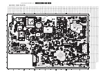
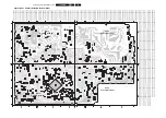
Circuit Diagrams and PWB Layouts
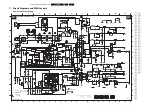
Diagram PWB
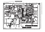
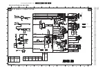
Mono Carrier: Power Supply
(A1) 4
15-20
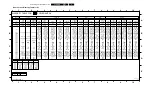
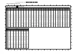
Mono Carrier: Diversity Table for A1
(A1) 5
15-20
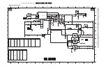
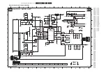
Mono Carrier: Deflection
(A2) 6
15-20
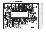
Mono Carrier: Diversity Table for A2
(A2) 7
15-20
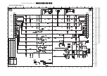
Mono Carrier: Tuner IF
(A3) 8
15-20
Mono Carrier: Hercules
(A4) 9
15-20
Mono Carrier: Features & Connectivities
(A5) 10
15-20
Mono Carrier: Class D - Audio Amplifier
(A6) 11
15-20
Mono Carrier: Audio Amplifier
(A7) 12
15-20
Mono Carrier: Rear I/O Scart
(A8) 13
15-20
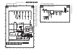
Mono Carrier: Front Control
(A9) 14
15-20
Mono Carrier: DVD Power Supply
(A10) 14
15-20
8.
Alignments
21
9.
Circuit Descriptions, List of Abbreviations, and IC
Data Sheets
21
10. Spare Parts List
22
11. Revision List
28


