
Published by LM 0367
Printed in the Netherlands
Subject to modification
EN 3122 785 12511
©
Copyright 2003 Philips Consumer Electronics B.V. Eindhoven, The Netherlands.
All rights reserved. No part of this publication may be reproduced, stored in a
retrieval system or transmitted, in any form or by any means, electronic,
mechanical, photocopying, or otherwise without the prior permission of Philips.
Colour Television
Chassis
LC1.15E
AA
Contents
Page
Safety Precautions
Servicing Precautions
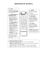
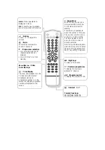
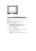
Description of Controls
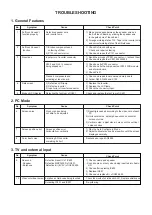
Troubleshooting
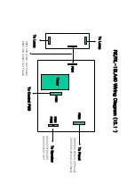
Wiring Diagram
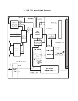
Block Diagram
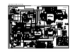
Main Board for LC151x01-A3 LCD Panel
Main Board PWB for LC151x01-A3 LCD Panel 12-13
Control and Tuner Panel PWB
Main Board for LC151x01-C3P1 LCD Panel
Main Board PWB for LC151x01-C3P1 LCD P.
Control and Tuner Panel PWB
Adjustment Instruction
Exploded View
Spare Parts List
Revision List
Summary of Contents for LC1.15E
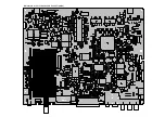
Page 12: ...Main Board for LC151X01 A3 LCD Panel Top Side ...
Page 13: ...Main Board for LC151X01 A3 LCD Panel Bottom Side ...
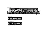
Page 14: ...CONTROL TUNER TOP TUNER BOTTOM ...
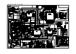
Page 15: ...Main Board for LC151X01 C3P1 LCD Panel ...
Page 16: ...Main Board for LC151X01 C3P1 LCD Panel Top Side ...
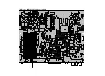
Page 17: ...Main Board for LC151X01 C3P1 LCD Panel Bottom Side ...
Page 18: ...CONTROL TUNER TOP TUNER BOTTOM ...
Page 21: ...EXPLODED VIEW 112 540 500 550 521 541 120 530 310 400 401 410 ...


