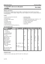
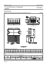
background image

DATA  SHEET

Product specification
File under Integrated Circuits, IC01

July 1994

INTEGRATED CIRCUITS

TDA1552Q
2 x 22 W BTL stereo car radio
power amplifier

Summary of Contents for TDA1552Q

Page 1: ...DATA SHEET Product specification File under Integrated Circuits IC01 July 1994 INTEGRATED CIRCUITS TDA1552Q 2 x 22 W BTL stereo car radio power amplifier ...

Page 2: ...ity safe Capability to handle high energy on outputs VP 0 V Protected against electrostatic discharge No switch on switch off plop Low thermal resistance Flexible leads QUICK REFERENCE DATA PACKAGE OUTLINE 13 lead SIL bent to DIL plastic power SOT141R SOT 141 6 1996 July 23 PARAMETER CONDITIONS SYMBOL MIN TYP MAX UNIT Supply voltage range operating VP 6 0 14 4 18 0 V non operating VP 30 V load dum...

Page 3: ...and by switch VP mute switch stand by reference voltage 3 10 VP1 VP2 18 kΩ 2 kΩ 18 kΩ 15 kΩ 15 kΩ 2 kΩ 18 kΩ 2 kΩ 18 kΩ 2 kΩ 60 kΩ 60 kΩ mute switch VA Cm power stage mute switch VA Cm power stage 4 6 11 12 mute switch VA Cm power stage mute switch VA Cm power stage 9 7 Vref 2 5 8 ground signal GND1 GND2 power ground substrate output 2B output 2A not connected output 1B input 1 input 2 13 1 TDA155...

Page 4: ...1 8 GND2 power ground 2 substrate 2 GND ground signal 9 OUT2B output 2B 3 VP1 positive supply voltage 1 10 VP2 positive supply voltage 2 4 OUT1A output 1A 11 M SS mute stand by switch 5 GND1 power ground 1 substrate 12 n c not connected 6 OUT1B output 1B 13 IP2 input 2 7 OUT2A output 2A PARAMETER CONDITIONS SYMBOL MIN MAX UNIT Supply voltage operating VP 18 V non operating VP 30 V load dump protec...

Page 5: ...July 1994 5 Philips Semiconductors Product specification 2 x 22 W BTL stereo car radio power amplifier TDA1552Q Fig 2 Power derating curve ...

Page 6: ...Total quiescent current Itot 80 160 mA DC output voltage note 2 VO 6 9 V DC output offset voltage VO 150 mV Mute stand by switch Switch on voltage level VON 8 5 V Mute condition Vmute 3 3 6 4 V Output signal in mute VI 1 V max position f 1 kHz VO 2 mV DC output offset voltage between pins 4 to 6 and 7 to 9 VO 150 mV Stand by condition Vsb 0 2 V DC current in VII 0 5 V Isb 100 µA stand by condition...

Page 7: ...ncy between 1 kHz and 10 kHz 8 Noise voltage measured in a bandwidth of 20 Hz to 20 kHz 9 Noise output voltage independent of RS VI 0 V PARAMETER CONDITIONS SYMBOL MIN TYP MAX UNIT Output power THD 0 5 Po 15 17 W THD 10 Po 20 22 W Output power at VP 13 2 V THD 0 5 Po 12 W THD 10 Po 17 W Total harmonic distortion Po 1 W THD 0 1 Power bandwidth THD 0 5 Po 1 dB w r t 15 W Bw 20 to Hz 15000 Low freque...

Page 8: ...A1552Q APPLICATION INFORMATION Fig 3 Application circuit diagram handbook full pagewidth MLB951 100 nF mute stand by switch 12 11 3 10 220 nF 1 4 6 220 nF 13 9 7 5 8 VP TDA1552Q 2200 µF 14 4 V not connected R 4 Ω L R 4 Ω L 60 kΩ 60 kΩ reference voltage 2 ground signal input 2 input 1 power ground substrate ...

Page 9: ... 48 0 38 24 0 23 6 20 0 19 6 10 3 4 v 0 8 12 2 11 8 1 7 e2 5 08 2 4 1 6 Eh 6 2 00 1 45 2 1 1 8 3 4 3 1 4 3 DIMENSIONS mm are the original dimensions Note 1 Plastic or metal protrusions of 0 25 mm maximum per side are not included 12 4 11 0 SOT141 6 0 5 10 mm scale Q j 0 25 w 0 03 x D L E A c A2 m L3 Q w M bp 1 d D Z e 2 e e x h 1 13 j Eh non concave view B mounting base side 92 11 17 95 03 11 DBS1...

Page 10: ...kage below the seating plane or not more than 2 mm above it If the temperature of the soldering iron bit is less than 300 C it may remain in contact for up to 10 seconds If the bit temperature is between 300 and 400 C contact may be up to 5 seconds DEFINITIONS LIFE SUPPORT APPLICATIONS These products are not designed for use in life support appliances devices or systems where malfunction of these ...

Reviews: