
Published by JH 0671 BG CD Customer Service
Printed in the Netherlands
Subject to modification
EN 3122 785 16510
©
Copyright 2006 Philips Consumer Electronics B.V. Eindhoven, The Netherlands.
All rights reserved. No part of this publication may be reproduced, stored in a
retrieval system or transmitted, in any form or by any means, electronic,
mechanical, photocopying, or otherwise without the prior permission of Philips.
Colour Television
Chassis
TES1.0E
LA
G_16510_000.ep
s
2
3
1106
Contents
Page
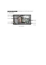
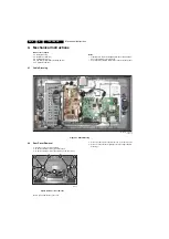
Technical Specifications, Connections, and Chassis
Overview
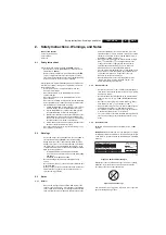
Safety Instructions, Warnings, and Notes
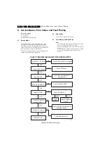
Service Modes, Error Codes, and Fault Finding 14
6.
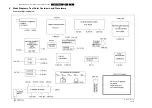
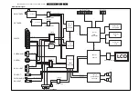
Block Diagrams, Test Point Overviews, and
Waveforms
Power Supply Block Diagram
15
Main Block Diagram
16
Switch Board Block Diagram
17
Main I2C Diagram
18
Tuner I2C Diagram
19
7.
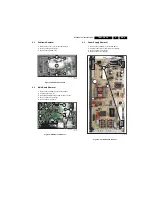
Circuit Diagrams and PWB Layouts
Diagram PWB
Main Board
20-29
30-31
Control Board
32
33
IR & LED Board
34
35
Mains Switch Board
36
37
Side I/O Board
38
39
Switch Board
40
41
8.
Alignments
43
9.
Circuit Descriptions, Abbreviation List, and IC Data
Sheets
45
Abbreviation List
46
IC Data Sheets
48
10. Spare Parts List
57
11. Revision List
75


