background image

Published by MB/SC 1363 Quality

Printed in the Netherlands

Subject to modification

EN 3122 785 19393

2013-Mar-29

2013 

©

 TP Vision Netherlands B.V.

All rights reserved. Specifications are subject to change without notice. Trademarks are the
property of Koninklijke Philips Electronics N.V. or their respective owners. 
TP Vision Netherlands B.V. reserves the right to change products at any time without being obliged to adjust
earlier supplies accordingly.
PHILIPS and the PHILIPS’ Shield Emblem are used under license from Koninklijke Philips Electronics N.V.

Colour Television

Chassis

VES1.1E

LA

See 

table of contents

 on page 3

Summary of Contents for VES1.1E

Page 1: ... notice Trademarks are the property of Koninklijke Philips Electronics N V or their respective owners TP Vision Netherlands B V reserves the right to change products at any time without being obliged to adjust earlier supplies accordingly PHILIPS and the PHILIPS Shield Emblem are used under license from Koninklijke Philips Electronics N V Colour Television Chassis VES1 1E LA See table of contents ...

Page 2: ...ferent set executions Specifications are indicative subject to change Technical Specifications For on line product support please use the links in Table 2 1 Here is product information available as well as getting started user manuals frequently asked questions and software drivers Table 2 1 Described model numbers Directions for Use You can download this information from the following websites ht...

Page 3: ...3113 U168 15 4 1 General Description 15 4 2 Absolute Ratings 16 4 2 1 Electrical Characteristics 16 4 2 2 Operating Specifications 17 4 3 Pinning 17 5 Power stage 18 5 1 Power management 21 6 Microcontroller MSTAR U5 23 6 1 Description 23 6 2 MSTAR block diagram 27 6 3 Reset circuit 28 7 CI interface 28 8 USB interface 29 9 DDR2 SDRAM K4T1G164QF U155 30 9 1 Description 30 9 2 Features 30 Pinning 3...

Page 4: ...eatures 38 14 3 Pin Assignment 40 15 LM1117 U175 U180 U181 41 15 1 General description 41 15 2 Features 41 15 3 Applications 41 15 4 Absolute maximum ratings 41 15 5 Pinning 42 16 MP2012 U176 42 17 General description 42 17 1 Features 42 17 2 Pinning 43 18 RTA8283A U23 U173 43 18 1 General description 43 18 2 Features 43 18 3 Pinning 45 19 MP1583 U174 46 19 1 General description 46 19 2 Features 4...

Page 5: ...s 57 23 10 1 Upload profile Data from USB 57 23 10 2 PQ Files Operations 57 23 10 3 Upload PQ files from USB 57 23 10 4 Ci credentials key update 57 23 10 5 HDCP keys update 57 23 10 6 Edid update 58 23 10 7 DDR settings update 58 23 10 8 MAC address update 58 23 11 Hotel Mode setup menu 58 23 11 1 Hotel TV welcome image update only available in Hotel TVs 58 24 Software update 59 25 Troubleshootin...

Page 6: ...ple transmission standards as B G D K I I and L L including German and NICAM stereo Also DVB T DVB C are supported internal demodulators of Mstar IC and DVB S S2 is supported with external demodulator Sound system output is supplying max 2 2 5 W less 10 THD at maximum output with 4 Ω speakers or 2 6 W for stereo 8 Ω speakers Supported peripherals are 1 RF input VHF I VHF III UHF 75 Ω Common 1 Side...

Page 7: ...1 1 General Block Diagram GPIO D3K Mstar VGA H DIJI1 i HPOErecr 2XIi H O UDI OAU Block Diagram V1 1 Drawn By Ulas Dere i 03 01 2011 ...

Page 8: ...ash U162 USB YPbPr SAV HP Satellite Tuner Keypad Speaker Con Tuner T3 External Keyboard Touchboard Main IC U5 HDMI Connectors VGA SCART Connec tor Led Con DVD Connector Power Connector LVDS Connectors DDR2 RAM U155 SPI Flash Adapter DC Input SPDIF Out Inv Con ...

Page 9: ...by circuits and microcontroller 2 1 General description of the Sony RE216 tuner The SUT RE216 is designed for terrestrial TV digital analog and digital cable reception It includes a full band tuner and a channel filtering for digital signals It provides a low IF output after channel filtering to drive a channel demodulator Tuning band switching and initialization are made via an I2 C bus interface...

Page 10: ... Programmable channel Filter bandwidth Fully I2 C bus controlled For Hybrid TV applications 3 3Vpullup 1000 1uF w AGC I 1KO o M h f N OIAocI ...

Page 11: ... 03 THD 85 efficiency 70 dB PSRR to improve RF rectification immunity AZAD2102B provide a Vibration Spectrum modulation clock for PWM Output This vibration frequency is around 10 kHz shift 5 kHz of Fpwm The advantage of the small size package WCSP makes AZAD2102B very suitable for mobile phone and PDA device application And the Class D amplifier structure let AZAD2102B to have highly efficiency po...

Page 12: ...t AVdd DVdd 3 6 Volt Rload 4Ω 0 30 Watts at AVdd DVdd 3 0 Volt Rload 4Ω 1 75 Watts at AVdd DVdd 5 5 Volt Rload 8Ω 0 87 Watts at AVdd DVdd 3 6 Volt Rload 8Ω 0 41 Watts at AVdd DVdd 3 0 Volt Rload 8Ω Eliminate Power on and Power off Pop noise A fewer external components Optimized PWM output stage eliminates LC output filter Internally generate 290 kHz switching frequency to eliminate capacitor and r...

Page 13: ...f 217Hz 68 dB Common mode rejection ratio Cf lRR VDD 3 0 V to 5 5 V Vic VDD 2 to 0 5 V Vi c VDD 2 to 0 5 VDD 0 8 V 65 dB H igh level nput current IIIHII VDD 5 5V Vi 5 8V 25 uA Low level Input current IIlLI VDD 5 5V Vi 0 3V 1 uA Operation current lop VDD 5 5 V no load 3 6 5 0 mA VDD 3 6 V no load 3 0 4 2 VDD 3 0 V no load 2 5 3 5 Output switching frequency Fpwm VDD 5 5 V no load 290 KHz VDD 3 6 V n...

Page 14: ...Total harmonic distortion plus noise VDD 5 0 V PO 1W RL 8 Q f 1kHz 0 15 VDD 3 6 V PO 0 5 W RL 8 Q f 1kHz 0 12 VDD 3 0 V PO 200 mW RL 8 Q f 1kHz 0 09 PSRR Supply ripple rejection ratio VDD 3 6 V Av 20V V Inputs connect to grounded with Ci l OJ JF F 217 H z VRipple 200 mVpp 67 dB SNR Signal to noise ratio VDD 5 V PO 1W RL 8 Q 95 dB Vnoise Output noise level VDD 3 6 V f 20 Hz to 20 kHz nputs ac groun...

Page 15: ... and a DC detection circuit The adjustable power limiter allows the user to set a virtual voltage rail lower than the chip supply to limit the amount of current through the speaker The DC detect circuit measures the frequency and amplitude of the PWM signal and shuts off the output stage if the input capacitors are damaged or shorts exist on the inputs The TPA3113D2 can drive stereo speakers as lo...

Page 16: ...Operation from 8 V to 26 V Filter Free Operation SpeakerGuard Speaker Protection Includes Adjustable Power Limiter plus DC Protection Flow Through Pin Out Facilitates Easy Board Layout Robust Pin to Pin Short Circuit Protection and Thermal Protection with Auto Recovery Option Excellent THD N Pop Free Performance Four Selectable Fixed Gain Settings Differential inputs 4 2 Absolute Ratings 4 2 1 Ele...

Page 17: ...C 7 p Analog supply AGNO 8 Analog signalground Connect to the thermal pad GVOO 9 0 High side FET gate drive supply Nominalvoltage is 7V Also should be used as supply for PLIMIT functi on PLIMIT 10 I Power limt i leveladjust Connect a resistor divider from GVOO to GND to set powerlimit Connect d irectly to GVOO for no power l imit R I NN 11 I Negative audio input for right channe l Biased at 3V R I...

Page 18: ...used for IPS60 IPS16 and IPS17 and CN1 is used for PW26 and PW27 JK9 is used for the adapter option and also CN705 inverter socket or DB32 chassis with CN706 is used to supply backlight The power supplies generate 18V 12V 5V 3 3V and 12V 5V stand by mode DC voltages Power stage which is on chassis generates 5V 3V3 stand by voltage and 12V 8V 5V 3V3 2 5V 1 8V and 1 2V supplies for other different p...

Page 19: ... block diagram is using dependent to main supply For PW26 and PW27 just common blocks are enough for proper operation For IPS16 IPS17 IPS60 below blocks must work properly For adapter case also below blocks are necessary ...

Page 20: ... for protecting chassis and main IC against damages when any Vcc supply shorts to ground Protect pin should be logic high while normal operation When there is a short circuit protect pin shold be logic low After any short detection SW forces LEDs on LED card to blink ...

Page 21: ...5 1 Power management Power Management with Adaptor Power Management with PW25 PW26 ...

Page 22: ... Power Management with IPS16 IPS17 IPS60 PW05 Power Management with PW03 PW04 PW07 ...

Page 23: ...rated including full SCART support with CVBS output The equipped MStar MACE 5 color engine is the latest masterpiece from MStar famous color engine series providing excellent video and picture quality in Full HD and large scale displaying system To meet the increasingly popular energy legislative requirements without the use of additional hardware the MSD9WB9PT 2 has an ultra low power standby mod...

Page 24: ...A2 EIA J demodulation o Supports NICAM FM AM demodulation o Supports MTS Mode Mono Stereo SAP in BTSC EIA J mode o Supports Mono Stereo Dual in A2 NICAM mode o Built in audio sampling rate conversion SRC o Audio processing for loudspeaker channel including volume balance mute tone EQ virtual stereo surround and treble bass controls o Advanced sound processing options available for example SRS1 BBE...

Page 25: ...essor o 3D motion video deinterlacer with motion object stabilizer o Edge oriented deinterlacer with edge and artifact smoother o Automatic 3 2 2 2 M N pull down detection and recovery o 3D multi purpose noise reduction for DTV or lousy air cable input o MPEG artifact removal including de blocking and mosquito noise reduction o Arbitrary frame rate conversion MStar Professional Picture Enhancement...

Page 26: ...ction 500KHz o Optimised for SFN channels with pre post cursive echoes inside outside the guard o Acquisition range 857kHz includes up to 3x 1 6 MHz transmitter offset o Meets Nordig Unified 1 0 3 D Book 5 0 EICTA E Book C Book test requirement o 400kHz internal carrier offset recovery range o 6 8 usecs echo cancellation at 7 Msym s o Supports IF low IF zero IF inputs o Ultra fast automatic blind ...

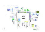
Page 27: ...6 2 MSTAR block diagram ...

Page 28: ...Reset condition is high and nomal working condition is low for RESET pin 7 CI interface CI Interface Power Switch It is used for CI module supply when Module is inserted it means CI detect is low This circuit is opened or closed by CI_POWER_CTRL port of main uController ...

Page 29: ...d for USB connectivity for last user Last user can play video picture and audio files Also digital channels can be record to external storage device by this interface All SW files can be updated with interface USB circuit has 3 main parts Integrated USB 2 0 Host interface of D3K U5 Protection IC U145 Over current protection IC U8 ...

Page 30: ...d to convey row column and bank address information in a RAS CAS multiplexing style For example 1Gb x8 device receive 14 10 3 addressing The 1Gb DDR2 device operates with a single 1 8V 0 1V power supply and 1 8V 0 1V VDDQ The 1 Gb DDR2 device is available in 60 ball FBGA x8 and 84ball FBGA x16 9 2 Features JEDEC standard VDD 1 8V 0 1V Power Supply VDDQ 1 8V 0 1V 533MHz fCK for 1066Mb sec pin 8 Ban...

Page 31: ... A3 AS A7 A9 Voo A12 NC VssQ UOQS VoDQ UOQS VssQ DQ15 VoDQ DQ8 VoDQ DQ10 VssQ OQ13 VssQ LDQS VoDQ LOQS VssQ OQ7 VoDQ DQO VoDQ OQ2 VssQ OQ5 VssoL CK Voo RAS CK OOT CAS cs A2 AO Voo A6 A4 A11 A8 Vss NC NC F G Pinning 1 2 3 7 8 9 Ball Locations x16 1 2 3 4 s 6 8 9 AB c D Populated ball Ball not popu lated Top view See theballs throughpackage E H KJ ML N p R ...

Page 32: ...y switch circuit This switch is used to open and close panel supply of TCON It is controlled by port of main ucontroller Also with this circit panel sequency could be adjusted correctly 3 panel supplys are connected to this circuit All of them are optional according to panels ...

Page 33: ...mand is executed on page 256 bytes basis and erase command is executes on chip or sector 4K bytes or block 64K bytes To provide user with ease of interface a status register is included to indicate the status of the chip The status read command can be issued to detect completion status of a program or erase operation via WIP bit When the device is not in operation and CS is high it is put in stand...

Page 34: ...t Operating Temperature 0 C to 70 C Storage Temperature 55 C to 125 C Applied Input Voltage 0 5v to 4 6v Applied Output Voltage 0 5v to 4 6v VCC to Ground Potential 0 5v to 4 6v 11 4 Pinning 8 PIN SOP 150mil SYMBOL DESCRIPTION CS Chip select SI Serial Data Input SO Serial Data Output SCLK Clock Input HOLD Hold to pause the device without deselecting the device VCC 3 3v Power Supply GND Ground ...

Page 35: ...densities without changing the footprint To extend the lifetime of NAND flash devices it is strongly recommended to implement an error correction code ECC The use of ECC correction allows to achieve up to 100 000 program erase cycles for each block A write protect pin is available to give a hardware protection against program and erase operations 12 2 Features High density NAND flash memories o 51...

Page 36: ...ique ID option Hardware data protection o Program erase locked during power transitions Data integrity o 100 000 program erase cycles with ECC o 10 years data retention RoHS compliant packages Development tools o Error correction code models o Bad blocks management and wear leveling algorithms 12 3 Pinning ...

Page 37: ...andard interfacing 13 2 Features Complete interface between LNB and I C bus Built in DC DC converter for single 12 V supply operation and high efficiency typ 93 0 5 A Selectable output current limit by external resistor Compliant with main satellite receivers output voltage specification Auxiliary modulation input EXTM pin facilitates DiSEqC 1 X encoding Accurate built in 22 kHz tone generator sui...

Page 38: ...sport stream The M88DS3002 supports symbol rate from 1 Msps up to 45 Msps and code rate from 1 4 to 9 10 Its features cover blind scan fade detection timing and carrier recovery performance monitoring co channel interference cancellation command interface and DiSEqC 2 X interface etc The device is controlled via a 2 wire serial bus The M88DS3002 works properly with 1 25 V and 3 3 V voltage supplie...

Page 39: ...ng loop acquisition Robust frame synchronization scheme Phase noise indicator Fast system recovery from fading or other abnormal conditions Co channel interference cancellation Constellation monitor Interface DVB S S2 common parallel and serial MPEG output interface compliant 2 wire serial bus to configure the device 2 wire bus repeater for tuner configuration DiSEqC 2 X compliant interface Genera...

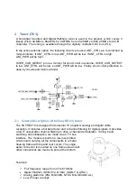
Page 40: ... Block Diagram of M88DS3002 14 3 Pin Assignment ...

Page 41: ... to as sure output voltage accuracy to within 1 The LM1117 series is available in SOT 223 TO 220 and TO 252 D PAK packages A minimum of 10μF tantalum capacitor is required at the output to improve the transient response and stability 15 2 Features Available in 1 8V 2 5V 2 85V 3 3V 5V and Adjustable Versions Space Saving SOT 223 Package Current Limiting and Thermal Protection Output Current 800mA L...

Page 42: ... cycle for low dropout applications With peak current mode control and internal compensation the MP2012 is stable with ceramic capacitors and small inductors Fault condition protection includes cycle by cycle current limiting and thermal shutdown 17 1 Features 2 7 6V Input Operation Range Output Adjustable from 0 8V to VIN 1 μA Max Shutdown Current Up to 95 Efficiency 100 Duty Cycle for Low Dropou...

Page 43: ...eliver up to 3A output current from a 4 5V to 23V input supply The RT8283A s current mode architecture and external compensation allow the transient response to be optimized over a wide range of loads and output capacitors Cycle by cycle current limit provides protection against shorted outputs and soft start eliminates input current surge during start up The RT8283A also provides output under vol...

Page 44: ......

Page 45: ...an internal res divider For an adjustable output an external res divider is connected to this pin 6 COMP Compensation Node COMP is used to compensate the regulation Control loop Connect a series RC network from COMP to GND In some cases an additional capacitor from COMP to GND is required 7 EN Enable Input Pin Logic high enables the converter a logic low forces the RT8253A into shutdown mode Attac...

Page 46: ...00mΩ Internal Power MOSFET Switch Stable with Low ESR Output Ceramic Capacitors Up to 95 Efficiency 20μA Shutdown Mode Fixed 385KHz Frequency Thermal Shutdown Cycle by Cycle Over Current Protection Wide 4 75V to 23V Operating Input Range Output Adjustable from 1 22V to 21V Under Voltage Lockout 19 3 Pinning Pin No Pin Name Description 1 BOOT High Side Gate Drive Bootstrap Input BS supplies the dri...

Page 47: ...ed using Fairchild s advanced PowerTrench process that has been especially tailored to minimize on state resistance and yet maintain low gate charge for superior switching performance These devices have been designed to offer exceptional power dissipation in a very small footprint for applications where the larger packages are impractical 20 2 Features Max rDS on 65 mΩ at VGS 4 5 V ID 4 0 A Max rD...

Page 48: ... s low voltage PowerTrench process It has been optimized for battery power management applications 21 2 Features 5 5 A 20 V RDS ON 33 mΩ VGS 4 5 V RDS ON 43 mΩ VGS 2 5 V RDS ON 60 mΩ VGS 1 8 V Fast switching speed High performance trench technology for extremely low RDS ON S 21 3 Pinning ...

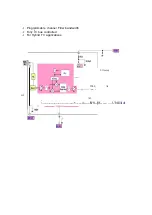
Page 49: ...22 Connectors 22 1 SCART SC1 22 2 HDMI CN707 CN708 ...

Page 50: ... 22 3 VGA CN711 15 14 VERTICALSYNC 15 DOC CLOCK _ ...

Page 51: ...played on the screen when the TV is in one of the TV AV PC modes It shows what the items are set in Profile Manager It is a read only screen not writable It shows the following items TV Life Time The number of minutes the set is in the On mode Standby SW Version The version number of the Stand by software Mboot Version The version number of the Mboot software PANEL The LCD panel identification inc...

Page 52: ...o Settings RF AGC adjustments for neighbour and image channels exist or don t Also ADC Calibration gain and offset values for RGB separately due to selected sources 23 3 Audio Settings Surround type and surround mode text items are displayed ...

Page 53: ...ons 1 Profile options such as AUTO TV off time Power up mode EPG type etc are displayed in options 1 23 5 Options 2 Profile options such as APS sorting Dynamic Menu Auto zoom mode etc are displayed in Options 2 ...

Page 54: ...ed Items which are connected to Tuner are picked off from menu Install and Retune Menu Channel List Menu 23 8 Diagnostic The result of various diagnostic tests are displayed here 23 9 USB operations USB operations are performed by pressing that button See Service Menu Design Idea for Menu structure look and feel position etc ...

Page 55: ...ion R Gain ADC Calibration G Gain ADC Calibration B Gain ADC Calibration R Offset ADC Calibration G Offset ADC Calibration B Offset Audio Settings Surround Type Surround Mode Text Options 1 Auto TV OFF Power Up mode Backlight Trick Mode Cable Support EPG Type Hotel Mode LCN PC Standby Stby Search Test Tool Local Key Volume Level Options 2 Aps Sorting Dynamic Menu EPG Menus Transparent Text ...

Page 56: ...EXT2 EXT2 S FAV S VIDEO HDMI 1 HDMI 2 HDMI 3 HDMI 4 YPBPR VGA PC Blu ray Diagnostic Remote control test UHF test VHF test Factory reset Tuner I2C IF I2C HDMI I2C Ethernet EDID Status HDCP Status DDR Settings CI Credentials MAC Address USB Operations Press this button to perform USB operations ...

Page 57: ...n service menu is pressed Whenever a USB stick is connected to TV set and USB Operations button in service menu is pressed pq folder is checked If it exists and if they include some files necessary copy delete operations are performed 23 10 3 Upload PQ files from USB 1 Create a folder named pq in the USB stick 2 Copy VESTEL_D1_Plus_PNL bin Titania2_Main bin and Titania2_Main_Text bin into USB pq f...

Page 58: ...en press the Home Menu button Note To order a yellow remote use order code 22AV8573 00 or 12NC 8670 000 67389 23 11 1 Hotel TV welcome image update only available in Hotel TVs In the VES1 1E LA the welcome image can be updated Copy To USB There are two steps and both are independent of each other Copy the updated welcome image to USB as hotel_wel png Copy NVRAM data service list preferences etc to...

Page 59: ...ned 4 If first time installation screen is displayed it means the software update procedure is successful 25 Troubleshooting 25 1 No backlight problem Problem If TV is working led is normal and there is no picture and backlight on the panel Possible couses Backlight pin dimming pin backlight supply stby on off pin Backlight pin should be high in open position If it is low please check Q181 and pan...

Page 60: ...Backlight power supply should be in panel specs Please check CN705 for the SSB related connectors for power supply cards ...

Page 61: ...77 25 2 CI module problem Problem CI is not working when CI module inserted Possible couses Supply suply control pin detect pins mechanical positions of pins CI supply shoul be 5V when CI module inserted If it is not 5V please check CI_POWER_CTRL this pin should be low ...

Page 62: ... low If it is not low please check the Cl connector pins Cl module pins and 3V3_VCC on the SSB R1632 PCM D3 PCM D4 4 PCM DS Cl Detect PCM D6 7 PCM CB N 8 PCM AlO PCM OB_N 10 PCM All 11 PCM A9 12 PCM AS 13 PCM A13 14 PCM A14 3V3_VCC 21 22 23 12p 24 sov 25 27 28 29 Cl Detect 30 A 31 ...

Page 63: ...n should be logic high while normal operation When there is a short circuit protect pin will be logic low If you detect logic low on protect pin unplug the TV set and control voltage points with a multimeter to find the shorted voltage to ground 25 4 IR problem Problem LED or IR not working Check LED card supply on the SSB ...

Page 64: ...LED SOCKET Ql70 L J SV STBY F259 2 IR IN C949 600R H N Ql7l 25 5 Keypad touchpad problems Problem Keypad or Touchpad is not working BC949B Check keypad supply and keyboard pin on the SSB ...

Page 65: ...25 6 USB problems Problem USB is not working or no USB Detection Check USB Supply It should be nearly 5V 25 7 No sound problem Problem No audio at main TV speaker outputs ...

Page 66: ...t when headphone is connected speakers are automatically muted Measure voltage at HP_DETECT pin it should be 3 3v 25 8 No sound problem at headphone Problem No audio at headphone output Check HP detect pin when headphone is Check 5V_VCC and 3V3_VCC with a voltage meter 25 9 Standby On Off problem Problem Device cannot boot TV hangs in standby mode ...

Page 67: ...touts via hyper terminal or Teraterm These printouts may give a clue about the problem 25 10 DVD problems Problem DVD is not working Check that DVD source is selected in Service menu Check supply voltage of DVD namely 12V_VCC 25 11 No signal problem Problem No signal in TV mode Check tuner supply voltage 3V3_TUN Check tuner options are correctly set in Service menu Check AGC voltage at IF_AGC pin ...

Page 68: ......

Page 69: ...ng sheet 1 1 DISPLAYASM32 LED 8 METAL FRAME 32 LED SCREW P C ZN YFMB 3 x 9 5 1 IR 17LD98 1 1 1 3 5 6 7 11 9 10 2 1 COVER FOOT 2 ASM BACK COVER 32130 LED DVD 1 4 8 BACK COVER METAL 32130 SCREW P C ZN Y 10 11 1 2 ...

Page 70: ... 1 2 50V C62 2p2 C63 2p2 50V 33p C35 50V 50V 1n C19 10k R4 L1 4n7 IF_AGC_TUNER 47R R1583 1 2 3 4 5 6 7 8 R4 R1 R3 R2 TS_MDI3 TS_MDI2 TS_MDI1 TS_MDI4 TS_MDI5 TS_MDI6 TS_MDI7 3V3_S2_VDDA 10p C8 10p C9 S2_IN C30 16V 10n 10n C31 16V C32 10n 16V S2_QN 10p C10 C11 10p S2_QP 3V3_S2_VDDD 10V C38 100n 1V25_S2_VDDI 1V25_S2_VDDI 3V3_S2_VDDA 10V C36 100n 100n C37 10V SDA_S2_TUN SCL_S2_TUN R13 4k7 1 2 4k7 R14 ...

Page 71: ...C378 16V C120 100n C5V6 D171 3n3 C856 50V F202 600R 1 2 CDA4C16GTH D2 1 2 3 4 5 6 7 8 4n7 50V C858 SC_AUD_R_OUT D1 CDA4C16GTH 1 2 3 4 5 6 7 8 C853 50V 3n3 C835 50V 220p 1 2 C833 50V 220p 1 2 3n3 C854 50V SC_AUD_R_IN 600R F206 1 2 C831 220p 50V 1 2 100R R1245 1 2 F201 600R 1 2 SCART_AUD_R_IN SCART_AUD_L_IN RX SCL_SC TX SDA_SC C836 220p 50V 1 2 75R R1482 1 2 SC_CVBS_OUT C832 50V 220p 1 2 R1182 4k7 1...

Page 72: ...1 2 R1953 4k7 3V3_VCC CI_POWER_CTRL 50V C969 12p C687 10V 220n R1496 4k7 3V3_VCC R1660 4k7 1 2 33R R1942 6V3 22u C970 BACKLIGHT_ON OFF R344 1k2 33k R1605 R1604 33k R1607 18k 18k R1606 HDMI1_5V HDMI0_5V BC848B Q181 1 2 3 R1661 4k7 1 2 R1662 1k2 3V3_VCC S81 U162 NAND512 A 1 2 3 4 5 6 7 8 9 10 11 12 13 14 15 16 17 18 19 20 21 22 23 24 25 26 27 28 29 30 31 32 33 34 35 36 37 38 39 40 41 42 43 44 45 46 ...

Page 73: ...900 100R C1184 50V 4n7 220k R1898 DSP_MAIN_R DSP_MAIN_L MAIN_L MAIN_R R1904 10k R1919 12k 470p C1190 50V 10k R1903 R1918 12k SC_AUD_L_IN 10k R1901 12k R1920 470p C1188 50V SAV_L_IN C1189 50V 470p SC_AUD_R_IN 470p 50V C1187 SAV_R_IN R1921 12k 10k R1902 SCART_AUDIO_IN_R SCART_AUDIO_IN_L SAV_AUDIO_IN_L SAV_AUDIO_IN_R 22k R1925 1 2 R1924 22k 1 2 SC_R_OUT SC_L_OUT 50V 100p C1186 DSP_SCART_L DSP_SCART_R...

Page 74: ... 10u C1032 16V HP_R D203 C5V6 Q210 2N7002 1u 25V C1074 6V3 C1078 1u AMP_EN C1172 16V 10n F296 60R R623 4k7 VDD_AUDIO R1855 10k 1 2 R817 100R BC848B Q133 1 2 3 100R R818 VDD_AUDIO 10V 220n C602 L_AUDIO_P_OUT L_AUDIO_N_OUT MAIN_L 4k7 R624 C665 100n 10V 1 2 10V 220n C608 AMP_EN VDD_AUDIO 3V3_VCC 10k R1309 10k R616 3V3_STBY L_AUDIO_N L_AUDIO_P R_AUDIO_N PT2333 U164 C3 C2 C1 B3 B2 B1 A3 A2 A1 INP GNDA ...

Page 75: ... 33k OP_PIN27 BACKLIGHT_ON OFF PANEL_VCC R54 10k 1 2 33k R66 CI_POWER_CTRL R1671 4k7 1 2 4k7 R1672 1 2 R1952 4k7 1 2 LED1 LED2 3V3_STBY 3V3_STBY OP_PIN11 PANEL_VCC 10k R55 1 2 R67 33k MEGA_DCR_IN OP_PIN8 S2 MEGA_DCR_OUT PANEL_VCC 33k R72 R56 10k 1 2 OP_PIN9 OP_PIN10 PANEL_VCC 10k R57 1 2 33k R68 33k R69 OP_PIN7 PANEL_VCC 10k R58 1 2 R70 33k OP_PIN6 PANEL_VCC R59 10k 1 2 33k R71 OP_PIN5 PANEL_VCC 1...

Page 76: ... 3 4 5 6 7 8 A B C D E F A3 PROJECT NAME SCH NAME DRAWN BY T SHT VDDC_1V2 C68 50V 15n 15k R43 C12 220n 25V D7 1N4001 LNB_OUT C70 470n 25V 3V3_VCC R19 10k F295 1k SK24 D8 C13 220n 25V 16V C997 100n SDA_SYS SCL_SYS 3V3_VCC 100n 16V C1005 C14 25V 220n C1070 16V 100n C1004 16V 100n LNBH23L U6 27 4 19 18 6 9 14 29 30 22 13 21 11 12 1 2 3 7 8 16 17 23 24 25 26 31 32 10 15 28 5 20 A_GND P_GND I_SEL BYP A...

Page 77: ...S 39k R1686 1V2_VCC 10n C1113 16V 1 2 5n6 C1131 50V 1 2 60R F273 1 2 R1710 3k9 1 2 R1720 100R 1 2 33k R1731 1 2 C1048 220n 25V 1 2 47R R1723 1 2 12V_STBY Q183 BC848B 1 2 3 3V3_STBY 22k R1735 R1730 10k 5V_STBY MOSFET_CONTROL 3V3_VCC L118 15u 1 2 1k R1768 C1084 16V 22u R1737 33k C1035 100n 10V 1 2 C1080 6V3 100u 1 2 R1709 3k9 1 2 5n6 50V C1130 1 2 16V 10n C1112 1 2 D197 SS33 1 2 MP1583 U174 5 6 7 8 ...

Page 78: ...27 2 PSU ...

Page 79: ......

Reviews: