background image

USER 
MANUAL 

SP-7165/7167 

15” / 17” Fanless Panel PC 

Powered by Intel

® 

Core

TM

i7/i5/i3 / Pentium

® 

/ Celeron

®


CPU Processor 


SP-7165/7167 M1 

Summary of Contents for SP-7165

Page 1: ...USER MANUAL SP 7165 7167 15 17 Fanless Panel PC Powered by Intel CoreTM i7 i5 i3 Pentium Celeron CPU Processor SP 7165 7167 M1 ...

Page 2: ...ransmit in any form or by any means electronic or mechanical including photocopying and recording DISCLAIMER This user s manual is meant to assist users in installing and setting up the system The information contained in this document is subject to change without any notice CE NOTICE This is a class A product In a domestic environment this product may cause radio interference in which case the us...

Page 3: ...ons to the equipment not expressly approved by the party responsible for compliance could void your authority to operate such equipment CAUTION Danger of explosion may occur when the battery is incorrectly replaced Replace the battery only with the same or equivalent type recommended by the manufacturer Dispose of used batteries according to the manufacturer s instructions WARNING Some internal pa...

Page 4: ... Connector Quick Reference Table 3 15 3 4 Component Locations Of System Main Board 3 17 3 4 1 Top View and Jumper Settings of SB 8400 3 17 3 4 2 Bottom View of SB 8400 3 19 3 5 How To Set Jumpers 3 20 3 6 Function Buttons and I O Ports 3 22 3 6 1 Power Button 3 22 3 6 2 DC IN Port For SP 7165 SP 7167Rx x0x 3 22 3 6 3 DC IN 3 Pins Terminal Block For SP 7165 SP 7167Rx x1x 3 23 3 7 Setting Connectors...

Page 5: ...38 3 7 15 LVDS Connector 3 39 3 7 16 LVDS Inverter Connector 3 39 3 7 17 PCI Express Slot x4 3 40 3 7 18 Control Signal Connector 3 41 3 7 19 I2C Wafer optional 3 42 3 7 20 Power Button Connectors 3 42 3 7 21 Panel Power LED Connector 3 43 3 7 22 Panel HDD LED Connector 3 43 3 7 23 Low Pin Count LPC Connector 3 44 3 7 24 CompactFlash Card Connector 3 45 3 7 25 SIM Card Slot 3 46 3 7 26 Hardware Po...

Page 6: ... 3 LVDS Panel Signal Connector Connected To LCD Panel 3 57 3 10 4 15 Panel LED Backlight Control Connector 3 58 3 10 5 Touch Panel Connector 3 58 3 10 6 LED1 Connector 3 59 3 10 7 Touch Panel Up Signal Setting 3 60 3 10 8 Touch Panel Low Signal Setting 3 61 4 Software Utilities 4 1 4 1 Introduction 4 2 4 2 Installing Intel Chipset Software Installation Utility 4 4 4 2 1 Introduction 4 4 4 2 2 Inte...

Page 7: ...y 5 3 5 3 Main 5 6 5 4 Advanced 5 8 5 4 1 Advanced CPU Configuration 5 9 5 4 2 Advanced PCH FW Configuration 5 11 5 4 3 Advanced Trusted Computing 5 12 5 4 4 Advanced ACPI Settings 5 13 5 4 6 Advanced SATA Configuration 5 14 5 4 7 Advanced Hardware Monitor 5 15 5 4 8 Advanced F81866 Watchdog Configuration 5 16 5 4 9 Advanced F81866 Super IO Configuration 5 17 5 4 10 Advanced Network Stack Configur...

Page 8: ...65 LCD Display Exploded Diagram Projected Touch Screen A 6 SP 7167 LCD Display Exploded Diagram 5 Wire Resistive Touch Screen A 8 SP 7167 LCD Display Exploded Diagram Projected Touch Screen A 10 SP 7165 SP 7167 Module PC Exploded Diagram A 12 SP 7165 SP 7167 1st Memory Slot CPU Installation Exploded Diagram A 14 SP 7165 SP 7167 2nd Memory Slot and SSD Installation Exploded Diagram A 15 SP 7165 Pan...

Page 9: ...vi Configuring WatchDog Timer B 25 Flash BIOS Update B 27 ...

Page 10: ...vii Revision History The revision history of SP 7165 SP 7167 User Manual is described below Version No Revision History Page No Date M1 Initial Release 2018 01 ...

Page 11: ... 7167 SERIES USER MANUAL Page 1 1 1 Introduction This chapter provides the introduction for the SP 7165 SP 7167 system as well as the framework of the user manual The following topic is included About This Manual ...

Page 12: ...em Read the safety reminders carefully on how to take care of your system properly Chapter 3 System Configuration This chapter describes the locations and functions of the system motherboard components You will learn how to properly configure the connectors and system configuration jumpers on the motherboard and configure the system to meet your own needs Chapter 4 Software Utilities This chapter ...

Page 13: ... the SP 7165 SP 7167 system It describes how to set up the system quickly and outlines the system specifications The following topics are included Package List System Overview System Specification Safety Precautions Experienced users can go to Chapter 3 System Configuration on page 3 1 for a quick start ...

Page 14: ...65 SP 7167 SERIES USER MANUAL Page 2 2 2 1 Package List If you discover any of the items listed below are damaged or lost please contact your local distributor immediately Item Q ty SP 7165 SP 7167 1 Manual Driver DVD 1 Quick Guide 1 ...

Page 15: ...Chapter 2 Getting Started SP 7165 SP 7167 SERIES USER MANUAL Page 2 3 2 2 System Overview Unit mm SP 7165 Front View Rear View Top View ...

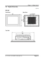
Page 16: ...Chapter 2 Getting Started SP 7165 SP 7167 SERIES USER MANUAL Page 2 4 Side View ...

Page 17: ...Chapter 2 Getting Started SP 7165 SP 7167 SERIES USER MANUAL Page 2 5 Bottom View Quarter View ...

Page 18: ...Chapter 2 Getting Started SP 7165 SP 7167 SERIES USER MANUAL Page 2 6 Unit mm SP 7167 Front View Rear View Top View ...

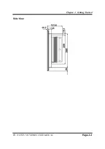
Page 19: ...Chapter 2 Getting Started SP 7165 SP 7167 SERIES USER MANUAL Page 2 7 Side View ...

Page 20: ...Chapter 2 Getting Started SP 7165 SP 7167 SERIES USER MANUAL Page 2 8 Bottom View Quarter View ...

Page 21: ...70 SKU only Audio 1 x Line in 1 x Line out 1 x Mic in Expansion Slot 1 x Full sized mini PCIe mini PCIe USB and SIM signals 1 x Half sized mini PCIe mini PCIe and USB signals 1 x SIM card slot 1 x CFast slot System Weight SP 7165 8 9 kg SP 7167 10 9 kg Operating System Windows 7 64 bit Windows 8 1 64 bit Windows 10 loT LTSB 2016 64 bit Linux Ubuntu 16 04 Dimension W x H x D SP 7165 408 x 320 x 121...

Page 22: ...ptional Audio 1 x Line in 1 x Line out 1 x Mic in Power Input DC in 9 36V DIN type 4 pin connector or 3 pin terminal block LED 1 x Power LED 1 x HDD LED 2 x PoE active LED optional Power On Off 1 x power button 1 x remote switch Display LCD SP 7165 15 TFT LCD LED Resolution XGA 1024 x768 SP 7167 17 TFT LCD LED Resolution SXGA 1280 x 1024 Touch Screen 5 wire resistive touch screen or projected USB ...

Page 23: ...m rapidly from a hot place to a cold place and vice versa because condensation may occur inside the system Protect your SP 7165 SP 7167 from strong vibrations which may cause hard disk failure Do not place the system too close to any radio active device Radio active device may cause signal interference Always shut down the operating system before turning off the power 3 Handling Avoid placing heav...

Page 24: ...and component locations for the main board The following topics are included SP 7165 SP 7167 Bottom I O Ports Diagrams Connector Jumper Quick Reference Table System Main Board Component Locations How to Set Jumpers Setting Main Board Connectors and Jumpers Touch Control Board Component Locations Setting Touch Control Board Connectors and Jumpers ...

Page 25: ...hapter 3 System Configuration SP 7165 SP 7167 SERIES USER MANUAL Page 3 14 3 1 External I O Ports Diagram 3 2 SP 7165 SP 7167 Bottom I O Ports Diagram For SP 7165 SP 7167Rx x0x For SP 7165 SP 7167Rx x1x ...

Page 26: ... Selection JP17 CONNECTOR Description NAME Mainboard Front Side Connectors COM Port COM1 COM2 COM3 COM4 LAN1 LAN2 Ports LAN1 LAN2 4 x 1 USB 3 0 Connectors USB1 Optional Digital Input Output Connector DIO1 DVI I Connector DVI1 HD Audio Connector AUDIO1 Full Sized Mini PCI Express Slot M_PCIE1 Half Sized Mini PCI Express Slot M_PCIE2 SATA 3 0 Connectors SATA1 SATA2 SATA Power Connectors SATA_PWR1 SA...

Page 27: ... 16 CONNECTOR Description NAME Panel Power LED Connector PWRLED1 Panel HDD LED Connector HDDLED1 Low Pin Count LPC Connector JLPC1 CFast Card Slot CFAST1 DDR4 SO DIMM memory socket SO DIMM1 Mainboard Rear Side Connector SIM Card Slot SIM1 DDR4 SO DIMM memory socket SO DIMM2 ...

Page 28: ... 3 System Configuration SP 7165 SP 7167 SERIES USER MANUAL Page 3 17 3 4 Component Locations Of System Main Board 3 4 1 Top View and Jumper Settings of SB 8400 Figure 3 1 Main Board Component Location Top View ...

Page 29: ... properly grounded CAUTION Observe precautions while handling electrostatic sensitive components Make sure to ground yourself to prevent static charge while you are working on the connectors and jumpers Use a grounding wrist strap and place all electronic components in any static shielded devices CAUTION Always touch the motherboard components by the edges Never touch components such as a processo...

Page 30: ...Chapter 3 System Configuration SP 7165 SP 7167 SERIES USER MANUAL Page 3 19 3 4 2 Bottom View of SB 8400 Figure 3 2 Main Board Component Location Rear View ...

Page 31: ...tings by opening or closing jumpers Jumpers can be combined into sets that are called jumper blocks When jumpers are all in the block you have to put them together to set up the hardware configuration The figure below shows what this looks like Jumpers Caps If a jumper has three pins for example labeled 1 2 and 3 You can connect pins 1 and 2 to create one setting and shorting You can also select t...

Page 32: ...Chapter 3 System Configuration SP 7165 SP 7167 SERIES USER MANUAL Page 3 21 Jumper diagrams Jumper settings ...

Page 33: ... the Power button located on the left side of Bottom I O panel ACTION ASSIGNMENT Press 0V Release PWRBTN 3 6 2 DC IN Port For SP 7165 SP 7167Rx x0x Port Name DC IN Description DC Power In Port PIN ASSIGNMENT PIN ASSIGNMENT 1 GND 2 GND 3 12V 4 12V Note The 4 pin DC IN port DIN is not supported in SP 7165 SP 7167Rx x1x Power Button DC IN ...

Page 34: ...ER MANUAL Page 3 23 3 6 3 DC IN 3 Pins Terminal Block For SP 7165 SP 7167Rx x1x Port Name DC IN Description DC IN 3 pins terminal block PIN ASSIGNMENT 1 VCC 9 36 VDC 2 3 GND Note The 3 pin DC IN terminal block is not supported in SP 7165 SP 7167Rx x0x DC IN ...

Page 35: ...ment PIN ASSIGNMENT RS232 Default Setting RS422 RS485 10 DCD TX RS 485 11 RX TX RS 485 12 TX RX X 13 DTR RX X 14 GND GND GND 15 DSR X X 16 RTS X X 17 CTS X X 18 RI X X Notes 1 COM1 Pin 9 and COM2 pin 18 are selectable for RI 5V or 12V by jumper setting Default setting is RI please see COM1 Pin9 and COM2 PIN18 Definition Selection Guide for selection details 2 COM1 COM2 is selectable as RS232 RS422...

Page 36: ...AL Page 3 25 COM3 RS232 Connector Pin Assignment PIN ASSIGNMENT PIN ASSIGNMENT 1 DCD 6 DSR 2 RX 7 RTS 3 TX 8 CTS 4 DTR 9 RI 5 GND COM4 RS232 Connector Pin Assignment PIN ASSIGNMENT PIN ASSIGNMENT 10 DCD 15 DSR 11 RX 16 RTS 12 TX 17 CTS 13 DTR 18 RI 14 GND COM3 COM4 ...

Page 37: ...nd COM2 PIN18 Definition Selection Guide Jumper Location JP12 JP15 Description COM1 pin9 JP12 and COM2 pin18 JP15 RI 5V 12V Selection SELECTION JUMPER SETTING JUMPER ILLUSTRATION RI 1 2 Default Setting JP12 JP15 12V 3 4 JP12 JP15 5V 5 6 JP12 JP15 2 1 6 5 2 1 6 5 2 1 6 5 2 1 6 5 2 1 6 5 2 1 6 5 ...

Page 38: ...ption LAN1 LAN2 Port LAN RJ 45 Port Bottom I O LAN1 Intel PHY I219 LM 10 100 1000Mbps LAN2 Intel LAN I210 AT 10 100 1000Mbps PIN ASSIGNMENT A1 MDI_1D0 A2 MDI_1D0 A3 MDI_1D1 A4 MDI_1D1 A5 MDI_1D2 A6 MDI_1D2 A7 MDI_1D3 A8 MDI_1D3 B1 MDI_2D0 B2 MDI_2D0 B3 MDI_2D1 B4 MDI_2D1 B5 MDI_2D2 B6 MDI_2D2 B7 MDI_2D3 B8 MDI_2D3 LAN1 LAN2 ...

Page 39: ...ttom side of the system By observing their status you can know the status of the Ethernet connection LAN LED Indicator Left Side LED Green Color On 10 100Mbps LAN Speed Indicator Yellow Color On Giga LAN Speed Indicator Off No LAN Switch HUB connected Right Side LED Yellow Color Blinking LAN Message Active Off No LAN Message Active ...

Page 40: ...MENT PIN ASSIGNMENT A1 5V A9 USB3_TX1 A2 USB_D1 A8 USB3_TX1 A3 USB_D1 A7 GND A4 GND A6 USB3_RX1 A5 USB3_RX1 B1 VCC5 B9 USB3_TX2 B2 USB_D2 B8 USB3_TX2 B3 USB_D2 B7 GND B4 GND B6 USB3_RX2 B5 USB3_RX2 C1 5V C9 USB3_TX3 C2 USB_D3 C8 USB3_TX3 C3 USB_D3 C7 GND C4 GND C6 USB3_RX3 C5 USB3_RX3 D1 VCC5 D9 USB3_TX4 D2 USB_D4 D8 USB3_TX4 D3 USB_D4 D7 GND D4 GND D6 USB3_RX4 D5 USB3_RX4 USB1 ...

Page 41: ...DIN1 2 DOUT1 3 DIN2 4 DOUT2 5 DIN3 6 DOUT3 7 DIN4 8 DOUT4 9 DIN5 10 DOUT5 11 DIN6 12 DOUT6 13 DIN7 14 DOUT7 15 DIN8 16 DOUT8 System Digital I O Port DSUB 25 pins bottom I O PIN ASSIGNMENT PIN ASSIGNMENT 1 DIN1 14 DOUT1 2 DIN2 15 DOUT2 3 DIN3 16 DOUT3 4 DIN4 17 DOUT4 5 DIN5 18 DOUT5 6 DIN6 19 DOUT6 7 DIN7 20 DOUT7 8 DIN8 21 DOUT8 9 22 10 23 11 24 12 25 13 Note The 25 pin D Sub DIO connector is not ...

Page 42: ...GNMENT PIN ASSIGNMENT 1 DIN1 2 DOUT1 3 DIN2 4 DOUT2 5 DIN3 6 DOUT3 7 DIN4 8 DOUT4 9 DIN5 10 DOUT5 11 DIN6 12 DOUT6 13 DIN7 14 DOUT7 15 DIN8 16 DOUT8 System 16 pins terminal block DIO Port PIN ASSIGNMENT 1 DIN1 2 DIN2 3 DIN3 4 DIN4 5 DIN5 6 DIN6 7 DIN7 8 DIN8 9 DOUT1 10 DOUT2 11 DOUT3 12 DOUT4 13 DOUT5 14 DOUT6 15 DOUT7 16 DOUT8 Note The 16 pin terminal block DIO port is not supported in SP 7165 SP...

Page 43: ... DVI Digital Visual Interface Integrated Connector PIN ASSIGNMENT PIN ASSIGNMENT 1 TMDS_D2 13 NC 2 TMDS_D2 14 5V 3 GND 15 GND 4 NC 16 TMDS_HPD 5 NC 17 TMDS_D0 6 TMDS_CLK 18 TMDS_D0 7 TMDS_DATA 19 GND 8 VSYNC 20 NC 9 TMDS_D1 21 NC 10 TMDS_D1 22 GND 11 GND 23 TMDS_D3 12 NC 24 TMDS_D3 C1 RED C2 GREEN C3 BLUE C4 HSYNC C5 GND C6 DVI1 ...

Page 44: ...33 3 7 8 HD Audio Connector Connector Location AUDIO1 Description HD Audio Connector for Line_in Line_out Mic_in PIN ASSIGNMENT 2 MIC_IN_L 3 GND 1 GND 4 GND 5 MIC_IN_R 22 LINE_OUT_L 23 GND 24 GND 25 LINE_OUT_R 32 LINE_IN_L 33 GND 34 GND 35 LINE_IN_R 42 NC 43 NC 44 NC AUDIO1 ...

Page 45: ...NMENT 1 WAKE 2 3 3V_SB 3 NC 4 GND 5 NC 6 1 5V 7 CLKREQ 8 SIM_PWR 9 GND 10 SIM_DAT 11 REFCLK 12 SIM_CLK 13 REFCLK 14 SIM_RST 15 GND 16 SIM_VPP 17 SIM_SW1 18 GND 19 SIM_SW2 20 NC 21 GND 22 PERST 23 PE_RX7 24 3 3V_SB 25 PE_RX7 26 GND 27 GND 28 1 5V 29 GND 30 SMB_CLK 31 PE_TX7 32 SMB_DATA 33 PE_TX7 34 GND 35 GND 36 USB_D9 37 GND 38 USB_D9 39 3 3V_SB 40 GND 41 3 3V_SB 42 NC 43 GND 44 NC 45 NC 46 NC 47 ...

Page 46: ...D 22 PERST 23 PE_RX8 24 3 3V_SB 25 PE_RX8 26 GND 27 GND 28 1 5V 29 GND 30 SMB_CLK 31 PE_TX8 32 SMB_DATA 33 PE_TX8 34 GND 35 GND 36 USB_D10 37 GND 38 USB_D10 39 3 3V_SB 40 GND 41 3 3V_SB 42 NC 43 GND 44 NC 45 NC 46 NC 47 NC 48 1 5V 49 NC 50 GND 51 NC 52 3 3V_SB Mini PCI Express is the successor of the Mini PCI card and provides an increased data throughput The cards have a detached network interfac...

Page 47: ...Connector Location SATA1 and SATA2 Description Serial ATA 3 0 Connectors Serial ATA 3 0 Connector 1 SATA1 signals PIN ASSIGNMENT 1 GND 2 SATA_TX 3 SATA_TX 4 GND 5 SATA_RX 6 SATA_RX 7 GND Serial ATA 3 0 Connector 2 SATA2 signals PIN ASSIGNMENT 1 GND 2 SATA_TX1 3 SATA_TX1 4 GND 5 SATA_RX1 6 SATA_RX1 7 GND SATA1 SATA2 ...

Page 48: ...3 7 12 SATA Power Connectors Connector Location SATA_PWR1 and SATA_PWR2 Description Serial ATA Power Connectors Serial ATA Power Connector 1 SATA_PWR1 signals PIN ASSIGNMENT 1 5V 2 GND Serial ATA Power Connector 2 SATA_PWR2 signals PIN ASSIGNMENT 1 5V 2 GND SATA_PWR1 SATA_PWR2 ...

Page 49: ...t Connector Connector Location PWR_IN1 Description Power Input Connector PIN ASSIGNMENT PIN ASSIGNMENT 1 GND 2 GND 3 12V 4 12V 3 7 14 DC Power Input Connector Connector Location ATX_PWR1 Description DC Power Input Connector PIN ASSIGNMENT PIN ASSIGNMENT 3 12V 4 12V 1 GND 2 GND ATX_PWR1 PWR_IN1 ...

Page 50: ..._D2 5 GND 8 GND 7 LVDS1_D2 10 LVDS1_D1 9 LDVS1_D1 12 LVDS1_D3 11 LVDS1_D3 14 LVDS1_D0 13 LVDS1_D0 16 LVDS0_CLK 15 GND 18 GND 17 LVDS0_CLK 20 LVDS0_D2 19 LVDS0_D2 22 LVDS0_D1 21 GND 24 GND 23 LVDS0_D1 26 LVDS0_D0 25 LVDS0_D0 28 LVDS0_D3 27 LVDS0_D3 30 LVDS_VCC 29 LVDS_VCC 3 7 16 LVDS Inverter Connector Connector Location INV1 Description LVDS Inverter Connector PIN ASSIGNMENT 1 12V 2 12V 3 GND 4 BR...

Page 51: ...D B5 SMB_CLK A5 NC B6 SMB_DATA A6 NC B7 GND A7 NC B8 3 3V A8 NC B9 NC A9 3 3V B10 3 3V_AXU A10 3 3V B11 WAKE A11 PERST B12 RSVD A12 GND B13 GND A13 REFCLK B14 HSOP0 A14 REFCLK B15 HSON0 A15 GND B16 GND A16 HSIP0 B17 PRSNT 2 A17 HSIN0 B18 GND A18 GND B19 HSOP1 A19 RSVD B20 HSON1 A20 GND B21 GND A21 HSIP1 B22 GND A22 HSIN1 B23 HSOP2 A23 GND B24 HSON2 A24 GND B25 GND A25 HSIP2 B26 GND A26 HSIN2 B27 H...

Page 52: ...ignal Connector Connector Location SGN_BRD1 Description Control Signal Connector PIN ASSIGNMENT PIN ASSIGNMENT 1 VCC5A 2 VCC5A 3 USB_N 4 VCC12 5 USB_P 6 VCC12 7 GND 8 VCC12 9 LVDS_BKLTEN 10 VCC12 11 USB_N 12 VCC12 13 USB_P 14 HDD_LED 15 GND 16 PWR_LED 17 GND 18 BRCTR 19 VCC5 20 USB_OC SGN_BRD1 ...

Page 53: ...fer PIN ASSIGNMENT PIN ASSIGNMENT 1 I2C_SDA 2 I2C_SCL 3 I2C_SDA 4 I2C_SCL 3 7 20 Power Button Connectors Connector Location PWR_BTN1 PWR_BTN2 Description Power Button and Remote Switch Connectors PWR_BTN1 Power Button Connector PIN ASSIGNMENT 1 PWR_BTN 2 GND PWR_BTN2 Remote Switch Connector PIN ASSIGNMENT 1 PWR_BTN 2 GND PWR_BTN1 PWR_BTN2 I2C1 ...

Page 54: ... 43 3 7 21 Panel Power LED Connector Connector Location PWRLED1 Description Power LED Connector PIN ASSIGNMENT 1 PWRLED 2 GND 3 7 22 Panel HDD LED Connector Connector Location HDDLED1 Description Hard Disk Drive LED Connector PIN ASSIGNMENT 1 HDDLED 2 HDDLED PWRLED1 HDDLED1 ...

Page 55: ...Low Pin Count LPC Connector Connector Location JLPC1 Description Low Pin Count LPC Connector PIN ASSIGNMENT PIN ASSIGNMENT 1 CLK 2 GND 3 LFRAME 4 NC 5 RST 6 5V 7 LAD3 8 LAD2 9 3 3V 10 LAD1 11 LAD0 12 GND 13 SMBCLK 14 SMBDAT 15 3 3V_SB 16 SERIRQ 17 GND 18 CLKRUN 19 LPCPD 20 LDREQ JLPC1 ...

Page 56: ...ector Connector Location CFAST1 Description CompactFlash Card Connector PIN ASSIGNMENT S1 GND S2 SATA_TXP0 S3 SATA_TXN0 S4 GND S5 SATA_RXN0 S6 SATA_RXP0 S7 GND PC1 NC PC2 GND PC3 NC PC4 NC PC5 NC PC6 NC PC7 GND PC8 NC PC9 NC PC10 NC PC11 NC PC12 NC PC13 PWR PC14 PWR PC15 GND PC16 GND PC17 NC CFAST1 S1 PC17 ...

Page 57: ...ption SIM Subscriber Identity Module Card Connector PIN ASSIGNMENT PIN ASSIGNMENT C5 GND C1 VSIM C6 VPP C2 RST C7 DATA C3 CLK C8 RSV C4 RSV 3 7 26 Hardware Power Failure Selection Jumper Location JP16 Description Hardware Power Failure Selection SELECTION JUMPER SETTING JUMPER ILLUSTRATION Enable Close JP16 Disable Open Default Setting JP16 1 1 SIM1 ...

Page 58: ...5 SP 7167 SERIES USER MANUAL Page 3 47 3 7 27 CFast Voltage Control Selection Jumper Location JP9 Description CompactFlash CFast Voltage Control Selection SELECTION JUMPER SETTING JUMPER ILLUSTRATION 3 3V 1 2 Default Setting JP9 5V 2 3 JP9 ...

Page 59: ...Setting JP1 2 4 JP1 3 5 JP2 3 5 JP2 4 6 JP1 JP2 1920x1200 2CH 24bit JP1 1 3 JP1 2 4 JP2 1 3 JP2 2 4 JP1 JP2 1920x1080 2CH 24bit JP1 2 4 JP1 3 5 JP2 1 3 JP2 2 4 JP1 JP2 1600x1200 2CH 24bit JP1 1 3 JP1 4 6 JP2 1 3 JP2 2 4 JP1 JP2 1680x1050 2CH 24bit JP1 3 5 JP1 4 6 JP2 1 3 JP2 2 4 JP1 JP2 1600x900 2CH 24bit JP1 1 3 JP1 2 4 JP2 2 4 JP2 3 5 JP1 JP2 5 6 1 2 5 6 1 2 5 6 1 2 5 6 1 2 5 6 1 2 5 6 1 2 5 6 1...

Page 60: ...x900 2CH 24bit JP1 1 3 JP1 4 6 JP2 2 4 JP2 3 5 JP1 JP2 1366x768 1CH 24bit JP1 3 5 JP1 4 6 JP2 2 4 JP2 3 5 JP1 JP2 1366x768 1CH 18bit JP1 1 3 JP1 2 4 JP2 1 3 JP2 4 6 JP1 JP2 1280x1024 2CH 24bit JP1 2 4 JP1 3 5 JP2 1 3 JP2 4 6 JP1 JP2 1280x960 1CH 24bit JP1 1 3 JP1 4 6 JP2 1 3 JP2 4 6 JP1 JP2 5 6 1 2 5 6 1 2 5 6 1 2 5 6 1 2 5 6 1 2 5 6 1 2 5 6 1 2 5 6 1 2 5 6 1 2 5 6 1 2 5 6 1 2 5 6 1 2 ...

Page 61: ...CH 18bit JP1 3 5 JP1 4 6 JP2 1 3 JP2 4 6 JP1 JP2 1280x768 1CH 18bit JP1 1 3 JP1 2 4 JP2 3 5 JP2 4 6 JP1 JP2 1024x768 1CH 18bit JP1 1 3 JP1 4 6 JP2 3 5 JP2 4 6 JP1 JP2 800x600 1CH 18bit JP1 3 5 JP1 4 6 JP2 3 5 JP2 4 6 JP1 JP2 Note Manufacturing Default 1024X768 ICH 24bit 5 6 1 2 5 6 1 2 5 6 1 2 5 6 1 2 5 6 1 2 5 6 1 2 5 6 1 2 5 6 1 2 ...

Page 62: ... selecting LVDS1 LVDS_VCC SELECTION JUMPTER SETTING JUMPER ILLUSTRATION 3 3V 1 3 2 4 Default Setting JP3 5V 3 5 4 6 JP3 Note Manufacturing Default 3 3V 3 7 30 Flash Descriptor Override Selection Jumper Location JP7 Description Flash Descriptor Override Selection SELECTION JUMPER SETTING JUMPER ILLUSTRATION Enable Close JP7 Disable Open Default Setting JP7 ...

Page 63: ... JP17 Description VCCIO Voltage Selection SELECTION JUMPER SETTING JUMPER ILLUSTRATION 0 95V 2 3 Default Setting JP17 1 0V 1 2 JP17 3 7 32 BIOS Recovery Mode Selection Jumper Location JP4 Description BIOS Recovery Mode Selection SELECTION JUMPER SETTING JUMPER ILLUSTRATION Normal Close Default Setting JP4 Recovery Open JP4 ...

Page 64: ...move the main power of the PC Step 2 Close CMOS1 pins 1 2 for 6 seconds by a cap Step 3 Remove the cap which is just used on CMOS1 1 2 so that CMOS1 returns to OPEN Step 4 Power on the PC and the PC will then auto reboot for once in order to set SoC s register Step 5 Done SELECTION JUMPER SETTING JUMPER ILLUSTRATION Normal 1 2 Default Setting CMOS1 Clear CMOS 2 3 CMOS1 3 1 3 1 ...

Page 65: ...Panel Low Signal Setting JP2 CONNECTOR Description NAME Control Signal Connector SGN_BRD1 LVDS Panel Signal Connector Connected To Motherboard LVDS_MB1 LVDS Panel Signal Connector Connected To LCD Panel LVDS_LCD1 15 Panel LED Backlight Control Connector JLED_DRV Touch Panel Connector JTP1 LED1 Connector JLED1 3 9 TOUCH CONTROL BOARD SR 6145 COMPONENT LOCATIONS 3 9 1 Touch Control Board SR 6145 Top...

Page 66: ...NNECTORS AND JUMPERS 3 10 1 Control Signal Connector Connector Location SGN_BRD1 Description Control Signal Connector PIN ASSIGNMENT PIN ASSIGNMENT 1 5VSB 2 5VSB 3 USB D 4 12V 5 USB D 6 12V 7 GND 8 12V 9 Backlight Enable 10 12V 11 NC 12 12V 13 NC 14 HD_LED 15 GND 16 POWER LED 17 GND 18 LCD_PWM 19 VCC 20 USB_OC SGN_BRD1 ...

Page 67: ...SIGNMENT 1 LVDS_VCC 2 GND 3 LVDS1_CLK Even 4 LVDS1_CLK Even 5 GND 6 LVDS1_D2 Even 7 LVDS1_D2 Even 8 GND 9 LVDS1_D1 Even 10 LVDS1_D1 Even 11 LVDS1_D3 Even 12 LVDS1_D3 Even 13 LVDS1_D0 Even 14 LVDS1_D0 Even 15 GND 16 LVDS0_CLK Odd 17 LVDS0_CLK Odd 18 GND 19 LVDS0_D2 Odd 20 LVDS0_D2 Odd 21 GND 22 LVDS0_D1 Odd 23 LVDS0_D1 Odd 24 GND 25 LVDS0_D0 Odd 26 LVDS0_D0 Odd 27 LVDS0_D3 Odd 28 LVDS0_D3 Odd 29 LV...

Page 68: ...IGNMENT 1 LVDS_VCC 2 GND 3 LVDS1_CLK Even 4 LVDS1_CLK Even 5 GND 6 LVDS1_D2 Even 7 LVDS1_D2 Even 8 GND 9 LVDS1_D1 Even 10 LVDS1_D1 Even 11 LVDS1_D3 Even 12 LVDS1_D3 Even 13 LVDS1_D0 Even 14 LVDS1_D0 Even 15 GND 16 LVDS0_CLK Odd 17 LVDS0_CLK Odd 18 GND 19 LVDS0_D2 Odd 20 LVDS0_D2 Odd 21 GND 22 LVDS0_D1 Odd 23 LVDS0_D1 Odd 24 GND 25 LVDS0_D0 Odd 26 LVDS0_D0 Odd 27 LVDS0_D3 Odd 28 LVDS0_D3 Odd 29 LVD...

Page 69: ...Location JLED_DRV Description 15 Panel LED Backlight Control Connector 3 10 5 Touch Panel Connector Connector Location JTP1 Description Touch Panel Connector PIN ASSIGNMENT 1 12V 2 12V 3 GND 4 LCD_PWM PIN ASSIGNMENT 1 Low Right or Low Left 2 Low Left or Low Right 3 Sense signal 4 Up Right or Up Left 5 Up Left or Up Right JLED_DRV JTP1 ...

Page 70: ...Chapter 3 System Configuration SP 7165 SP 7167 SERIES USER MANUAL Page 3 59 3 10 6 LED1 Connector Connector Location JLED1 Description LED1 Connector PIN ASSIGNMENT 1 VCC 2 POWER LED 3 HDD LED JLED1 ...

Page 71: ...etting Jumper Name JP1 Description Touch Panel Up Signal Setting SELECTION JUMPTER SETTING JUMPER ILLUSTRATION Normal Open Default Setting JP1 Connect Up Left Signal 1 2 JP1 Connect Up Right Signal 5 6 JP1 Connect Up Right Signal 3 4 JP1 Connect Up Left Signal 7 8 JP1 1 2 7 8 1 2 7 8 1 2 7 8 1 2 7 8 1 2 7 8 ...

Page 72: ...ting Jumper Name JP2 Description Touch Panel Low Signal Setting SELECTION JUMPTER SETTING JUMPER ILLUSTRATION Normal Open Default Setting JP2 Connect Low Left Signal 1 2 JP2 Connect Low Right Signal 5 6 JP2 Connect Low Right Signal 3 4 JP2 Connect Low Left Signal 7 8 JP2 1 2 7 8 1 2 7 8 1 2 7 8 1 2 7 8 1 2 7 8 ...

Page 73: ...ipset Software Installation Utility Installing Intel Management Engine Components Installation Utility Installing Graphics Driver Utility Installing LAN Driver Utility Installing Sound Driver Utility Installing KMDF Driver Utility Windows 7 Only Installing USB 3 0 eXtensible Host Controller Utility Installing Intel RST Driver Utility Optional For Q170 SKU Only Installing Touch Driver Utility Insta...

Page 74: ...igh Definition Audio System Software X D Driver Platform KMDF Q170 H110 Windows 7 update KMDF X D Driver Platform ME Q170 H110 Intel R Management Engine Components installer X D Driver Platform USB3 Q170 H110 Intel R USB 3 0 eXtensible Host Controller X D Driver Platform RST Q17 0 Intel R Rapid Storage Technology Installer Software X D Driver Device Touch eGalaxTouch Driver X X Not supported Suppo...

Page 75: ...ain Chip Q170 H110 Intel R Chipset Device Software Installation Utility X D Driver Platform Kaby Lake Graphics Q170 H110 Intel R HD Graphics installer X D Driver Platform LAN Chip Q170 H110 Intel R Network Connections Software X D Driver Platform Sound Codec Q170 H110 Realtek High Definition Audio System Software X D Driver Platform ME Q170 H110 Intel R Management Engine Components installer X D D...

Page 76: ...in the Device Manager 4 2 2 Intel Chipset Software Installation Utility The utility pack is to be installed only for Windows 7 8 1 10 series and it should be installed immediately after the OS installation is finished Please follow the steps below 1 Connect the USB DVD ROM device to SP 7165 SP 7167 and insert the driver disk 2 Enter the Main Chip folder where the Chipset driver is located 3 Select...

Page 77: ... Installer ME in order to avoid errors in Device Manager Installation Instructions for Kernel Mode Driver Framework KMDF To install the Kernel Mode Driver Framework KMDF follow the steps below 1 Insert the driver disk into a DVD ROM device 2 Select Windows 7 32 64 bit for your OS platform 3 For Windows 7 only Click the kmdf 1 11 Win 6 1 x86 file for Windows 32 bit driver installation 4 For Windows...

Page 78: ...rt the driver disk 2 Select Windows 7 32 64 bit Windows 8 1 64 bit Windows 10 64 bit for your OS platform 3 Enter the ME Installation Driver folder where the driver is located 4 Click SetupME exe file for ME driver installation 5 Follow the on screen instructions to complete the installation 6 Once the installation is completed shut down the system and restart SP 7165 SP 7167 for the changes to ta...

Page 79: ...h generation Intel CoreTM Processors Intel CoreTM M Processor Intel 6th generation Intel CoreTM processors Intel 100 Series Chipset Family To install the utility follow the steps below 1 Connect the USB DVD ROM device to SP 7165 SP 7167 and insert the driver disk 2 Select Windows 7 32 64 bit for your OS platform 3 Enter the USB 3 0 folder where the driver is located 4 Click Setup exe file for USB ...

Page 80: ...form 4 Click SetupRST exe driver installation file for driver installation 5 Follow the on screen instructions to complete the installation 6 Once the installation is completed shut down the system and restart SP 7165 SP 7167 for the changes to take effect Note The RAID driver utility is not supported for H110 SKU 4 6 Intel RapidStorage Technology Option ROM The Intel Rapid Storage Technology opti...

Page 81: ...es SP 7165 SP 7167 SERIES USER MANUAL Page 4 9 Option ROM prompt In the user interface the hard drive s and hard drive information listed for your system will differ from the example in the figure below Option ROM user interface ...

Page 82: ...he steps below 1 Connect the USB DVD ROM device to SP 7165 SP 7167 and insert the driver disk 2 Enter the Graphics folder where the driver is located 3 Select Windows 7 32 64 bit Windows 8 1 64 bit OS platform for Skylake processor 4 Select Windows 10 64 bit OS platform for Kaby Lake processor 5 Click the graphics driver installation file for driver installation 6 Follow the on screen instructions...

Page 83: ... 7167 and insert the driver disk 2 Select Windows 7 32 64 bit Windows 8 1 64 bit Windows 10 64 bit for your OS platform 3 Click the LAN driver installation file for driver installation 4 Follow the on screen instructions to complete the installation 5 Once the installation is completed shut down the system and restart SP 7165 SP 7167 for the changes to take effect For more details on the installat...

Page 84: ...Follow the on screen instructions to complete the installation 5 Once the installation is completed shut down the system and restart SP 7165 SP 7167 for the changes to take effect 4 10 Installing Touch Driver Utility To install the eGalaxTouch Driver follow the steps below 1 Connect the USB DVD ROM device to SP 7165 SP 7167 and insert the driver disk 2 Enter the Device Touch folder where the drive...

Page 85: ...t the USB DVD ROM device to SP 7165 SP 7167 and insert the driver disk 2 Enter the Hotfix folder where the driver is located 3 Click the windows10 0 kb3211320 x64 and windows10 0 kb3213986 x64 files for critical security update 4 Follow the on screen instructions to complete the installation 5 Once the installation is completed shut down the system and restart SP 7165 SP 7167 for the changes to ta...

Page 86: ...via the BIOS Setup Utilities The information of the system configuration is saved in battery backed CMOS RAM and BIOS NVRAM so that the Setup information is retained when the system is powered off The BIOS Setup Utilities consist of the following menu items Main Menu Advanced Menu Chipset Menu Security Menu Boot Menu Save Exit Menu ...

Page 87: ...rmware The interface consists of data tables that contain platform related information boot service calls and runtime service calls that are available to the operating system and its loader These elements have combined to provide a standard environment for booting the operating system and running pre boot applications The diagram below shows the Extensible Firmware Interface s location in the soft...

Page 88: ...s powered on users can access the BIOS setup menu by pressing Del or Esc immediately while the POST message is running before the operating system is loading All the menu settings are described in details in this chapter 5 2 Accessing Setup Utility After the system is powered on BIOS will enter the Power On Self Test POST routines and the POST message will be displayed ...

Page 89: ... the Setup Utility program and the Main menu of the Aptio Setup Utility will appear on the screen as below BIOS Setup Menu Initialization Screen 1 2 3 4 5 6 7 Version 2 18 1263 Copyright C 2017 American Megatrends Inc BIOS Date 12 08 2017 17 34 31 Ver 716X0PQ2 Press CTRL P to Enter MEBX setup menu Press DEL or ESC to enter setup ...

Page 90: ...m and enter the sub menu The following table provides the list of the navigation keys that you can use while operating the BIOS setup menu BIOS Setup Navigation Key Description and Select a different menu screen move the cursor from the selected menu to the left or right and Select a different item move the cursor from the selected item upwards or downwards Enter Execute the command or select the ...

Page 91: ...d Date and Time Main Screen BIOS Setting Options Description Purpose BIOS Vendor No changeable options Displays the BIOS vendor Core Version No changeable options Displays the current BIOS core version Compliancy No changeable options Displays the current UEFI version Project Version No changeable options Displays the version of the BIOS currently installed on the platform Build Date and Time No c...

Page 92: ... version System Date Month day year Sets the system date The format is Day Month Date Year Users can directly enter values or use or arrow keys to increase decrease it The Day is automatically changed System Time Hour minute second Sets the system time The format is Hour Minute Second Users can directly enter values or use or arrow keys to increase decrease it ...

Page 93: ...u Screen BIOS Setting Options Description Purpose CPU Configuration Sub Menu CPU Configuration Parameters PCH FW Configuration Sub Menu Management Engine Technology Parameters Trusted Computing Sub Menu Trusted Computing Settings ACPI Settings Sub Menu System ACPI Parameters SATA Configuration Sub Menu SATA Device Options Settings Hardware Monitor Sub Menu Monitor hardware status F81866 Watchdog S...

Page 94: ...urpose CPU Configuration No changeable options Displays CPU configuration Type No changeable options Displays CPU Core ID No changeable options Displays CPU ID number Speed No changeable options Displays the CPU speed L1 Data Cache No changeable options Displays L1 Data Cache size L1 Instruction Cache No changeable options Displays L1 Instruction Cache size L2 Cache No changeable options Displays ...

Page 95: ...ovided by Vanderpool Technology Previously codenamed Vanderpool VT x represents Intel s technology for virtualization on the x86 platform Hyper Threading Disabled Enabled When disabled only one thread per enabled core is enabled Hyper Threading is Intel s term for its simultaneous multithreading implementation in their CPUs Enable this function will improve parallelization of computation performed...

Page 96: ...on about ME Management Engine firmware information such as ME firmware version firmware mode and firmware SKU PCH FW Configuration Screen BIOS Setting Options Description Purpose ME Firmware Version No changeable options Displays the ME Firmware Version ME Firmware Mode No changeable options Displays the ME Firmware Mode ME Firmware SKU No changeable options Displays the ME Firmware SKU ...

Page 97: ...port for security device The operating system will not show Security Device The TCG EFI protocol and INT1A interface will not be available Trusted Computing Settings Screen BIOS Setting Options Description Purpose Security Device Support Disable Enable Enables or Disables BIOS support for security device O S will not show Security Device TCG EFI Protocol and INT1A interface will not be available ...

Page 98: ...ment Interface settings such as Enable Disable Hibernation and ACPI sleep state ACPI Settings Screen BIOS Setting Options Description Purpose Enable Hibernation Disabled Enabled Enables or Disables System ability to Hibernate OS S4 Sleep State This option may be not effective with some OS ACPI Sleep State Suspend Disabled S3 Suspend to RAM Selects the ACPI sleep state the system will enter when th...

Page 99: ...o work in AHCI mode SATA Configuration Screen BIOS Setting Options Description Purpose SATA Controller s Disabled Enabled Enables or Disables the on chip SATA Device Default Enabled SATA Mode Selection AHCI Intel RST Premium Determines how SATA controller s operate SATA Controller Speed Default Gen1 Gen2 Gen3 Indicates the maximum speed the SATA controller can support Serial ATA Port 0 2 No change...

Page 100: ...nu Path Advanced Hardware Monitor The Hardware Monitor allows users to monitor the health and status of the system such as CPU temperature system temperature and voltage levels in supply Hardware Monitor Screen BIOS Setting Options Description Purpose CPU Temperature No changeable options Displays the processor s temperature System Temperature No changeable options Displays the system s temperatur...

Page 101: ...4 8 Advanced F81866 Watchdog Configuration Menu Path Advanced F81866 Watchdog If the system hangs or fails to respond enable the F81866 watchdog function to trigger a system reset via the 255 level watchdog timer F81866 Watchdog Configuration Screen BIOS Setting Options Description Purpose Enable Watchdog Enabled Disabled Enables Disables F81866 Watchdog timer settings Watchdog timer unit 1s Selec...

Page 102: ...ing Options Description Purpose Serial Port 1 Configuration Sub menu Sets the parameters of Serial Port 1 COMA Serial Port 2 Configuration Sub menu Sets the parameters of Serial Port 2 COMB Serial Port 3 Configuration Sub menu Sets the parameters of Serial Port 3 COMC Serial Port 4 Configuration Sub menu Sets the parameters of Serial Port 4 COMD Parallel Port Sub menu Sets the parameters of Parall...

Page 103: ...s Device Disabled Enabled Enables or Disables Serial Port 1 Device Settings No changeable options Displays the current settings of Serial Port 1 Change Settings Auto IO 3F8h IRQ 4 IO 3F8h IRQ 3 4 5 6 7 9 10 11 12 IO 2F8h IRQ 3 4 5 6 7 9 10 11 12 IO 3E8h IRQ 3 4 5 6 7 9 10 11 12 IO 2E8h IRQ 3 4 5 6 7 9 10 11 12 Allows you to select specific IO address and IRQ for Serial Port 1 Device Mode RS 232 RS...

Page 104: ...e Disabled Enabled Enables or Disables Serial Port 2 Device Settings No changeable options Displays the current settings of Serial Port 2 Change Settings Auto IO 2F8h IRQ 3 IO 3F8h IRQ 3 4 5 6 7 9 10 11 12 IO 2F8h IRQ 3 4 5 6 7 9 10 11 12 IO 3E8h IRQ 3 4 5 6 7 9 10 11 12 IO 2E8h IRQ 3 4 5 6 7 9 10 11 12 Allows you to select specific IO address and IRQ for Serial Port 2 Device Mode RS 232 RS 422 RS...

Page 105: ...scription Purpose Use This Device Disabled Enabled Enables or Disables Serial Port 3 Device Settings No changeable options Displays the current settings of Serial Port 3 Change Settings Auto IO 3E8h IRQ 7 IO 3E8h IRQ 3 4 5 6 7 9 10 11 12 IO 2E8h IRQ 3 4 5 6 7 9 10 11 12 IO 2F0h IRQ 3 4 5 6 7 9 10 11 12 IO 2E0h IRQ 3 4 5 6 7 9 10 11 12 Allows you to select specific IO address and IRQ for Serial Por...

Page 106: ...cription Purpose Use This Device Disabled Enabled Enables or Disables Serial Port 4 Device Settings No changeable options Displays the current settings of Serial Port 4 Change Settings Auto IO 2E8h IRQ 10 IO 3E8h IRQ 3 4 5 6 7 9 10 11 12 IO 2E8h IRQ 3 4 5 6 7 9 10 11 12 IO 2F0h IRQ 3 4 5 6 7 9 10 11 12 IO 2E0h IRQ 3 4 5 6 7 9 10 11 12 Allows you to select specific IO address and IRQ for Serial Por...

Page 107: ...isables parallel port Device Settings No changeable options Displays the current settings of Parallel Port Change Settings Auto IO 378h IRQ 5 IO 378h IRQ 5 6 7 9 10 11 12 IO 278h IRQ 5 6 7 9 10 11 12 IO 3BCh IRQ 5 6 7 9 10 11 12 Allows you to select specific IO address and IRQ for Parallel Port Device Mode STD Printer Mode SPP Mode EPP 1 9 and SPP Mode EPP 1 7 and SPP Mode ECP Mode ECP and EPP 1 9...

Page 108: ...ion to boot from a server on a network prior to booting the operating system on the local hard drive A PXE enabled workstation connects its NIC to the LAN via a jumper which keeps the workstation connected to the network even when the power is turned off Network Stack Configuration Screen BIOS Setting Options Description Purpose Network Stack Disabled Enabled Enables or Disables UEFI Network Stack...

Page 109: ...If disabled IPv6 PXE boot option will not be created Ipv6 HTTP Support Disabled Enabled Enable IPv6 HTTP Boot Support If disabled IPv6 HTTP boot option will not be created PXE boot wait time Numeric from 0 to 5 Number of seconds to wait for PXE boot to abort after the Esc key is pressed Media detect count Numeric from 1 to 50 Number of times that the media presence will be checked ...

Page 110: ...ating systems that do not support USB XHCI Hand off Enabled Disabled This is a workaround for OSes without XHCI hand off support USB Mass Storage Driver Support Enabled Disabled Enables or Disables USB mass storage driver support Port 60 64 Emulation Disabled Enabled Enables I O port 60h 64h emulation support USB transfer time out 1 20 sec The time out value for Control Bulk and Interrupt transfer...

Page 111: ...pset This menu allows users to configure advanced Chipset settings such as System Agent SA and PCH IO configuration parameters Chipset Screen BIOS Setting Options Description Purpose System Agent SA Configuration Sub menu System Agent SA parameters PCH IO Configuration Sub menu PCH parameters ...

Page 112: ... Purpose System Agent SA Configuration No changeable options Configures System Agent Configuration SA PCIe Code Version No changeable options Displays the SA PCIe Code Version VT d No changeable options Indicates whether Intel s VT d Virtualization Technology for Directed I O capability is supported VT d extends Intel s Virtualization Technology VT roadmap by providing hardware assists for virtual...

Page 113: ...nfiguration Menu Path Chipset System Agent SA Configuration Memory Configuration The Memory Configuration allows users to check for the information about the memory frequency total DRAM size memory RAM timings and latency etc Memory Configuration Screen BIOS Setting Options Description Purpose Memory RC Version No changeable options Displays the Memory RC Version Memory Frequency No changeable opt...

Page 114: ...cting a different row This means it will take tRP tRCD tCL cycles to access the data in a different row Row Active Time tRAS This is the minimum number of cycles that a row has to be active for to ensure we ll have enough time to access the information that s in it This usually needs to be greater than or equal to the sum of the previous three latencies tRAS tCL tRCD tRP Channel 0 Slot 0 No change...

Page 115: ...ration Graphics Configuration Graphics Configuration Screen BIOS Setting Options Description Purpose Primary Display Auto IGFX PEG PCI SG Selects which of IGFX PEG PCI Graphics device should be Primary Display or select SG for switchable Gfx Internal Graphics Auto Disabled Enabled Keeps IGFX enabled based on the setup options LCD Control Sub menu LCD Control sub menu ...

Page 116: ...primary and secondary display device configure LVDS resolution and enable disable LVDS panel LCD Control Screen BIOS Setting Options Description Purpose Primary IGFX Boot Display VBIOS default DVI LVDS DVI I to VGA Selects Primary Display device Secondary IGFX Boot Display DVI LVDS DVI DVI I to VGA Selects Secondary Display device Active LFP No LVDS eDP Port A Enables or Disables LVDS panel ...

Page 117: ... Options Description Purpose Name No changeable options To display the PCH name PCH SKU No changeable options To display the PCH SKU version Stepping No changeable options To display the PCH stepping number PCI Express Configuration Sub menu Configures PCI Express Configuration settings PCH LAN Controller Disabled Enabled Enables or Disables onboard NIC Wake on LAN Enable Disabled Enabled Enables ...

Page 118: ...settings PCI Express Configuration Screen BIOS Setting Options Description Purpose PCI Express Root Port 1 PCI_E1 Sub menu Allows users to configure PCI Express Root Port 1 settings PCIE Port 5 assigned to LAN1 No changeable options Assigns LAN1 to PCIE Port 5 PCIE Port 6 assigned to LAN2 No changeable options Assigns LAN2 to PCIE Port 6 PCI Express Root Port 7 mini PCIE_1 Sub menu Allows users to...

Page 119: ...ort 1 PCI_E1 PCI Express Root Port 1 PCI_E1 Configuration Screen BIOS Setting Options Description Purpose PCI Express Root Port 1 Disabled Enabled Controls the PCI Express Root Port ASPM Disabled L0s L1 L0sL1 Auto Sets the PCI Express ASPM Active State Power Management Level The option allows users to set the lower power mode that activates when the bus is not being used L1 Substates Disabled L1 1...

Page 120: ... PCIe Speed Auto Gen1 Gen2 Gen3 Selects PCI Express Port Speed Menu Path Chipset PCH IO Configuration PCI Express Configuration PCI Express Root Port 7 mini PCIE_1 PCI Express Root Port 7 mini PCIE_1 Configuration Screen BIOS Setting Options Description Purpose PCI Express Root Port 7 Disabled Enabled Controls the PCI Express Root Port ASPM Disabled L0s L1 L0sL1 Sets the ASPM level ...

Page 121: ...age 5 36 BIOS Setting Options Description Purpose Auto L1 Substates Disabled L1 1 L1 2 L1 1 L1 2 PCI Express L1 Substates settings Hot Plug Disabled Enabled Enables or Disables PCI Express Hot Plug PCIe Speed Auto Gen1 Gen2 Gen3 Selects PCI Express Port speed ...

Page 122: ... PCIE_2 Configuration Screen BIOS Setting Options Description Purpose PCI Express Root Port 8 Disabled Enabled Controls the PCI Express Root Port ASPM Disabled L0s L1 L0sL1 Auto Sets the ASPM level L1 Substates Disabled L1 1 L1 2 L1 1 L1 2 PCI Express L1 Substates settings Hot Plug Disabled Enabled Enables or Disables PCI Express Hot Plug PCIe Speed Auto Gen1 Gen2 Selects PCI Express Port speed ...

Page 123: ...er the configured administrator password before you can access the Setup Utility By setting an administrator password you will prevent other users from changing your BIOS settings You can configure an Administrator password and then configure a user password An administrator has much more privileges over the settings in the Setup utility than a user Heed that a user password does not provide acces...

Page 124: ... Type the new password again and press Enter Change an Administrator or User Password 1 Select the Administrator Password User Password option from the Security menu and press Enter and the password dialog entry box appears 2 Select the Administrator Password or User Password that you want to change A password can be 3 20 alphanumeric characters After you have changed the password press Enter to c...

Page 125: ...ng CSM Compatibility Support Module configuration parameters to support legacy BIOS operation systems various bootable devices and add on devices for achieving better compatibility Boot Screen BIOS Setting Options Description Purpose Setup Prompt Timeout Numeric from 1 to 65535 Number of seconds to wait for setup activation key Bootup NumLock State On Off Selects the NumLock sate after the system ...

Page 126: ...isabled Allows users to change the boot order from the available device s Note that in the menu displayed you will only see the device with the highest priority for a specific boot device type Fast Boot Disabled Enabled Enables or Disables Fast Boot options Hard Drive BBS Priorities Sub Menu Defines the boot order for all the hard drives connected to the system e g SATA USB drive CSM Configuration...

Page 127: ... Priorities Select Network Device BBS Priorities from the Boot menu to configure the boot order and priority for devices that support Boot from LAN function Network Device BBS Priorities Screen BIOS Setting Options Description Purpose Boot Option 1 n Device s Enabled Sets the system boot order for devices that support Boot from LAN function ...

Page 128: ...oot menu to configure the boot order and priority of the available hard drives Hard Drive BBS Priorities Screen BIOS Setting Options Description Purpose Boot Option 1 n Drive s Enabled Set the system boot order for hard drives Press Enter to enter the sub menu and press or arrow keys to select the device Another way is to press or to move the selected device up down in the priority list ...

Page 129: ... execution boot option filter etc CSM Configuration Screen BIOS Setting Options Description Purpose CSM Support Disabled Enabled Enables or Disables CSM Support CSM16 Module Version No changeable options Displays the CSM 16 Module version GateA20 Active Upon Request Always Upon Request GA20 can be disabled using BIOS services Always This option is useful when any RT code is executed above 1MB Opti...

Page 130: ...egacy Legacy only UEFI only This option controls Legacy UEFI ROMs priority Network Do not launch UEFI Legacy Controls the execution of UEFI and Legacy PXE OpROM Storage Do not launch UEFI Legacy Controls the execution of UEFI and Legacy Storage OpROM Video Do not launch UEFI Legacy Controls the execution of UEFI and Legacy Video OpROM Other PCI devices Do not launch UEFI Legacy Determines OpROM ex...

Page 131: ...te the changes and then exit the system Select Save Changes and Reset to validate the changed BIOS settings and then restart the system Discard Changed BIOS Settings To cancel the BIOS settings you have previously configured select Discard Changes and Exit from this menu or simply press Esc to exit the BIOS setup You can also select Discard Changes and Reset to discard any changes you have made an...

Page 132: ...ns Exits the system without saving any changes configured in BIOS settings Save Changes and Reset No changeable options Saves the changes in NVRAM and resets the system Discard Changes and Reset No changeable options Resets the system without saving any changes configured in BIOS settings Restore Defaults No changeable options Loads the optimized defaults for BIOS settings Boot Override Drive s Fo...

Page 133: ...ay Exploded Diagram 5 Wire Resistive Touch Screen SP 7165 LCD Display Exploded Diagram Projected Capacitive Touch Screen SP 7167 LCD Display Exploded Diagram 5 Wire Resistive Touch Screen SP 7167 LCD Display Exploded Diagram Projected Capacitive Touch Screen SP 7165 SP 7167 Module PC Exploded Diagram SP 7165 SP 7167 1st Memory Slot CPU Installation Exploded Diagram SP 7165 SP 7167 2nd Memory Slot ...

Page 134: ... A 2 SP 7165 Equipped Module PC Exploded Diagram No Component Name Part No Q ty 1 SP 7145_PANEL_SUS_EXP See page A 4 A 7 1 2 SE 8400 EXPLODE See page A 12 A 15 1 3 SP 7145_WALL_ORING 30 013 01300411 1 4 Flat Head Screw 2 ψ5 M3x0 5Px6mm 22 212 30006311 8 01 03 02 04 04 ...

Page 135: ... 3 SP 7167 Equipped Module PC Exploded Diagram No Component Name Part No Q ty 1 SP 7147_PANEL_MODULE_EXP See page A 8 A 11 1 2 SE 8400 EXPLODE See page A 12 A 15 1 3 SP 7145_WALL_ORING 30 013 01300411 1 4 Flat Head Screw 2 ψ5 M3x0 5Px6mm 22 212 30006311 8 01 03 02 04 04 ...

Page 136: ...agrams SP 7165 SP 7167 SERIES USER MANUAL Page A 4 SP 7165 LCD Display Exploded Diagram 5 Wire Resistive Touch Screen 06 13 12 01 09 08 02 16 11 16 10 16 16 16 04 11 10 16 13 12 09 08 16 16 16 16 07 04 16 03 16 16 05 15 14 ...

Page 137: ...0212114 1 7 15 TFT LCD Panel LED Backlight 450nits HD 1024x768 52 351 03006802 1 8 SP 7145 Touch Thin Gap EPDM H 370x5x3mm 30 013 01100411 2 9 SP 7145 Touch Thin Gap EPDM V 274x5x3mm 30 013 01200411 2 10 SP 7145 Thin Gap LCD Poron H 326x8x1mm 30 013 24100411 2 11 SP 7145 Thin Gap LCD Poron V 233x8x1mm 30 013 24200411 2 12 SP 7145 Double Coated Tape A 358 49x14 5x0 8mm 34 026 06201411 2 13 SP 7145 ...

Page 138: ...em Diagrams SP 7165 SP 7167 SERIES USER MANUAL Page A 6 SP 7165 LCD Display Exploded Diagram Projected Touch Screen 06 13 12 01 09 02 08 16 16 13 12 09 08 16 16 10 14 15 05 16 16 16 04 11 10 16 11 16 04 07 03 16 16 16 ...

Page 139: ...14 1 7 15 TFT LCD Panel LED Backlight 450nits HD 1024x768 52 351 03006802 1 8 SP 7145 Touch Thin Gap EPDM H 370x5x3mm 30 013 01100411 2 9 SP 7145 Touch Thin Gap EPDM V 274x5x3mm 30 013 01200411 2 10 SP 7145 Thin Gap LCD Poron H 326x8x1mm 30 013 24100411 2 11 SP 7145 Thin Gap LCD Poron V 233x8x1mm 30 013 24200411 2 12 SP 7145 Double Tape H 358x4 5x1 1mm 34 026 06203411 2 13 SP 7145 Double Tape V 26...

Page 140: ... 7165 SP 7167 SERIES USER MANUAL Page A 8 SP 7167 LCD Display Exploded Diagram 5 Wire Resistive Touch Screen 06 12 13 01 09 02 08 16 16 11 10 16 04 07 03 16 16 16 14 05 15 16 16 16 16 04 11 10 16 16 16 16 16 16 16 09 08 13 12 16 16 ...

Page 141: ... TFT LCD Panel LED Backlight 350nits SXGA 1280x1024 52 351 04117002 1 8 SP 7147 Touch Thin Gap EPDM H 400x5x3mm 30 013 01100412 2 9 SP 7147 Touch Thin Gap EPDM V 321x5x3mm 30 013 01200412 2 10 ST 2017 Thin Gap LCD Poron H 358x8x1mm 30 013 24100366 2 11 ST 2017 Thin Gap LCD Poron V 274x8x1mm 30 013 24200366 2 12 SP 7147 ABON A 15170 1452 EPDM H 386 92x30x0 8mm 34 026 06201412 2 13 SP 7147 ABON A 15...

Page 142: ... SP 7165 SP 7167 SERIES USER MANUAL Page A 10 SP 7167 LCD Display Exploded Diagram Projected Touch Screen 06 13 12 01 09 08 02 17 17 11 10 17 04 07 17 17 15 16 17 17 17 17 03 05 17 17 04 17 11 10 17 17 17 09 08 14 12 17 17 17 17 ...

Page 143: ...0x1024 52 351 04117002 1 8 SP 7147 Touch Thin Gap EPDM H 400x5x3mm 30 013 01100412 2 9 SP 7147 Touch Thin Gap EPDM V 321x5x3mm 30 013 01200412 2 10 ST 2017 Thin Gap LCD Poron H 358x8x1mm 30 013 24100366 2 11 ST 2017 Thin Gap LCD Poron V 274x8x1mm 30 013 24200366 2 12 SP 7147 ABON TP A 68170 0401 EPDM H 387x7 5x1 1mm 34 026 06203412 2 13 SP 7147 ABON TP A 68170 0401 EPDM V A 304x15x1 1mm 34 026 062...

Page 144: ...Appendix A System Diagrams SP 7165 SP 7167 SERIES USER MANUAL Page A 12 SP 7165 SP 7167 Module PC Exploded Diagram 14 1 14 19 23 22 24 18 14 6 25 13 20 3 8 15 14 9 7 14 14 10 12 16 17 5 14 21 11 26 2 4 ...

Page 145: ...002402 1 Rubber 11 Cfast rubber cover 30 013 01100261 1 12 Simcard rubber cover 30 013 01200261 1 13 CPU rubber 30 013 01100402 2 Screw Other Component 14 FLAT HEAD SCREW 2 ψ5 M3x0 5Px6mm Black 22 212 30006311 40 15 FILLISTER HEAD SCREW 2 M3x0 5Px6mm 82 275 30006018 8 16 FILLISTER HEAD SCREW M3x0 5Px4 8mm 82 272 30005013 8 17 ROUND WASHER HEAD SCREW 1 M2x0 4Px4mm 22 232 20004311 2 18 PAN HEAD SCRE...

Page 146: ...Appendix A System Diagrams SP 7165 SP 7167 SERIES USER MANUAL Page A 14 SP 7165 SP 7167 1st Memory Slot CPU Installation Exploded Diagram DRAM CPU HEATSINK TOP COVER M3 Screw 6 ...

Page 147: ...System Diagrams SP 7165 SP 7167 SERIES USER MANUAL Page A 15 SP 7165 SP 7167 2nd Memory Slot and SSD Installation Exploded Diagram M3 screw 6 Bottom Cover SSD 2 M3 screw 4 SSD Bracket SSD screw 8 SSD cable 2 DRAM ...

Page 148: ...Appendix A System Diagrams SP 7165 SP 7167 SERIES USER MANUAL Page A 16 SP 7165 Panel Mount Exploded Diagrams Step 1 Step 2 Step 2 ...

Page 149: ...Appendix A System Diagrams SP 7165 SP 7167 SERIES USER MANUAL Page A 17 SP 7167 Panel Mount Exploded Diagrams Step 1 Step 1 Step 2 Step 2 Step 2 Step 2 ...

Page 150: ...ix B Technical Summary This appendix will give you a brief introduction of the allocation maps for the system resources The following topics are included System Block Diagram Interrupt Map I O Map Memory Map Configuring WatchDog Timer Flash BIOS Update ...

Page 151: ...Appendix B Technical Summary SP 7165 SP 7167 SERIES USER MANUAL Page B 2 System Block Diagram ...

Page 152: ...ensor Hub A135 IRQ 11 Intel R 100 Series C230 Series Chipset Family SMBus A123 IRQ 11 Intel R 100 Series C230 Series Chipset Family Thermal subsystem A131 ISA IRQ 13 Numeric data processor ISA IRQ 14 Motherboard resources IRQ 16 Intel R Serial IO I2C Host Controller A160 IRQ 16 High Definition Audio Controller IRQ 19 Intel R Active Management Technology SOL COM5 ISA IRQ 54 Microsoft ACPI Compliant...

Page 153: ...Q 71 Microsoft ACPI Compliant System ISA IRQ 72 Microsoft ACPI Compliant System ISA IRQ 73 Microsoft ACPI Compliant System ISA IRQ 74 Microsoft ACPI Compliant System ISA IRQ 75 Microsoft ACPI Compliant System ISA IRQ 76 Microsoft ACPI Compliant System ISA IRQ 77 Microsoft ACPI Compliant System ISA IRQ 78 Microsoft ACPI Compliant System ISA IRQ 79 Microsoft ACPI Compliant System ISA IRQ 80 Microsof...

Page 154: ...crosoft ACPI Compliant System ISA IRQ 99 Microsoft ACPI Compliant System ISA IRQ 100 Microsoft ACPI Compliant System ISA IRQ 101 Microsoft ACPI Compliant System ISA IRQ 102 Microsoft ACPI Compliant System ISA IRQ 103 Microsoft ACPI Compliant System ISA IRQ 104 Microsoft ACPI Compliant System ISA IRQ 105 Microsoft ACPI Compliant System ISA IRQ 106 Microsoft ACPI Compliant System ISA IRQ 107 Microso...

Page 155: ...25 Microsoft ACPI Compliant System ISA IRQ 126 Microsoft ACPI Compliant System ISA IRQ 127 Microsoft ACPI Compliant System ISA IRQ 128 Microsoft ACPI Compliant System ISA IRQ 129 Microsoft ACPI Compliant System ISA IRQ 130 Microsoft ACPI Compliant System ISA IRQ 131 Microsoft ACPI Compliant System ISA IRQ 132 Microsoft ACPI Compliant System ISA IRQ 133 Microsoft ACPI Compliant System ISA IRQ 134 M...

Page 156: ...52 Microsoft ACPI Compliant System ISA IRQ 153 Microsoft ACPI Compliant System ISA IRQ 154 Microsoft ACPI Compliant System ISA IRQ 155 Microsoft ACPI Compliant System ISA IRQ 156 Microsoft ACPI Compliant System ISA IRQ 157 Microsoft ACPI Compliant System ISA IRQ 158 Microsoft ACPI Compliant System ISA IRQ 159 Microsoft ACPI Compliant System ISA IRQ 160 Microsoft ACPI Compliant System ISA IRQ 161 M...

Page 157: ...79 Microsoft ACPI Compliant System ISA IRQ 180 Microsoft ACPI Compliant System ISA IRQ 181 Microsoft ACPI Compliant System ISA IRQ 182 Microsoft ACPI Compliant System ISA IRQ 183 Microsoft ACPI Compliant System ISA IRQ 184 Microsoft ACPI Compliant System ISA IRQ 185 Microsoft ACPI Compliant System ISA IRQ 186 Microsoft ACPI Compliant System ISA IRQ 187 Microsoft ACPI Compliant System ISA IRQ 188 M...

Page 158: ...57 Microsoft ACPI Compliant System ISA IRQ 258 Microsoft ACPI Compliant System ISA IRQ 259 Microsoft ACPI Compliant System ISA IRQ 260 Microsoft ACPI Compliant System ISA IRQ 261 Microsoft ACPI Compliant System ISA IRQ 262 Microsoft ACPI Compliant System ISA IRQ 263 Microsoft ACPI Compliant System ISA IRQ 264 Microsoft ACPI Compliant System ISA IRQ 265 Microsoft ACPI Compliant System ISA IRQ 266 M...

Page 159: ...284 Microsoft ACPI Compliant System ISA IRQ 285 Microsoft ACPI Compliant System ISA IRQ 286 Microsoft ACPI Compliant System ISA IRQ 287 Microsoft ACPI Compliant System ISA IRQ 288 Microsoft ACPI Compliant System ISA IRQ 289 Microsoft ACPI Compliant System ISA IRQ 290 Microsoft ACPI Compliant System ISA IRQ 291 Microsoft ACPI Compliant System ISA IRQ 292 Microsoft ACPI Compliant System ISA IRQ 293 ...

Page 160: ...311 Microsoft ACPI Compliant System ISA IRQ 312 Microsoft ACPI Compliant System ISA IRQ 313 Microsoft ACPI Compliant System ISA IRQ 314 Microsoft ACPI Compliant System ISA IRQ 315 Microsoft ACPI Compliant System ISA IRQ 316 Microsoft ACPI Compliant System ISA IRQ 317 Microsoft ACPI Compliant System ISA IRQ 318 Microsoft ACPI Compliant System ISA IRQ 319 Microsoft ACPI Compliant System ISA IRQ 320 ...

Page 161: ...338 Microsoft ACPI Compliant System ISA IRQ 339 Microsoft ACPI Compliant System ISA IRQ 340 Microsoft ACPI Compliant System ISA IRQ 341 Microsoft ACPI Compliant System ISA IRQ 342 Microsoft ACPI Compliant System ISA IRQ 343 Microsoft ACPI Compliant System ISA IRQ 344 Microsoft ACPI Compliant System ISA IRQ 345 Microsoft ACPI Compliant System ISA IRQ 346 Microsoft ACPI Compliant System ISA IRQ 347 ...

Page 162: ...365 Microsoft ACPI Compliant System ISA IRQ 366 Microsoft ACPI Compliant System ISA IRQ 367 Microsoft ACPI Compliant System ISA IRQ 368 Microsoft ACPI Compliant System ISA IRQ 369 Microsoft ACPI Compliant System ISA IRQ 370 Microsoft ACPI Compliant System ISA IRQ 371 Microsoft ACPI Compliant System ISA IRQ 372 Microsoft ACPI Compliant System ISA IRQ 373 Microsoft ACPI Compliant System ISA IRQ 374 ...

Page 163: ...392 Microsoft ACPI Compliant System ISA IRQ 393 Microsoft ACPI Compliant System ISA IRQ 394 Microsoft ACPI Compliant System ISA IRQ 395 Microsoft ACPI Compliant System ISA IRQ 396 Microsoft ACPI Compliant System ISA IRQ 397 Microsoft ACPI Compliant System ISA IRQ 398 Microsoft ACPI Compliant System ISA IRQ 399 Microsoft ACPI Compliant System ISA IRQ 400 Microsoft ACPI Compliant System ISA IRQ 401 ...

Page 164: ...407 Microsoft ACPI Compliant System ISA IRQ 408 Microsoft ACPI Compliant System ISA IRQ 409 Microsoft ACPI Compliant System ISA IRQ 410 Microsoft ACPI Compliant System ISA IRQ 411 Microsoft ACPI Compliant System ISA IRQ 412 Microsoft ACPI Compliant System ISA IRQ 413 Microsoft ACPI Compliant System ISA IRQ 414 Microsoft ACPI Compliant System ISA IRQ 415 Microsoft ACPI Compliant System ISA IRQ 416 ...

Page 165: ...434 Microsoft ACPI Compliant System ISA IRQ 435 Microsoft ACPI Compliant System ISA IRQ 436 Microsoft ACPI Compliant System ISA IRQ 437 Microsoft ACPI Compliant System ISA IRQ 438 Microsoft ACPI Compliant System ISA IRQ 439 Microsoft ACPI Compliant System ISA IRQ 440 Microsoft ACPI Compliant System ISA IRQ 441 Microsoft ACPI Compliant System ISA IRQ 442 Microsoft ACPI Compliant System ISA IRQ 443 ...

Page 166: ...461 Microsoft ACPI Compliant System ISA IRQ 462 Microsoft ACPI Compliant System ISA IRQ 463 Microsoft ACPI Compliant System ISA IRQ 464 Microsoft ACPI Compliant System ISA IRQ 465 Microsoft ACPI Compliant System ISA IRQ 466 Microsoft ACPI Compliant System ISA IRQ 467 Microsoft ACPI Compliant System ISA IRQ 468 Microsoft ACPI Compliant System ISA IRQ 469 Microsoft ACPI Compliant System ISA IRQ 470 ...

Page 167: ...488 Microsoft ACPI Compliant System ISA IRQ 489 Microsoft ACPI Compliant System ISA IRQ 490 Microsoft ACPI Compliant System ISA IRQ 491 Microsoft ACPI Compliant System ISA IRQ 492 Microsoft ACPI Compliant System ISA IRQ 493 Microsoft ACPI Compliant System ISA IRQ 494 Microsoft ACPI Compliant System ISA IRQ 495 Microsoft ACPI Compliant System ISA IRQ 496 Microsoft ACPI Compliant System ISA IRQ 497 ...

Page 168: ... Interface IRQ 4294967284 Intel R I210 Gigabit Network Connection IRQ 4294967285 Intel R I210 Gigabit Network Connection IRQ 4294967286 Intel R I210 Gigabit Network Connection IRQ 4294967287 Intel R I210 Gigabit Network Connection IRQ 4294967288 Intel R I210 Gigabit Network Connection IRQ 4294967289 Intel R I210 Gigabit Network Connection IRQ 4294967290 Intel R USB 3 0 eXtensible Host Controller 1...

Page 169: ...0x0000003D Programmable interrupt controller 0x00000040 0x00000043 System timer 0x0000004E 0x0000004F Motherboard resources 0x00000050 0x00000053 System timer 0x00000061 0x00000061 Motherboard resources 0x00000063 0x00000063 Motherboard resources 0x00000065 0x00000065 Motherboard resources 0x00000067 0x00000067 Motherboard resources 0x00000070 0x00000070 Motherboard resources 0x00000070 0x00000077...

Page 170: ...630 0x000003E8 0x000003EF Communication Port COM3 0x000003F8 0x000003FF Communication Port COM1 0x000004D0 0x000004D1 Programmable interrupt controller 0x00000680 0x0000069F Motherboard resources 0x00000800 0x0000087F Motherboard resources 0x00000A00 0x00000A0F Motherboard resources 0x00000A10 0x00000A1F Motherboard resources 0x00000A20 0x00000A2F Motherboard resources 0x00000D00 0x0000FFFF PCI Ex...

Page 171: ...0x0000F080 0x0000F083 Standard SATAAHCI Controller 0x0000F090 0x0000F097 Standard SATAAHCI Controller 0x0000F0A0 0x0000F0A7 Intel R Active Management Technology SOL COM5 0x0000FF00 0x0000FFFE Motherboard resources 0x0000FFFF 0x0000FFFF Motherboard resources 0x0000FFFF 0x0000FFFF Motherboard resources 0x0000FFFF 0x0000FFFF Motherboard resources ...

Page 172: ...FFFF High Definition Audio Controller 0xDF230000 0xDF23FFFF Intel R USB 3 0 eXtensible Host Controller 1 0 Microsoft 0xDF240000 0xDF243FFF High Definition Audio Controller 0xDF244000 0xDF247FFF Intel R 100 Series C230 Series Chipset Family PMC A121 0xDF248000 0xDF249FFF Standard SATAAHCI Controller 0xDF24A000 0xDF24A0FF Intel R 100 Series C230 Series Chipset Family SMBus A123 0xDF24B000 0xDF24B7FF...

Page 173: ...FF Motherboard resources 0xFE036000 0xFE03BFFF Motherboard resources 0xFE03D000 0xFE3FFFFF Motherboard resources 0xFE40E000 0xFE40EFFF Intel R Series IO I2C Host Controller A160 0xFE40F000 0xFE40FFFF Intel R Management Engine Interface 0xFE410000 0xFE7FFFFF Motherboard resources 0xFED00000 0xFED003FF High precision event timer 0xFED10000 0xFED17FFF Motherboard resources 0xFED18000 0xFED18FFF Mothe...

Page 174: ...nfigure the configuration registers The chip selects the Logical Device and activates the desired Logical Devices through Extended Function Index Register EFIR and Extended Function Data Register EFDR The EFIR is located at the same address as the EFER and the EFDR is located at address EFIR 1 First write the Logical Device Number i e 0x07 to the EFIR and then write the number of the desired Logic...

Page 175: ...c dx mov al 07h out dx al Enable Watch dog feature mov al 030h out dx al inc dx mov al 01h out dx al Enable Watch PME dec dx mov al 0FAh out dx al inc dx in al dx and al 51h out dx al Set second as counting unit dec dx mov al 0f5h out dx al inc dx in al dx and al 30h out dx al Set timeout interval as 30seconds and start counting dec dx mov al 0f6h out dx al inc dx mov al 1Eh out dx al Exit the ext...

Page 176: ...EFIx64 exe v5 09 01 into the storage device The utility and BIOS file should be saved to the same path 4 Make sure the target system can first boot to the EFI shell environment 1 Connect the USB storage device 2 Turn on the computer and press ESC or DEL key during boot to enter BIOS Setup 3 System will go into the BIOS setup menu 4 Select Boot menu and enter into CSM Configuration menu 5 Set Boot ...

Page 177: ...Appendix B Technical Summary SP 7165 SP 7167 SERIES USER MANUAL Page B 28 ...

Page 178: ...start the system to boot into EFI Shell environment II AFUEFIx64 Command for System BIOS Update AFUEFIx64 efi is the AMI firmware update utility the command line is shown as below AFUEFIx64 ROM File Name option1 option2 Users can type AFUEFIx64 to view the definition of each control option The recommended options for BIOS ROM update include the following parameters P Program main BIOS image B Prog...

Page 179: ...will be unable to boot up next time 4 After the BIOS update procedure is completed the following messages will be shown fs0 afuefix64 afuefix64 716X0PQ2 bin p b n x AMI Firmware Update Utility v5 09 01 1317 Copyright C 2016 American Megatrends Inc All Rights Reserved Reading flash done ME Data Size Checking OK FFS checksums OK Erasing Boot Block done Updating Boot Block done Verifying Boot Block d...

Page 180: ...SP 7165 SP 7167 SERIES USER MANUAL Page B 31 1 2 3 4 5 6 7 Version 2 18 1263 Copyright C 2017 American Megatrends Inc BIOS Date 12 08 2017 17 34 31 Ver 716X0PQ2 Press CTRL P to Enter MEBX setup menu Press DEL or ESC to enter setup ...

Reviews: