Rev.1.00 Oct, 2018
All information contained in these materials, including products and product specifications,
represents information on the product at the time of publication and is subject to change by Renesas
Electronics Corp. without notice. Please review the latest information published by Renesas
Electronics Corp. through various means, including the Renesas Electronics Corp. website
(http://www.renesas.com).
32
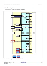
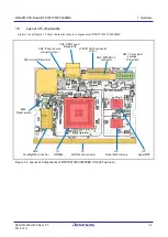
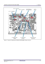
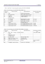
RZ/A2M CPU Board
RTK7921053C00000BE
User's Manual
Renesas Microprocessor
RZ Family / RZ/A Series
User
’
s Ma
nu
al
32
www.renesas.com


