background image

Summary of Contents for cea455 series

Page 1: ...c8 SAMSUNG r z JO t SERVICE MANUAL EGA COLOR MONITOR CEA455 I nil l I L 1 Ir I ...

Page 2: ...ORIZONTAL VERTICAL DEFLECTION 3 POWER SUPPLY DISASSEMBLY INSTRUCTION 11 ALIGNMENT INSTRUCTION 12 TRUOBLESHOOTING GUIDE 16 WIRING DIAGRAM AND PARTS LIST 21 EXPLODED VIEW 29 EXPLODED VIEW PARTS LIST 31 ELECTRICAL PARTS LIST 33 SCHEMATIC DIAGRAM AND WAVE FORM 48 SEMICONDUCTOR LEAD IDENTIFiCATION 50 1 ...

Page 3: ...vel Positive MODE 1 H V Sync TIL Level Positive MODE 2 H Sync TIL Level Positive V Sync TIL Level Negative MODE 1 eGA 640 dots x 200 lines 16 COIOiS MODE 2 EGA 640 dots x 350 lines 64 colors MODE 1 15 75KHz overscan MODE 2 21 8KHz undescan 50Hz 60Hz 9 84 x 6 77 250mm x 172mm 7 MAX 22kV LIMIT 2 4V 5 0Vpp O 3KHz O 3KHz 4 2mm O 5kV NOTES Nominal specs represent the design specs all units should be ab...

Page 4: ... when high voltage is excessive that X radiation is capable of penetrating the shell of the picture tube including the lead in glass material The important precaution is to keep the high voltage below the maximum level specified 2 It is essential that servicemen have available at all times an accurate high voltage meter The calibration of this meter should be checked periodically 3 High voltage sh...

Page 5: ...etal cabinet screw heads knobs and shafts escutcheon etc and measure the AC voltage drop across the resistor Any reading of O 3volt RMS this corresponds to 0 5milliamp AC or more is excessive and indicates a potential shock hazard which must be corrected before returning the display monitor to the user SAFETY NOTICE Many electrical and mechanical parts which have special characteristics in this ch...

Page 6: ...ing Primary signals R G B and secondary signals r g b are mixed through R121 and D116 R123 and D117 R125 and D115 respectively in mode 2 Then the signals are applied to the base of pre amp transistors 0103 0104 0105 The output signals of IC101 in MODE 1 and MODE 2 are selected by the MODE signal from pin no 8 of IC101 SL205 2 VIDEO R G B OUTPUT The R G B drive system is utilized in the video outpu...

Page 7: ...the drive and output stage is a reverse polarity type and that s done when the drive transistor 0401 is on and the output transistor 0402 is off HORIZONTAL OUTPUT AND HV RECTIFIER Horizontal drive voltage which developed at pin 12 of the deflection processor IC401 is amplified through the horizontal drive stage 0401 and coupled to the base of the horizontal output cicuit via the horizontal drive t...

Page 8: ...DE 2 OFF FIG 4 EQUIVALENT CIRCUIT OF HORIZONTAL OUTPUT CIRCUIT TO DY I C414 RL401 J RELAY C416 I T403l11 lrl f TO CRT ANODE I II I II Iii II TO CRT FOCUS TO CRT SCREEN I II I I II II I I 18 l l TO AB L CIRCU IT I II I II II 1 II L I II I 51 II 3 I 19 1 6 0 v TO X RAY PROTECTOR CIRCUIT 145V I I FBT B F b __ E i 2 51 II 5 14 L ___ J L 34V 5V FIG 5 HORIZONTAL OUTPUT AND HV RECTIFIER CIRCUIT 7 ...

Page 9: ...s positively feedback to the base of the output tran sistor included in 1C601 to increase the base current of this transistor As a result of this base current the collector current of that transistor is increased The above operation occurs instaneously to impress suffiecient base current The small signal transis tor 0601 protects 1C601 from the surge current and 0602 is trigger transistor The FBT ...

Page 10: ... 1 V H Al TAC250V L602lliJd LI N 56K 680 FO 6U 2W II t lC6 1 0 6 2 o6 tl7R616 5 7812 L606 f _ t t W v Q o6I j4 1 N QU 90 12V R6qj EUIZ RU 2 fU l 33UH C409 10K II 11 qZ 470U z IOOOU 25V 16V VR601 R617C631 810K 68 470 11 0616 L607 10 1 b l R 2 100UH 99 r FBT B 3 2 le601 STR53041 I A STR54041 cJJ 5 t l FILTEr r 4 P U r T FUSE C603 R OI AC250V 1 F601 i 1p rcm lqjj I 6 1 R60 n1616 L t lKV R618RG 2 z So...

Page 11: ... VERT OSC VERT OUTPUT DY IC102 H SYNC VI H 401 HOR OSC IC301 i H JoSI 1 MODE CONTROL MODE SELECT S W HOR DRIVE SPCT H WIDTH CGA OV IC402 Q401 T401 T402 VR305 fr EGA 3 5V Q302 Q303 H LIN cd C A CkEGA H POSI V SIZE H HOLD HOR OUTPUT Q402 FBT RELAY DRIVE RELAY T403 r Q403 Q404 RL401 IDC 65V EGA r I IDC 54V CGA f i DC 90V f i DC 24V LINE FILTER i RECTIFIER f i POWER SWITCHING SMPS TRANS f i DC 12V L60...

Page 12: ...ove the CRT s anode cap 2 from the CRT 2 Remove the CRT PCB after disconnecting the ground connector 3 Disconnect all of the connectors from the PCBs 4 Remove the main PCB and LED PCB from the front cabinet NOTE Refer to the EXPLODED VIEW for a more detailed disassembly procedure 11 ...

Page 13: ...HOLD MODE1 MODE2 H POSI MODE 1 V SIZE MODE 1 FBT B ADJUSTMENT SIDE PINCUSHION V POSI MODE1 MODE2 H WIDTH COIL H LINEARITY COIL B CUTOFF NO 10 11 12 13 14 15 16 17 12 CRT PCB 151617151 EBEBEBE BACK CONTROL PCB REF NO CONTROL FUNCTION VR103 R CUTOFF VR104 G CUTOFF VR102 B DRIVE VR101 R DRIVE VR 110 SUB BRIGHT VR301 V SIZE MODE 2 VR302 V HOLD MODE1 MODE2 VR303 H POSI MODE 2 ...

Page 14: ...cy at 46Hz 1 1 Hz 2 4 H LINEARITY ADJUSTMENT a Connect the signal cable b Adjust L403 to the optimum linearity in MODE 1 and MODE 2 linearity pattern 13 2 5 H POSITION a Adjust H CENTER VR VR407 to the center of the picture when the signal of MODE 2 is applied b Change mode to CGA MODE MODE 1 15 75KHz and adjust H CENTER VR using CGA H POSI VR VR403 2 6 SIDE PINCUSHION Adjust the side pincushion t...

Page 15: ...rosshatch pattern on the center of the CRT screen FIG 9 KlRIZONTAL 12 LINES MIN VERTICALI 16 LINES MIN FIGURE 9 CROSSHATa t PATTERN Proceed as follows b 1 Locate the pair of four pole magnet rings Rotate the individual rings change spac 14 ing between tabs to convergence the vertical RED and BLUE lines Rotate the pair of rings maintaining spacing be tween tabs to converge the horizontal RED and BL...

Page 16: ...he mis convergence illustrated in FIG 12 has been corrected d Tilt the deflection yoke right and left Insert tilt adjustment wedge 3 between the deflec tion yoke and the CRT until the misconver gence illustrated in FIG 13 has been corrected e Alternately change the spacing between and depth of insertion of the three wedge until proper dynamic convergence is obtained f Check purity and readjust if ...

Page 17: ...C Operation H DEF HV Current Refer to ATT 2 YES Check Vertical NO Check SW301 1C401 Circuit 1C402 1C301 and its related circuit YES Check CRT Socket B NO Check CRT SOcket B Line 145V 85V 6 3V 12V 5V and its related circuit YES Check Self Raster NO disconnect signal cable Check Blanking Circuit YES YES I NO I Check IC101 IC102 Q103 Q105 ZD401 Q405 and Q109 Q114 CRT Pin Connection its related Circui...

Page 18: ...cuit Operation and Signal Cable Refer to An 4 YES Check 16 Color MODE1 or NO Check IC101 IC102 0103 0105 64 Color MODE 2 0109 0114 CRT Pin Connection NO ZD401 0405 and its related Circuit YES Check the BRT and CONT NO I I Operation Check 0101 0102 0106 17 ...

Page 19: ...2V ATT 2 ABNORMAL H OSC H and V CIRCUIT NO RASTER ABNORMAL PICTURE SIZE ABNORMAL VIDEO ON THE SCREEN Check HV X RAY Protector for operation YES The High Voltage Protector Circuitry make an audibole noise during operation when power S W is ON OFF Open the D401 NO Check 1C401 IC402 0401 T401 and its related circuit YES Check the H OSC YES Check H SYNC YES Check ZD401 D406 T403 FBT and its related ci...

Page 20: ... YES NO Check Check Check Check 1C401 IC402 1C401 1C402 IC102 C401 IC401 IC402 VR405 Q401 VR405 NO Check MODE Detector circuit Check V SYNC but H SYNC is normal Vertical adjustment is not possible at all Check IC1 02 IC401 IC301 IC402 SW301 and related circuit 19 Check the Signal Cable connection But Hori SYNC is normal The V SYNC frequency can be varied y slightl Chec IC301 k VR306 C301 C302 IC10...

Page 21: ... SYNC Positive Is the H SYNC positive Is the V SYNC negative pin 6 of IC102 Is the MO negative Is the V SYNC positive pin 11 of IC102 Is the MO positive pin 8 of IC101 YES Check IC102 IC101 and YES its related circuit NO Is the 9 10 11 of 1C402 12V Is the 9 10 11 of 1C402 OV I YES Check Q606 pin 7 of 1C402 5V YES NO Is the FBT B 54V I Is the FBT B 65V YES Check Q603 Q604 Q402 T403 FBT YES NO Does ...

Page 22: ...l v 0 Q113 IINCa COIL _ g I 1 L t 1 1 lCloa CY J ICIOI CN40R 1401 T CRT SOOKET I c I CNJOI5 I LUJ 1111 III IT CNIOC r O QIII07 I j CN301 0 r V rlQ o 109 r n 0 T 8 lb ICI03 LED CNIOJ I CRT 1CN10I C610 IC30 I I J HEA fER lC601 CN603 r NIM POWER DEGAUSSING CN604 F601 JeHIO SWITCH o 0 DEOAUI III Ilr POWER CCRO BOTTCJ4 111 aoTTOM BOTTa l GlROUNJ ROUND QROUNJ 21 22 ...

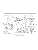
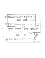
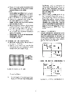
Page 23: ...MAIN PCB TOP VIEW 23 24 ...

Page 24: ...MAIN PCB BOTTOM VIEW 25 26 ...

Page 25: ...LED PCB TOP VIEW CRT PCB TOP VIEW LED PCB BOTTOM VIEW 27 CRT PCB BOTTOM VIEW BACK CONTROL PCB TOP VIEW 28 BACK CONTROL PCB BOTTOM VIEW ...

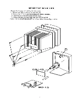
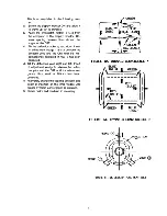
Page 26: ...EXPLODED VIEW 29 ...

Page 27: ... 4 4 I 8 2 2 2 I I 3 3 3 I I I 3 I NO DESCRIPTION SPECIFICATION CODE NO a I TYREMARKS 34 SCREW RH 3XI0 FE FlY 35 HEAT SINK IC AI050S HI4 T2 0 36 TERMINAL BOARD PPO VO 70805 37 SHIELD REAR SECC I TO 5 38 SCREW TAP RH 2S 3XI0 FE FlY 39 SCREW TAP TH 2S 4XI6 FE FlW 40 COVER REAR PPO VO BGE 70805 41 LABEL RATING POLYESTER TO I 42 SCREW TAP FH 2S 4XI5 FE FlW 43 SHIELD TOP SBC I FlW TO 5 44 SCREW TAP RH ...

Page 28: ... METAL FILM RM 1 8T 1K J 01048 177 102 R112 R METAL FILM RM 1 8T 2 7K J 01048 177 272 R114 R METAL FILM RM 1 8T 10K J 01048 177 103 R115 R METAL FILM RM 1 8T 560 J 01048 177 561 R116 R METAL FILM RM 1 8T 560 J 01048 177 561 R117 R METAL FILM RM 1 8T 560 J 01048 177 561 R118 R METAL FILM RM 1 8T 560 J 01048 177 561 R119 R METAL FILM RM 1 8T 560 J 01048 177 561 R120 R METAL FILM RM 1 8T 560 J 01 048...

Page 29: ...R METAL FILM RM 1 ST 1K J 0104S 177 102 R151 R METAL OXIDE RS 2P 56 J S 010S5 527 560 R155 R METAL FILM RM 1 ST 3 3K J 01 048 177 332 R156 R METAL FILM RM 1 8T 2 7K J 01 048 177 272 R161 R CARBON RD 1 4T 120 J 01018 277 121 R164 R CEMENT WIRE RW 3P 1 8K J 01 039 427 182 R165 R CARBON RD 1 4T 22K J 01018 277 223 R166 R CARBON RD l 4T 270K J 01018 277 274 R167 R COMPOSITION RC 1 2T 330 K 01028 378 3...

Page 30: ...018 277 103 R321 R CARBON RD 1 4T 100K J 01018 277 104 R322 R CARBON RD 1 4T 8 2K J 01018 277 822 R323 R CARBON RD 1 4T 1K J 01018 277 102 R324 R CARBON RD 1 4T 220 J 01018 277 221 R325 R CARBON RD 1 4T 5 6K J 01018 277 562 R326 R CARBON RD 1 4T 22K J 01018 277 223 R327 R CARBON RD 1 4T 150 J 01018 277 151 R333 R CARBON RD 1 4T 120 J 01018 277 121 R337 R CARBON RD 1 2T 150 J S 01016 377 151 R341 R...

Page 31: ...N RD 1 4T 220K J 01018 277 224 R422 R CARBON RD 1 4T 2 7K J 01 018 277 272 R423 R CARBON RD 1 4T 6 8K J 01018 277 682 R424 R CARBON RD 1 4T 1 5K J 01018 277 152 R426 R CARBON RD 1 4T 4 7 J 01018 277 479 R427 R CARBON RD 1 4T 1M J 01018 277 105 R428 R METAL OXIDE RS 2P 270 J 01045 527 271 R429 R CARBON RD 1 4T 1K J 01018 277 102 R430 R CARBON RD 1 4T 180K J 01018 277 184 R431 R CARBON RD 1 4T 1K J ...

Page 32: ...S 1P 68 J 01045 427 680 R615 R METAL OXIDE RS 1P 68 J 01045 427 680 R617 R METAL OXIDE RS 1P 68 J 01045 427 680 R618 R METAL OXIDE RS 1P 68 J 01045 427 680 R619 R CARBON RD 1 4T 560K J 01018 277 564 R620 R METAL OXIDE RS 2P 5 6K J S 01085 527 562 R621 R CARBON RD 1 4T 18K J 01018 277 183 R624 R CARBON RD 1 4T 1 8K J 01018 277 182 R627 R CARBON RD 1 4T 100 J 01018 277 101 R633 R CARBON RD 1 4T 1K J...

Page 33: ...270 0409 DIODE 1N4148 T 02169 301 417 0428 DIODE TVR 06G 02169 302 060 0601 DIODE BY133 02169 306 430 0602 DIOQE BY133 02169 306 430 0603 DIODt BY133 02169 306 430 0604 DIODE BY133 02169 306 430 0605 DIODE EU1Z 02169 304 260 0606 DIODE SI RU1 P 02169 206 240 0607 DIODE EU1Z 02169 304 260 0608 DIODE 1N4148 T 02169 301 417 0609 DIODE RGP10G T 02169 219 107 0610 DIODE EU1Z 02169 304 260 0611 DIODE RU...

Page 34: ...2169 404 767 Z0601 0IOOE ZENER UZ 12BM 11 6 12 4 T 02169 404 677 LEO LEO KLG208E 02309 110 090 INTEGRATED CIRCUITS IC101 IC GATE SL205 02109 301 540 IC102 IC KS74HCTLS86 021 09 1 04 700 IC103 IC TTL SN74LS07 02109 101 880 IC301 IC LA7830 02119 101 490 1C401 IC LA7851 02119 101 080 1C402 IC CMOS 14053B MOTOROLA 02109 104 120 1C601 SEE TABLE 1 ON THE PAGE 1C602 IC REGULATOR MC7812C SST 02119 601 700...

Page 35: ...139 302 247 0601 TRANSISTOR KSC2383 T 0602 TRANSISTOR MPSA42 02139 204 030 0603 TRANSISTOR KSB546 Y SST 02149 201 470 0604 TRANSISTOR KSC2310 T 02139 302 247 0606 TRANSISTOR KSC945 Y T 02139 302 747 VARIABLE RESISTORS VR305 VR SEMI CET 92A B500 01241 108 002 VR306 VR SEMI CET 92A B3K 01241 108 005 VR601 VR SEMI CET 92A B10K 01241 108 007 VR402 VR SEMI CET 117A B500 01241 110 001 VR403 VR SEMI CET ...

Page 36: ...uH 02429 060 510 L400 COIL CHOKE 1 MH 02429 060 310 L401 COIL PEAKING 2 7uH 02429 855 210 L402 COIL WIDTH 32uH 40 CEA4551 02449 435 410 H WIDTH COIL L403 COIL H UNEARITY 45uH 02449 734 210 H LiNEARITY L601 SEE TABLE 1 ON THE PAGE L602 SEE TABLE 1 ON THE PAGE L604 COIL FILTER 33uH 02429 060 510 L606 COIL FILTER 33uH 02429 060 510 L607 COIL CHOKE 100uH K 10 PI N Y 02429 052 020 DEGA COIL DEGAUSSING ...

Page 37: ... COIL CHOKE 1 5uH 20 02429 048 010 FERRITE BEAD CN101 CONNECTOR WAFER 5267 09A MOLEX 03344 156 190 SIGNAL CABLE CN101 SIGNAL CABLE ASSY L1000 CEA4551 03051 401 610 SIGNAL CABLE CN103 CONNECTOR WAFER 5267 04A MOLEX 03344 156 140 BRI CONT LINE CN103 CON 4P ASSY H 5264 04 450MM 03054 646 150 BRI CONT LINE CN107 CONNECTOR WAFER 5267 02A MOLEX 03344 156 120 HEATER LINE HEATER CONN 2P ASSY 5264 02 L 300...

Page 38: ...017 271 C109 C ELECTROLYTIC CE04W T 16V 47M 01608 903 470 C112 C CERAMIC HK CK45 T F 50V 0 1 M Z 01417 344 104 C113 C ELECTROLYTIC CE04W T 16V 100M 01608 903 101 C114 C ELECTROLYTIC CE04W T 16V 10M 01608 903 110 C115 C ELECTROLYTIC CE04W T 16V 22M 01608 903 220 C116 C CERAMIC HK CK45 T F 50V 0 1 M Z 01417 344 104 C117 C CERAMIC HK CK45 T F 50V 0 1 M Z 01417 344 104 C118 C CERAMIC HK CK45 T F 50V 0...

Page 39: ...12 C ELECTROLYTIC CE04W 3SV 100M 01609 402 100 C313 C ELECTROLYTIC CE04W T 2SV 100M 01608 904 101 C31S C ELECTROLYTIC CE04W T 3SV 22M 10S C RA 01607 905 220 C316 C POLYESTER C0921 M T 100V 0 1 M J 01505 723 104 C321 C CERAMIC HK CK4S T B SOOV S60 K 01417 468 561 C322 C CERAMIC HK CK4S T B SOOV 100 K 01417 468 101 C326 C POLYESTER C0921M T 100V 0 047 J 01505 723 473 C329 C CERAMIC HK CK4S T B SOV 1...

Page 40: ...C CERAMIC HK CK45 T B 500V 100 K 01417 468 101 C430 C ELECTROLYTIC CE04W T 10V 47M 01608 902 470 C435 C POLYESTER CQ921M T 100V O 1 J 01505 723 1 04 C437 C POLYESTER CQ921 M T 100V 0 0022 J 01505 723 222 C438 C ELECTROLYTIC CE04W 16V 220M 01609 401 482 C600 SEE TABLE 1 ON THE PAGE C601 C CERAMIC AC CK45B 250V 2200 M 01461 136 806 C602 C CERAMIC AC CK45B 250V 2200 M 01461 136 806 C603 C M POLYESTER...

Page 41: ...1603 905 222 C625 C CERAMIC HK CK458 1KV 470 01419 901 090 C626 C ELECTROLYTIC CE04W 16V 1000M 01609 401 510 C629 C ELECTROLYTIC VENT CE04W 25V 470M 13x20 01603 904 471 C631 C CERAMIC HK CK458 1KV 470 01419 901 090 C632 C ELECTROLYTIC CE04W 100V 220M 01609 403 120 C634 C CERAMIC HK CK458 1KV 470 01419 901 090 C635 C ELECTROLYTIC CE04W 100V 220M 01609 403 120 C637 C CERAMIC HK DE7150F 472M VA 1 KC ...

Page 42: ...5 040 PTH451C06BG08ON14O 02199 003 120 PTH451C02BG200N270 IC601 IC 02119 601 540 STR53041 02119 601 660 STR54041 C600 C CERAMIC HK 01416 768 472 CK45B 2KV 4700 K TABLE2 CRT LIST FOR MODEL NO MODEL NO CODE NO SPECIFICATION REMARK CEA4551 02019 234 310 3709B22 ST TC09 0 31NG CEA4552 02019 237 510 37GGA44X TC01 0 39G CEA4553 02019 237 610 37SGA44X TC01 0 39NG CEA4554 02019 237 810 37GGA54X TC10 0 41G...

Page 43: ...FABRICANT DONT LE FONCTIONNEMENT EST CRITITE QUE PAR OES PIECES RECOMMANDEES PAR LE FABRICANT CONSULTER LA NOMENCLA TURE DES PIECES POUR TROUVEA LES PIECES DE RECHANGE EXACTES RESISTANCE IS SHOWN IN K 1 000 M 1 000 000 RATED POWER OF RESISTOR NOT NOTED IN SCHEMATIC DIAGRAM IS 1 4 2 CAPACITANCE IS SHOWN UFo AND NOT NOTED CAPACITANCES IS SHOWN PF tUF 1 000 OOOPF RATED VOLTAGE OF CAPACITOR NOT NOTED ...

Page 44: ...C1507 0109 0111 1 16 0113 0401 MC14053B KSB546 Y 0603 SL205 KSA614 Y 0303 1 14 2SD1555 SN7407 2SD1879 0402 2SD1556 STR53041 STR54041 2N3904 KSC945 KSC1008 74HCTLS86N 1C601 If 0 LA7830 1234567 0103 0104 1 O 0105 0110 0112 0114 0302 0403 LA7851 0405 0606 0101 0102 0404 KSA733 0106 50 REF NO 1C602 1C402 IC101 IC103 IC102 IC301 IC401 ...

Page 45: ...MEMO 51 ...

Page 46: ......

Page 47: ...PRINTED IN KOREA CODE NO 08147 400 110 ...

Reviews: