background image

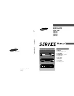
DVD PLAYER

Chassis : Sellino
DVD-S221
DVD-S222
DVD-S320
DVD-S321

SERVICE 

1. Precautions

2. Disassembly and Reassembly

3. Troubleshooting

4. Exploded Views and Parts List

5. Electrical Parts List

6. Block Diagrams

7. PCB Diagrams

8. Wiring Diagrams

9. Schematic Diagrams

Manual 

DVD PLAYER

CONTENTS

SERVICE MANUAL

DVD-S221/S222/S320/S321

OPEN/CLOSE

OPEN/CLOSE

STOP

PLAY/PAUSE

OPEN/CLOSE

/ SHUTTLE

SKIP

DVD-S221

DVD-S220/S320

DVD-S321

ELECTRONICS

© Samsung Electronics Co., Ltd. 

DEC. 2001

Printed in Korea

AH82-00117A

Summary of Contents for DVD-S221

Page 1: ...s and Parts List 5 Electrical Parts List 6 Block Diagrams 7 PCB Diagrams 8 Wiring Diagrams 9 Schematic Diagrams Manual DVD PLAYER CONTENTS SERVICE MANUAL DVD S221 S222 S320 S321 OPEN CLOSE OPEN CLOSE STOP PLAY PAUSE OPEN CLOSE SHUTTLE SKIP DVD S221 DVD S220 S320 DVD S321 ELECTRONICS Samsung Electronics Co Ltd DEC 2001 Printed in Korea AH82 00117A ...

Page 2: ...rwriters Laboratories UL 1270 40 7 With the instrument s AC switch first in the ON position and then in the OFF position measure from a known earth ground metal water pipe conduit etc to all exposed metal parts of the instrument antennas handle brackets metal cabinets screw heads metallic overlays control shafts etc espe cially any exposed metal parts that offer an electri cal return path to the c...

Page 3: ...ched out of place or frayed wiring Do not change spacing between a component and the printed circuit board Check the AC power cord for damage 5 Components parts and or wiring that appear to have overheated or that are otherwise damaged should be replaced with components parts and or wiring that meet original specifications Additionally determine the cause of overheating and or damage and if necess...

Page 4: ...nd lead last 2 The service precautions are indicated or printed on the cabinet chassis or components When servic ing follow the printed or indicated service precau tions and service materials 3 The components used in the unit have a specified flame resistance and dielectric strength When replacing components use components which have the same ratings Components i enti fied by shading by or by in t...

Page 5: ...posure of the assem bly 3 Use only a grounded tip soldering iron to solder or unsolder ESD devices 4 Use only an anti static solder removal devices Some solder removal devices not classified as anti static can generate electrical charges suffi cient to damage ESD devices 5 Do not use freon propelled chemicals These can generate electrical charges sufficient to damage ESD devices 6 Do not remove a ...

Page 6: ... sheet This gives them the same ground as the sheet 4 Remove the optical pick up block 5 Perform work on top of the conductive sheet Be careful not to let your clothes or any other static sources to touch the unit Be sure to put on a wrist strap grounded to the sheet Be sure to lay a conductive sheet made of copper etc Which is grounded to the table Fig 1 3 6 Short the short terminal on the PCB wh...

Page 7: ... Assy 3 Make solder land 2 points short on Pick up See Fig 1 4 4 Disassembly the Pick up 1 5 2 Assembly 1 Replace the Pick up 2 Remove the soldering 2 points on Pick up 3 Reassemble the Deck Assy SOLDER LAND 2 POINTS SHORT PICK UP ASS Y Note If the assembly and disassembly are not done in correct sequence the Pick up may be damaged Fig 1 4 ...

Page 8: ...ssembly and Reassembly 2 1 Cabinet and PCB 2 1 1 Top Cabinet Removal 1 Remove 3 Screws Œ on the back Top Cabinet 2 Lift up the Top Cabinet in direction of arrow Œ 3 SCREWS Fig 2 1 Top Cabinet Removal Note Reassembly in reverse order ...

Page 9: ...he Door Tray in direction of arrow A 3 Close Tray Œ and power off Note If Tray Œ doesn t open insert a Screw driver into the Emergency hole ˇ as shown in detailed draw ing and then push it in the direction of arrow B Open Tray manually Side View ˇ EMERGENCY HOLE SCREW DRIVER B Œ TRAY DOOR TRAY A Fig 2 2 Door Tray Removal ...

Page 10: ...Cabinet Removal DVD S221 S222 S320 2 1 3 Ass y Front Cabinet Removal DVD S221 S222 S320 1 Release 6 Hooks Œ ˇ and remove Ass y Front Cabinet ˆ DVD S321 1 Remove Knob Volume Œ 2 Release 6 Hooks ˇ ˆ and remove Ass y Front Cabinet Ø 3 Remove Knob Jog 5 Screws and Key PCB Fig 2 4 Ass y Front Cabinet Removal DVD S321 2 HOOKS Œ 2 HOOKS ˆ ASS Y FRONT CABINET ˇ 1 HOOK 1 HOOK ...

Page 11: ...y DECK ASS Y Œ 3 SCREWS DCN1 DCN2 DCN3 FLAT CABLE CONNECT WIRE MAIN PCB 2 1 4 Ass y Deck Removal 1 Disconnect Flat Cable Connect Wire from DCN1 DCN2 and DCN3 on Main PCB 2 Remove 3 Screws Œ from the Ass y Deck and lift it up Fig 2 5 Ass y Deck Removal ...

Page 12: ...amsung Electronics 2 5 ˆ MAIN PCB 3 SCREWS 1 SCREW Œ 2 SCREWS ˇ JACK PCB Fig 2 6 Main PCB Jack PCB Removal 2 1 5 Main PCB Jack PCB Removal 1 Remove 3 Screws Œ and lift up the Jack PCB ˇ 2 Remove 3 Screws and lift up the Main PCB ˆ ...

Page 13: ...2 6 Samsung Electronics Disassembly and Reaasembly JACK PCB MAIN PCB DVD S221 S222 S320 DVD S321 JACK PCB MAIN PCB KEY PCB 2 2 PCB Location Fig 2 7 PCB Location ...

Page 14: ...ECK ASS Y MAIN PCB DCN1 ˇ FLAT CABLE DECK ASS Y MAIN PCB DCN2 ˆ CONNECT WIRE HCN1 HOUSING PCB JACK PCB DCN3 Ø CN8 MAIN PCB JACK PCB CN1 PCN1 MAIN PCB JACK PCB PCNS1 CT1 CT2 CT3 CT4 CT5 DVD S221 S222 S320 Œ ˇ ˆ Ø CT1 CT3 CT2 DECK ASS Y JACK PCB MAIN PCB CT4 CT5 2 3 Connector Diagram Fig 2 8 Connector Diagram ...

Page 15: ... Y MAIN PCB DCN1 ˇ FLAT CABLE DECK ASS Y MAIN PCB DCN2 ˆ CONNECT WIRE HCN1 HOUSING PCB JACK PCB DCN3 Ø CN8 MAIN PCB JACK PCB CN1 PCN1 MAIN PCB JACK PCB PCNS1 Ô CN3 JACK PCB KEY PCB KCN1 CT1 CT2 CT3 CT4 CT5 CT5 DVD S321 Œ ˇ ˆ Ø Ô CT1 CT3 CT2 DECK ASS Y JACK PCB MAIN PCB KEY PCB CT4 CT5 CT6 Fig 2 9 Connector Diagram ...

Page 16: ...der Housing ˇ in the direction arrow A 2 When the Tray Disc comes out a little pull it in the direction arrow B by hand 3 Pull the Tray Disc to disassemble while simultaneously pushing 2 Stoppers ˆ left right in the direction arrow C D Fig 2 10 Tray Disc Removal A Œ SCREW DRIVER EMERGENCY HOLE ˇ SLIDER HOUSING TRAY DISC B C ˆ STOPPER ˆ STOPPER D ...

Page 17: ...4 2 Assy P U Deck Removal 1 Disconnect DCN2 Œ DCN3 2 Lift down the Assy P U Deck ˇ while simultaneously pushing 2 Hooks ˆ in the direction of arrow A B Fig 2 11 Assy P U Deck Removal Œ DCN2 ˆ HOOK HOOK DCN3 ˇ ASSY P U DECK A B Assembly Point SLIDER HOUSING ...

Page 18: ... Gear Tray 4 Lift up the Slider Housing ˆ 5 Remove the soldering Ø of 2 points Red Black 6 Remove 2 Screws and lift down the Motor Load Assy 7 Push the 3 Hooks bottom side in the direction arrow C and lift up the Housing PCB 8 Push the Hooks Ô and remove Deck PCB Fig 2 12 Housing Ass y Removal Œ BELT ˇ PULLEY GEAR GEAR TRAY MOTOR LOAD ASSY 3 HOOKS HOUSING PCB Ô HOOK Ø SOLDERING 2 SCREWS ˆ SLIDER H...

Page 19: ...sembly and Reaasembly 2 4 4 Sub Chassis Removal 1 Remove the Soldering of Motor Feed wire Œ 2 Remove the 4 Screws 3 Lift up the Ass y Brkt Deck ˇ Fig 2 13 Sub Chassis Removal 4 SCREWS ˇ ASSY BRAK DECK Œ SOLDERING OF MOTOR FEED WIRE ...

Page 20: ...d B Gear Feed A ˇ 3 Remove 2 Screws 4 Remove Shaft Pick Up ˆ and Pick Up Assy Ø 5 Remove 1 Screw 6 Remove 2 Screws 7 Remove 3 Spring Spindle and Motor Spindle Ass y Fig 2 14 Ass y Brkt Deck Removal 2 SCREW Œ WASHER GEAR FEED B 2 SCREWS 1 SCREW ˆ SHAFT PICK UP ˇ GEAR FEED A Ø PICK UP ASS Y SPRING SPINDLE MOTOR SPINDLE ...

Page 21: ...2 14 Samsung Electronics Disassembly and Reaasembly MEMO ...

Page 22: ...tputted from object lens at play key input No focus incoming and no disc occurs Yes No B A No focus incoming FE in SIC1 25 is within specified range SIC3 26 27 output are normal Check open state from SIC3 to pick up Check RIC1 and A B C D input Check SIC3 Yes Yes No No A ...

Page 23: ... Motor and connection Check MIC1 Yes No SLED SLED SIC3 32 33 output are normal Check SIC3 Yes No NO LD CD ON RIC1 19 is 5V Current exceeds 0 1A LD out pick up replace Open check in related circuit Check MIC1 Yes Yes Yes No No Divide RQ2 emitter terminal voltage and 5V real voltage difference into 10ohm B ...

Page 24: ...Focus On Yes Yes Yes A See Fine Seek Check No Yes Check pick up No FINE SEEK Check FINE SEEK MIRR signal RIC1 65 is missing TZCO signal SIC1 24 is occurs Track incomming is delayed TE is within 2V and 3V Pick up transfer smooth Check RIC1 Peripheral curcuit Check SIC1 Peripheral curcuit Time out due to many jump counts Check SIC1 peripheral circuit SIC1 33 output is normal SIC3 28 29 terminal outp...

Page 25: ...c motor Check SIC1 MIC1 Check SIC3 soldering and power Check path to RIC1 and SIC1 Check RIC1 soldering and power RIC1 70 output are normal RIC1 71 output is normal Check RIC1 peripheral circuit and A B C D Yes Yes Yes Yes Yes Yes No No No No No No No Tray open close MIC1 36 37 is Open L L Close H H Check SIC3 35 36 output at open close Check signal line state from SIC3 35 36 to tray motor Micom M...

Page 26: ...ck ZIC1 121 output Check ZIC1 125 CD VCD 16 9344MHz DVD 18 432MHz Yes Yes No No AOP4 1 7 output is normal Check AOP1 peripheral circuit Yes No Base terminal level of AQ1 AQ3 are L Check FIC1 11 mute Yes No Headphone output error AVJ2 L R output is normal HOP1 1 7 output is normal Check 3 pin Headphone jack peripheral soldering shot Check AVJ2 L R output error Check HOP2 1 7 output Yes No No Yes ...

Page 27: ... ZIC1 peripheral circuit Check AIC3 Yes No No Yes No Power 120 Voltage Standby LED OFF PFD01 error PDS01 voltage is missing Replace PQR11 Replace fuse Check PDS01 04 No No Yes Collector of PQR11 output normal voltage Check 2 d voltage No Operation of PQR11 is normal Replace PQR12 Yes No Switching operation of PQR11 is normal Replace PQR11 Check feed back Yes Yes No Yes ...

Page 28: ...Check the soldering of VSW1 Yes No No FIC1 61 is high state Check the connection between FIC1 61 and VR121 Yes No Yes D Y Pr Pb output error VSW1 video select switch is down position VR121 of VSW1 is low state Move the select switch to down position Check the soldering of VSW1 Yes No No FIC1 61 is high state Check the connection between FIC1 61 and VR121 Yes No Yes D ...

Page 29: ...VIC1 1 34 Yes No Pin 7 in VIC1 is in high stste Yes Check the connection netween pin 133 in ZIC1 and VIC1 Check the connection betwen VIC1 and PICS4 2 Check the connection between PICS4 2 and pin 1 in VIC1 Check the soldering of VIC1 No No Check the connection between VIC1 and output jack Pin of VDD_2 5 VDD 3 3 in Zic1 has normal level Check the connection between pin 1 in PCNS1 and pin 3 in ZIC5 ...

Page 30: ...4 1 4 Exploded View and Parts List 4 1 Cabinet Assembly 4 2 Deck Assembly Page 4 2 4 4 ...

Page 31: ...ervice Not Available DVD S221 DVD S222 S320 DVD S321 UT01 UT02 DVD S221 S222 S320 DVD S321 1 2 1 4 701 151 3 Only for DVD S320 S321 101 151 151 150 601 ASSY PCB MAIN S N A ASS Y CABINET BOTTOM 610 150 13 151 CN1B DECK DVD MECHA S N A 602 ASS Y PCB JACK 1 2 2 12 12 ...

Page 32: ...6003 000276 SCREW TAPTITE BH B M3 L10 ZPC YEL SWC 601 Refer to table below ASSY PCB MAIN DVD S221 XAA MAIN PCB USA 602 Refer to table below ASSY PCB JACK DVD S221 XAA JACK ASS Y U 610 AC39 10200N POWER CORD EP2 SPT 2 AWG 18 1 8MT WAFER CN1B 3809 001180 CABLE FLAT 30V 30to 80C 80mm 35P 1 25mm UT01 Refer to table below REMOCON ASS Y DVD S221 XAA UT02 Refer to table below REMOCON ASS Y DVD S321 XAA O...

Page 33: ...Exploded Views and Parts List 4 4 4 2 Deck Assembly H108 H106 S N A H105 H107 H102 H211 H203 H241 H212 905 H104 H250 H103 H207 H208 S N A H202 H210 H204 H205 H209 H206 901 900 904 906 903 ...

Page 34: ...1 2 4 3 1 2X25 1 B H106 AH66 00124A GEAR TRAY DP 7 POM M90 44 H107 AH66 00125A SLIDER HOUSING DP 7 POM H108 AH63 00217A TRAY DISC ABS BLK DP 7 H202 AH73 00023A RUBBER INSULATOR BUTYL RUBBER DP 3 H203 AH61 50327A SHAFT P U DP 3 SUS420J2 L84 7 OD3 H204 AH66 00075A GEAR FEED A POM M90 44 H205 AH66 00170A GEAR FEED B DP 7S POM M90 44 0 5 14 H206 AC60 30306A WASHER SLIT ID2 1 OD5 0 T0 5 POLYS H207 AH31...

Page 35: ...Exploded Views and Parts List 4 6 MEMO ...

Page 36: ...8 MR23 2007 000090 R CHIP 10KOHM 5 1 16W DA TP 1608 MR25 2007 000090 R CHIP 10KOHM 5 1 16W DA TP 1608 MR26 2007 000084 R CHIP 4 7Kohm 5 1 16W DA TP 1608 MR27 2007 000084 R CHIP 4 7Kohm 5 1 16W DA TP 1608 MR28 2007 000084 R CHIP 4 7Kohm 5 1 16W DA TP 1608 MR29 2007 000084 R CHIP 4 7Kohm 5 1 16W DA TP 1608 MR3 2007 000084 R CHIP 4 7Kohm 5 1 16W DA TP 1608 MR30 2007 000084 R CHIP 4 7Kohm 5 1 16W DA T...

Page 37: ...1 C CERAMIC CHIP 0 027nF 5 50V NP0 TP 160 SC35 2203 000257 C CERAMIC CHIP 10nF 10 50V X7R TP 1608 SC36 2203 000257 C CERAMIC CHIP 10nF 10 50V X7R TP 1608 SC37 2203 000257 C CERAMIC CHIP 10nF 10 50V X7R TP 1608 SC38 2203 000257 C CERAMIC CHIP 10nF 10 50V X7R TP 1608 SC39 2203 000626 C CERAMIC CHIP 0 022nF 5 50V NP0 TP 160 SC40 2203 000626 C CERAMIC CHIP 0 022nF 5 50V NP0 TP 160 SC41 2203 000626 C C...

Page 38: ...50V NP0 TP 160 ZC60 2203 000681 C CERAMIC CHIP 0 027nF 5 50V NP0 TP 160 ZC61 2007 000070 R CHIP 0ohm 5 1 16W DA TP 1608 ZC62 2203 000681 C CERAMIC CHIP 0 027nF 5 50V NP0 TP 160 ZC63 2203 000626 C CERAMIC CHIP 0 022nF 5 50V NP0 TP 160 ZC66 2203 000260 C CERAMIC CHIP 10nF 10 50V X7R TP 2012 ZC67 2203 000260 C CERAMIC CHIP 10nF 10 50V X7R TP 2012 ZC68 2203 000260 C CERAMIC CHIP 10nF 10 50V X7R TP 201...

Page 39: ...7 R CHIP 1 8KOHM 5 1 10W DA TP 2012 AR35 2007 000300 R CHIP 10KOHM 5 1 10W DA TP 2012 AR36 2007 000572 R CHIP 220OHM 5 1 10W DA TP 2012 AR38 2001 000515 R CARBON 220OHM 5 1 8W AA TP 1 8X3 2MM AR4 2001 000290 R CARBON 10KOHM 5 1 8W AA TP 1 8X3 2MM AR40 2001 000429 R CARBON 1KOHM 5 1 8W AA TP 1 8X3 2MM AR403 2007 000468 R CHIP 1KOHM 5 1 10W DA TP 2012 AR404 2007 000468 R CHIP 1KOHM 5 1 10W DA TP 201...

Page 40: ...PEF 100nF 5 50V TP 10X9X4 3X5 5m PDD35 0402 001195 DIODE RECTIFIER F1T4 400V 1 0A TS 1 TP PDR11 0401 000101 DIODE SWITCHING 1N4148 100V 200mA DO 35 PDR12 0401 000101 DIODE SWITCHING 1N4148 100V 200mA DO 35 PDS01 0402 001196 DIODE RECTIFIER 1T5 600V 1A TS 1 TP PDS02 0402 001196 DIODE RECTIFIER 1T5 600V 1A TS 1 TP PDS03 0402 001196 DIODE RECTIFIER 1T5 600V 1A TS 1 TP PDS04 0402 001196 DIODE RECTIFIE...

Page 41: ... 2012 VR13 2001 000969 R CARBON 75OHM 5 1 8W AA TP 1 8X3 2MM VR14 2001 000969 R CARBON 75OHM 5 1 8W AA TP 1 8X3 2MM VR15 2001 000969 R CARBON 75OHM 5 1 8W AA TP 1 8X3 2MM VR16 2001 000969 R CARBON 75OHM 5 1 8W AA TP 1 8X3 2MM VR21 2007 001166 R CHIP 75OHM 5 1 10W DA TP 2012 VR22 2007 001166 R CHIP 75OHM 5 1 10W DA TP 2012 VR24 2007 000029 R CHIP 0OHM 5 1 10W DA TP 2012 VSW1 AH34 00010A SWITCH SLID...

Page 42: ... Yout Cout SIC1 S5L1454A Servo DSP RIC1 S5L1462B RF Amp DPD MIC1 TMP91C829F Main Controller FIC1 GMS81C2020 Front Controller ZIC1 ZiVA 4 1 A V Decoder CVBS Pr Pb Y L R Post Filter Optical A V Decoder AC3 MPEG 2 5 1 CH Video Encoder 4DAC AUDIO DSP CSS INPUT FIFO DEMUX AIC4 PCM1742KE 2 CH Audio DAC Down L R Compo Post Filter Y B Pb Post Filter C R Pr Post Filter Comp G Y IEC958 1937 VIC1 MM1567A MIC...

Page 43: ...ut SIC1 S5L1454A Servo DSP RIC1 S5L1462B RF Amp DPD MIC1 TMP91C829F Main Controller FIC1 GMS81C2020 Front Controller ZIC1 ZiVA 4 1 A V Decoder CVBS Pr Pb Y L R Headphone Post Filter Post Filter Optical A V Decoder AC3 MPEG 2 5 1 CH Video Encoder 4DAC AUDIO DSP CSS INPUT FIFO DEMUX AIC4 PCM1742KE 2 CH Audio DAC Down L R Compo Post Filter Y B Pb Post Filter C R Pr Post Filter Comp G Y IEC958 1937 VI...

Page 44: ...Samsung Electronics 7 1 7 PCB Diagrams 7 2 7 3 7 4 7 1 Main 7 2 Jack 7 3 Key Only for DVD S321 ...

Page 45: ...PCB Diagrams 7 2 Samsung Electronics 7 1 Main COMPONENT SIDE SOLDER SIDE ...

Page 46: ...PCB Diagrams Samsung Electronics 7 3 7 2 Jack ...

Page 47: ...PCB Diagrams 7 4 Samsung Electronics 7 3 Key Only for DVD S321 ...

Page 48: ...Samsung Electronics 8 1 8 Wiring Diagrams 8 1 DVD S221 S222 S320 ...

Page 49: ...Wiring Diagrams 8 2 Samsung Electronics 8 2 DVD S321 ...

Page 50: ...ey 9 3 Servo 9 4 Front Micom VFD Display Only for DVD S221 S222 S320 9 5 Front Micom VFD Display Only for DVD S321 9 6 Video 9 7 Audio Only for DVD S221 S222 S320 9 8 Audio Only for DVD S321 9 9 Headphone Only for DVD S321 9 10 Key Only for DVD S321 Block Identification of PCB Main PCB Component Side Jack PCB Conductor Side ...

Page 51: ...Schematic Diagrams 9 2 Samsung Electronics 9 1 Power ...

Page 52: ...Schematic Diagrams Samsung Electronics 9 3 9 2 AV Decoder Main Micom Key ...

Page 53: ...Schematic Diagrams 9 4 Samsung Electronics 9 3 Servo ...

Page 54: ...Schematic Diagrams Samsung Electronics 9 5 9 4 Front Micom VFD Display Only for DVD S221 S222 S320 ...

Page 55: ...Schematic Diagrams 9 6 Samsung Electronics 9 5 Front Micom VFD Display Only for DVD S321 ...

Page 56: ...Schematic Diagrams Samsung Electronics 9 7 9 6 Video ...

Page 57: ...Schematic Diagrams 9 8 Samsung Electronics 9 7 Audio Only for DVD S221 S222 S320 ...

Page 58: ...Schematic Diagrams Samsung Electronics 9 9 9 8 Audio Only for DVD S321 ...

Page 59: ...Schematic Diagrams 9 10 Samsung Electronics 9 9 Headphone Only for DVD S321 ...

Page 60: ...Schematic Diagrams Samsung Electronics 9 11 9 10 KEY Only for DVD S321 ...

Page 61: ...Schematic Diagrams 9 12 Samsung Electronics MEMO ...

Reviews: