background image

Summary of Contents for ER-3715 Series

Page 1: ...SAMSUNG Electronics SERVICE MANUAL ELECTRONIC CASH REGISTER ER 3715 3615 SERIES CR 802A 812A FRONT 10 REAR 9 Design and specifications are subject to change without notice...

Page 2: ...ME CLOCK CIRCUIT PRINTER CIRCUIT 3 SPECIFICATION OF MAJOR COMPONENT 3 1 3 2 3 3 3 4 CPU PORT DESCRIPTION CR 802A CR 812A PRINTER F P C TERMINAL ARRANGEMENT GENERAL SPECIFICATIONS KA2657 LM339 74HCT138...

Page 3: ...s technical information for many individual component systems circuit and gives an analysis of the operations performed by the circuits Also included is technical information on the EPSON two station...

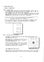
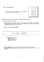
Page 4: ...nd depress the SUBTOTAL key While holding the SUBTOTAL down power the register off and back on The following receipt will be issued aeeeseeres Sete ee RNR RN NS 22009792 o STEP 2 Clearing Totals From...

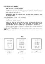
Page 5: ...into the control lock See figure on preceding page and turn clockwise past the position marked P to the Master Clear position This position is not marked on the control lock but the C key can travel...

Page 6: ...he power source Keyboard Test Enter 2 and press the CASH TEND key One at a time press all the keys on the keyboard Each key will show its location code on the display as it is depressed Exit the keybo...

Page 7: ...into the control lock see page 3 and turn clockwise to the Master Clear S Mode position This position is not marked on the control lock and only the key will travel to this position Enter the followi...

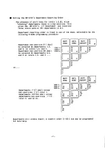
Page 8: ...position 1 shall be occupied by departments 1 2 veueta and 3 on levels 1 2 and 3 LEVEL 2 Department key position 2 shall ever3 be occupied by departments 4 5 and 6 on levels 1 2 and 3 55 65 56 86 10...

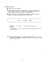
Page 9: ...position Enter the digit for desired department assignment order see below press the X TIME key followed by the CASH key 0 OR 1 X TIME CASH 0 level 1 1 117 level 2 118 234 level 3 235 351 DEFAULT 1 K...

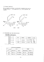
Page 10: ...ven Membrane Membrane sheet MAIN PCB TR MAIN PCB a Lower case good Lower case bad a b SIDE VIEW 1 3 TRANSFORMER AND FUSE SPECIFICATION TRANSFORMER _SPECIFICATION EUROPE men PRIMARY SECONDARY U S A S A...

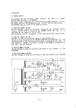
Page 11: ...DGE DIODE BD2 and it is regulated by the capacitor 4700 pF CEZ The switching circuit is composed of two transistors and a zener diode 2 VCC 5V MARK E ON PCB The VCC is used for the power source of the...

Page 12: ...VBT pg EK 04 220 R30 RTC VBT MARK F ON PCB 3 6V oe 2 3 RESET AND POWER FAIL DETECTION CIRCUIT The reset circuit prevents the CPU from starting to operate before the system is fully powered up and init...

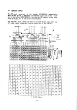
Page 13: ...tascos L rrecos rr2cos ag 34668 7 i 8 seae of n su14830 Fi 16 4913yq Oi ea eee a eh Lega he Lgg74 a 9574 25456789 442534867606 12348567869 072103466 OBB430 27 O76254403 2 5 DRAWER AND BUZZER CIRCUIT...

Page 14: ...7hoshisahiowbeslis7f aah eueeEEEeouaaaee ee 1 a 2 a feo okoshacks e ae Peerceenmiarieeest 7 38 2a 31 30 47 s6 esooksahsohe7hkaskas 84Hoa s2heojee hssel44 2 8 8 EIE ce 7 ta _ h BS lop on RSoO as iz ts...

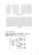
Page 15: ...e clock circuit is composed of a timer IC19 RP5C15 two capacitors The CPU reads a time data from RP5C15 and writes a new time data to the RP5SC15 The address line means the content of the secs mins ho...

Page 16: ...on of the character wheel The CPU detects the timing pulse compares the pulse count and the data for printing If the count meets the data the CPU sends a high Signal to the LATCH IC 74HCT574 during th...

Page 17: ...DDRESS DATA BUS q 5 w w e cod wo i e e m o EH Ce ee 70 S DAT CLOCK CHIP sasct o P1 6 34 Po5 AD5 ee ee 1 reser 9 32 po7 ap7 ADDRESS DATA BUS is 0 ADDRESS LATCH INTO PGM STORE ENABLE INT1 3 28 7 AD15 1...

Page 18: ...ependent paper feeding of receipts and journals and quick feeding of receipts are possible 2 Stamp print and validation print can be conducted 3 Inking system using ink rollers 4 Validation sensor is...

Page 19: ...UD VY YOOUYY stances ah ea fs ee AHHH O common wire is Motor ig R side trigger magnet unit common wire 20 aE R side trigger magnet unit column No 1 BO TT R side trigger magnet unit column No 2 ite OKT...

Page 20: ...S ENABLE SELECT Y4 Y5 Y6 Y7 3 OR ai De G2A GzB i ENABLE d INPUTS s DATA QUTPUTS SELECT INPUTS CRP Rr Rm Corer xe Ss bp eee Cees ERO OEE ce co ea et GR da i Ce Ee our oo XS Gor Lore Le Lor x xX po ne C...

Page 21: ...4LS573 i um tM on oe S ay BS Oo oa Q no wee FUNCTION TABLE LS574 Qo a Tw 16 15 14 A 0C ENABLE C aon on wo Gc 1312 41 FUNCTION TABLE LS541 _ e 2 oO 2 OUT2 OUT4 IN4 OUTS INS LOGIC DIAGRAM OUT6 IN6 6 NC...

Page 22: ...5 WOs VO4 N C vec asa A w a7 ce2 AG a8 AS ag AA AML Aa 0 A2 AiO AL cei 40 1 08 1 01 1 07 1 02 1 06 1 03 1 05 6NO 1 04 21 SRAM 62256 32K x 8 PIN FUNCTION CHIP ENABLE 1 O 1 08 SRAM 6264 8K ADDRESS INPUT...

Page 23: ...010RB6 FGSTG Less e See 11 aves eo 22 24 FGIO1ORBG 1 12 13 FG97D6 17 GRID 1 18 PLATE COM 19 PLATE d 20 PLATE dp 21 PLATE c 22 PLATE b 23 PLATE a 24 FILAMENT FG1010RB6 PIN ASSIGNMENT rs rR 21 PLATE a 2...

Page 24: ...4 GENERAL OVERVIEW SYSTEM BLOCK DIAGRAM POWER FAIL INTO lo OISPLAY 23 DOTSPLAY KEY BOARO...

Page 25: ...MAIN PCB LAYOUT NOULISIOP E3NI7 LNO NOHLIOIG ziWo ONNSHUS ging 1047ER3715 S04 836 COMP REV MD 92 2 15 24...

Page 26: ...PRINTER 6 PIN 60 KEY SCAN 42 PIN 90 KEY SCAN 20 PIN 460 KEY SCAN CN10 KEY BOARD SCAN 8 12 20 PIN CN3 STANOARD DRAKER CN4 MULTI DAAWEAR CNA MULTI COMPULSORY _ ap STANDARO COMPULSORY 2 POWER TRANS CNS F...

Page 27: ...y OO a Lary a ee a OO 2 meee a Ce Os o i t 3e Oo 30 ty t e xD ve se se re ee GOdcHI 631 tS et EF Pt ST SF a Co ET ET we of al of s ef ed vl ol ol clad 1 alchaie ese seesa att ata BRDORO SIGSET fae dad...

Page 28: ...PARTS Lis T ER 3715 4715 3740 4100 3610 3615 3640 NOTES RANK Q TY Quantity used per unit Essential Service recommended Less recommended Not recommended i onl 7 es...

Page 29: ...EY LOCK REG KEYM 5L 1111 SWITCH ROTARY 10 12VDC 30MA 1 PLT WINDOW DISPLAY PC LEXAN141 ER 3715 ER 4715 3740 3615 3640 ER 4100 3800 PLT WINDOW DISPLAY PC LEXAN141 PLT WINDOW DISPLAY PC LEXAN141 MACHINE...

Page 30: ...821 397022AB PLT PAD DIGITRON RUBBER SPONGE 12 0 825 119334BA INC LABEL SERIAL 8 5 26 5 M0J0100G 825 119855AB INC LABEL ROM PROTECTOR MOJO PAPER 120G 831 141001AA COM INSULATOR TR 4 5 8D 2 2H N66 VO 8...

Page 31: ...eed rat prt Ped END pm ed MAIN AUTO oe ane RIN SON eT NS a 891 190733XC TR PNP KSA733 TO 92 0 25W 60V SOV SV 891 390006XA__ TR PNP KSC945 TO 92 0 25W 60V SOV SV 0 893 114148AANA DIODE SIG 1N4148 DO 35...

Page 32: ...DISASSEMBLY DIAGRAM A ASS Y COVER PRINTER C ASS Y UPPER D ASS Y DISPLAY E ASS Y KEY BOARD G ASS Y LOWER...

Page 33: ...CH KEY TOP 6 ABS 302KAS 017 26 SWITCH KEY TOP 7 ABS 302KAS 017 27 SWITCH KEY TOP 8 ABS 302KAS 017 28 SWITCH KEY TOP 9 ABS 302KAS 017 29 TAPPING PH W 2S M3 L8 PH 2 M3 L8 IMP SPACE BAR 321KAS 019 90 SUS...

Page 34: ...ASS Y KEY BOARD DISASSEMBLY MEMBRANE TYPE 33...

Page 35: ...FEAT TYPE ASS Y KEY BOARD DISASSEMBLY S S ve0a4 36 ay...

Page 36: ...TRAY BRACKET SBHG 1 T1 2 IMP TRAY TILL SBHG 1 T1 2 IMP BRACKET SHAFT LOCK SBHG 1 T1 5 IMP SUPPORT TRAY SBHG 1 T1 2 IMP SUPPORT PANEL LH SBHG 1 T1 5 IMP SUPPORT PANEL RH SBHG 1 T1 5 NUT HEX 2 M6 HEX 2...

Page 37: ...KET M SW SBHG T1 0 MACHINE SCREW PH M3X6 NO PH M3 L6 ZP SWITCH MICRO SIM LEVER 125V 5A LUG SP MACHINE SCREW THt M4X15 NO TH M4 L15 NUT HEX 2 M3 HEX 2 M3 ZPC3 SM20C MACHINE SCREW THt M4 8 a 6 i D8 D9 I...

Page 38: ...D ASSY DRAWER DISASSEMBLY DIAGRAM LOCK C ASSY HOUSING 37...

Page 39: ...R F701223040 A S CLAMP SHAFT F705210010 A S PLATEN HOLDER F701225080 A S PLATEN SPRING F701225080 A S PLATEN SPRING R SIDE F701225090 A S PLATEN ASSY F703241000 A S CUP SCREW B040302311 A S PLATEN WAS...

Page 40: ...020 A S STAMP CASE SPRING F701452030 A S PAPER ROLLING BELT F701009020 A S PAPER ROLLING PULLEY F701004020 A S PAPER ROLLING SPRING F701004030 A S PAPER ROLLING GEAR F701004010 A S PAPER ROLLING SHAFT...

Page 41: ......

Page 42: ...holder assy 5 Paper rolling gear Paper detent spring cs sats x a Nett 6 Paper rolling spring 6 d Paper rolling pulley gear ym Z NN Paper heiahg ae 2 io Z G P Sug ieneva gear ion i ae ae ae fe fr a fe...

Page 43: ...is at HIGH level 2 At the start or end of energization of each magnet the time delay from the rising edge of a timing 2 Timing Chart for Quick Feeding signal must be not more than 0 5ms Timing Signal...

Reviews: