background image


Ed.  00 


OfficeServ 7100


Service Manual


Summary of Contents for OFFICESERV 7100

Page 1: ...Ed 00 OfficeServ 7100 Service Manual ...

Page 2: ...gistered trademarks of their respective companies This manual should be read and used as a guideline for properly installing and operating the product This manual may be changed for the system improvement standardization and other technical reasons without prior notice If you need updated manuals or have any questions concerning the contents of the manuals contact our Document Center at the follow...

Page 3: ...nt and Organization This manual is composed of seven Chapters the Abbreviations which can be summarized as follows CHAPTER 1 System Overview This chapter describes the major features configuration and specifications of the OfficeServ 7100 system CHAPTER 2 Circuit Overview This chapter describes the configuration and characteristics of each module in the OfficeServ 7100 system CHAPTER 3 Troubleshoo...

Page 4: ...in this document and their full terms Conventions The following types of paragraphs contain special information that must be carefully read and thoroughly understood Such information may or may not be enclosed in a rectangular box separating it from the main text but is always preceded by an icon and or a bold title WARNING Provides information or instructions that the reader should follow in orde...

Page 5: ...ications and functions OfficeServ 7100 Installation manual The OfficeServ 7100 installation manual provides the necessary conditions to install this system and describes how to install inspect and operate this system OfficeServ 7100 Programming manual The OfficeServ 7100 programming manual describes how to use the Man Machine Communication MMC program that changes system settings by using phones R...

Page 6: ...Error Use the Home tab to apply 제목 8 표준 제목 1 to the text that you want to appear here IV SAMSUNG Electronics Co Ltd This page is intentionally left blank ...

Page 7: ...ation the following information must be given to the operator user and shall be read carefully before the installation and operation Symbols Caution Indication of a general caution Restriction Indication for prohibiting an action for a product Instruction Indication for commanding a specifically required action ...

Page 8: ...s are used the product might not operate properly Caution when Assembling Connect all connectors and screws for assembly after repairing the product to prevent a gap between the housing and base Caution When Using the MMC Card Only the MMC card provided along with the system should be used If another product is used and the system is damaged Samsung Electronics shall not be responsible for the con...

Page 9: ...ch as a watch and a ring to avoid the system from being damaged due to the electric shock when handling the system Caution When Using KDB D KDB S Note that the KDB D KDB S can be used only for a digital phone connected to the 8DLI board The KDB D KDB S cannot be used for a digital phone connected to the 16DLI board Caution When handling Electric Parts Wear a strap to prevent parts from being damag...

Page 10: ...Error Use the Home tab to apply 제목 8 표준 제목 1 to the text that you want to appear here VIII SAMSUNG Electronics Co Ltd This page is intentionally left blank ...

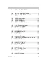
Page 11: ...1 1 Major features 1 1 1 2 System Configuration 1 5 1 2 1 Organization of Slots 1 6 1 3 System Specification 1 7 1 3 1 System Capacity 1 7 1 3 2 Eelectrical Standard 1 9 1 3 3 Power Specifications 1 12 1 3 4 Ring and Tone 1 13 1 3 5 Available Terminals 1 14 1 3 6 Equipment Specifications 1 14 CHAPTER 2 Circuit Overview 2 1 2 1 System Structure 2 1 2 1 1 Block Diagram 2 1 2 1 2 Features of the Comm...

Page 12: ... Board 2 44 2 5 14 4SWM 2 47 2 5 15 WBS24 BTS 2 51 2 5 16 MODEM Board 2 55 2 6 Terminal 2 57 2 6 1 DPIM 2 57 CHAPTER 3 Troubleshooting 3 1 3 1 Diagnosing System Operation 3 1 3 1 1 Checking Cabinet Power 3 1 3 1 2 Abnormal Battery Backup 1 3 3 3 1 3 Abnormal Battery Backup 2 3 4 3 1 4 Checking MP10 11 Board Operation 3 5 3 1 5 Calls are not Connected Highway 3 6 3 1 6 Calls are not Connected Switc...

Page 13: ... 3 5 2 MFM Board 3 56 3 5 3 RCM Board 3 59 CHAPTER 4 Programming for Maintenance 4 1 4 1 Smart Media Programming 4 1 4 1 1 Installation 4 1 4 1 2 Performing Functions 4 3 4 2 CPLD Programming 4 8 4 2 1 Lattice CPLD Programming 4 8 4 2 2 Altera EPLD Programming 4 17 4 3 Offline Programming 4 20 4 3 1 Preparation 4 20 4 3 2 Environment Configuration 4 20 4 3 3 Entering the Offline Test Mode 4 21 CHA...

Page 14: ... 6 1 MP10 Board 6 2 6 2 MP11 Board 6 10 6 3 4SWM Module 6 18 6 4 4TRM Module 6 22 6 5 4SLM Module 6 26 6 6 4DLM Module 6 30 6 7 2BRM Module 6 32 6 8 8TRK Board 6 35 6 9 TEPRI2 Board 6 37 6 10 8COMBO Board 6 43 6 11 16DLI2 Board 6 49 6 12 MGI64 Board 6 52 6 13 MGI16 Board 6 58 6 14 PLIM Board 6 63 6 15 PLIMD Board 6 68 6 16 MODEM Board 6 70 6 17 16DLI Board 6 72 CHAPTER 7 Device Parts Diagram 7 1 A...

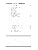
Page 15: ... diagram of the 4SLM Module 2 24 Figure 2 14 Block Diagram of the 16SLI2 16MWSLI Boards 2 27 Figure 2 15 8HYB 8COMBO DLI Block Diagram 2 29 Figure 2 16 8HYB 8COMBO SLI Block Diagram 2 30 Figure 2 17 4DLM Block Diagram 2 31 Figure 2 18 QDASL Block Diagram 2 32 Figure 2 19 QDMC Block Diagram 2 33 Figure 2 20 Block Diagram of the 8DLI Board 2 34 Figure 2 21 Default Configuration Diagram Between the D...

Page 16: ...ramming Mode and the JEDEC File Path 4 13 Figure 4 15 Program Execution 4 14 Figure 4 16 Programming for the MP10 11 Option Board 4 15 Figure 4 17 Changing Information of Part1 4 16 Figure 4 18 Viewing the Chain File When One Option Board Is Mounted 4 16 Figure 4 19 Initial Window of the Altera MAX plus II Program 4 17 Figure 4 20 Program File Selection 4 18 Figure 4 21 Selection of the Data File ...

Page 17: ...Table 1 13 Electric Characteristics of LAN Interface 100 Base Tx 1 11 Table 1 14 Specification of the Power Supply Board 1 12 Table 1 15 System Ring Cycle 1 13 Table 1 16 System Tone Cycle 1 13 Table 1 17 Terminals Compatible with the OfficeServ 7100 1 14 Table 2 1 Types of the Universal Board 2 9 Table 2 2 System Configuration Inter Working With WBS24 2 53 Table 4 1 CPLD List 4 12 Table 4 2 EPLD ...

Page 18: ...Error Use the Home tab to apply 제목 7 제목 7_목차 to the text that you want to appear here XVI SAMSUNG Electronics Co Ltd This page is intentionally left blank ...

Page 19: ... an integrated communications device that can be used as a phone system or PABX Flexible Line Organization The OfficeServ 7100supports an UNI Card The UNI card enables to flexibly organize analog trunk general phone scriber card ISDN BRI Digital Keyset subscriber card etc up to 12 lines depending on user s environment Integrated Communication Environment The OfficeServ 7100 provides data transfer ...

Page 20: ...integrates or resends voice messages and e mails for user s convenience Q Sig Network Function Support The OfficeServ 7100 supports the Q Sig networking function that enables Call Transfer Do Not Disturb DND Call Completion to Busy Subscriber CCBS Call Completion on No Reply CCNR between the OfficeServ 7100 systems or with the iDCS 500 system regardless of the physical location where the system is...

Page 21: ...on The OfficeServ 7100 system is designed in modularity that enables to add hardware such as boards and cabinets and software easily The universal slot of its cabinet allows mounting C O boards extension boards ISDN boards and other special service boards The system programming can be performed via terminals or personal computers connected to the system and it is convenient to change the system co...

Page 22: ...functions more conveniently y Program PC is the PC to maintain and repair the OfficeServ 7100 Users can retrieve change and control various system information by using the program menu on the program PC y Web Management Program The Web management program enables to maintain the OfficeServ 7100 system by using the management program conveniently Users can retrieve change and control various system ...

Page 23: ...riber parts Figure 1 1 Configuration of the OfficeServ 7100 Cabinet Table 1 1 Rear Panel of the OfficeServ 7100 Cabinet Rear Panel of the Cabinet Functions Power Switch Turns the power of the OfficeServ 7100 on off Power I O connector Connects the power cable AC LED Shows the input of the AC power DC LED Shows the output of the DC power Battery Socket Connects external battery Ground Lug Is used f...

Page 24: ...of the OfficeServ Table 1 2 Boards Mountable to Slots Cabinet Slot Mountable Boards Control Part Slot 0 MP10 MP11 Subscriber Part UNI Slot 1 Slot 2 OS 7100 Card UNI board OS 7100 Card 8 16DLI 8 16SLI 2 8HYB 8COMBO 8TRK TEPRI 4BRI LIM MGI 8TRK2 16TRK OS7400 Card TEPRI2 MGI64 Blank Board Function The Blank board is a dummy board that functions as a partition wall to prevent prevents foreign substanc...

Page 25: ...Capacity System Organization Maximum Allowable Lines Cabinet Digital C O line Channels 60 Analog C O line Channels 24 Extension Line Ports 24 VoIP Channels 72 8 MP10 11 64 MGI64 H 323 C O Channels 32 SIP C O Channels 32 SPnet C O Channels 64 Samsung IP Phone Channels 64 WIP Phone Channels 64 SIP Phone Channels 43 ISDN Terminal Channels 32 Voice Mail Channels 4 DTMF Generation Channels 8 CID Creati...

Page 26: ...60 T1 48 E1 60 Extension Line Subscriber Capacity The following table shows the maximum capacity to install general phones and digital phones based on the configuration of the OfficeServ 7100 Table 1 5 Extension Line Capacity System Organization Regular Phone Digital Phone Cabinet 24 24 Number of Channels The following table shows the number in each slot the CID receiver and DTMF receiver of the O...

Page 27: ...O circuit or standard 2500 type set loop Figure 1 2 Loop Start C O line Signaling T1 C O line Signaling The electric characteristics of Ti C O line observes ITU G 703 and G 704 standards Table 1 7 Electric Characteristics of T1 C O line Category Description Transfer Rate 1544 kbit s 50 ppm Code Alternative Marking Inversion AMI or B8ZS Pulse Type The mask feature satisfies ITU G 703 Signal Standar...

Page 28: ...a Twisted pair line Load Resistance 120 Ω Display Pulse Nominal Peak Voltage 3 00 V Blank No Pulse Peak Voltage 0 0 300 V ISDN Interface Transfer Signaling The electric characteristics of ISDN BRI interface observes ITU I 430 and ETS 300 012 standards Table 1 9 Electric Characteristics of BRI C O line Category Description Transfer Rate 192 kbit s 100 ppm Code AMI Pulse Type Mask characteristics sa...

Page 29: ...e listed in the table below Table 1 12 Electric Characteristics of LAN Interface 10 Base T Category Description Transfer Rate 10 Mbit s 50 ppm Transfer Code Manchester encoding Access Control Method CSMA CD Transfer Media UTP CAT3 CAT4 CAT5 STP Number of UTP Pairs Two Pairs Characteristic Resistance 100 Ω Cable Thickness Diameter 0 51 mm 24 AWG External Diameter 5 mm In 100 Base T the LAN signalin...

Page 30: ...the connection between LIM modules Dial Pulse Extension Line Signaling y Rate 10PPS Pulse Per Second y Make Break M B Ratio 33 66 adjustable based on software y Minimum time between digits 20 msec adjustable based on software DTMF Push Button Dialing Extension Signaling The DTMF signal processing follows the ITU standard for the transmission and reception on the C O line side of digital phone sign...

Page 31: ...hanging the system database value Tone The ring signal output voltage and frequency of the OfficeServ 7100 are as follows y Output Voltage 75 V y Frequency 20 Hz The OfficeServ 7100 provides some tones to guide users the progress status of the functional operation and provides the feedback for the status The On Off cycle for each tone specified are as follows Table 1 16 System Tone Cycle Tone ON O...

Page 32: ...00 Series DS 24E DS 24D Series DS 2024E DS 2024E DS 2021E DS 3020 Series AOM DS 5064BAOM DS 4014AOM DS 4064AOM DS 24SE AOM DS 2024EAOM DS 3020SAOM The 16DLI boards of OfficeServ 7100 system can interwork up to 16 AOM terminals and the 8HYB boards can interwork up to 8 AOM terminals Others KDB S KDB D DPIM door phone Compatible Terminals OfficeServ 7100 can use all compatible terminals of the iDCS ...

Page 33: ...OfficeServ 7100 Service Manual SAMSUNG Electronics Co Ltd 1 15 ...

Page 34: ...CHAPTER 1 Error Use the Home tab to apply 제목 1 장 제목 1 to the text that you want to appear here 1 16 SAMSUNG Electronics Co Ltd ...

Page 35: ...tem 2 1 System Structure This section describes the physical structure and the communication structure between the cabinets of the OfficeServ 7100 system 2 1 1 Block Diagram The physical structure of the OfficeServ 7100 system is as shown in the figure below Figure 2 1 Physical Structure of the OfficeServ 7100 System Power 5 V 5 V 12 V 3 3 V 54V54 V Mother Board SLOT1 SLOT2 MISC LAN SIO MP10 11P10...

Page 36: ...it serial bus type y Since the OfficeServ 7100 uses the standard multimedia interface it can be upgraded by using the large scale multimedia card that can be easily purchased on the market y The multimedia of the OfficeServ 7100 system uses the power of 3 3 V y The multimedia card can be mounted on the front panel of the MP 10 11 board Caution for the use of Multimedia Cards Only the Multimedia ca...

Page 37: ...U SRAM and SDRAM of the MP10 11 board are connected by using a 320 bit bus y One system SIO is provides on the MP10 11 board Ethernet Access y In default Ethernet access is provided SIO Port Usage y One debugger port is provided to assist a system engineer to inspect the system status ...

Page 38: ...2 3 Power Supply Module The power supply module supplies power to the cabinet of the OfficeServ 7100 This module operates by AC input power or battery power and supplies the powers of 54 V 5 V 3 3 V 5 V and 12 V to the cabinet If the system operates with the AC power the module supplies 0 4 A for battery charge when there is no remaining current due to battery discharge 2 4 Control Board The contr...

Page 39: ...32 Address Date Internet HW4 HW 0 3 HW5 SRAM K6F8016U6 VCXO 16 Mhz RTC 72423 ENGINE STC9604 CPLD LC4256V PLL EEPROM AT03C46 Clock 10 Mhz SDRAM K4S561632 PHY ADM7001 X 2 MMC DRIVER TE4300 UARTO RMII GPIO 8 23 EXP_BUS GPIO 0 7 UART1 Voice Mail 4 Channel SPI REF_CLK SDR_BUS Main Processor VOIP 8Channel BACKUP CC T P1 P2 P3 P4 MOTHER R D Boot Rom SST39VF040 Buffer Daughter B d 4DLM 4SWM MC MD1 LAN LED...

Page 40: ...r for VoIP packet processing y uP Bus interface or PCI interface support y Additional SDRAM interface y NAND Flash Device specifications y Various OS support System Clock The MP10 uses 10 MHz as the main clock oscillator This clock creates 375 MHz inside the CPU Boot ROM Flash ROM A flash ROM of 512 KBytes is used as the Boot ROM The Boot ROM downloads the system main program required for the syst...

Page 41: ...de it does not need the change of the hardware even if the capacity is increased The card should be always installed to the system for its operation The card should be wrapped in vinyl used in the purchase of the card for the preservation Internal Music One channel is provided for the internal sound source of the system CODEC supports both A LAW method and U LAW method and the relevant CODEC is op...

Page 42: ...peed is 100 Mbps Once the system is connected to LAN the speed is detected automatically and LAN is operated Universal Asynchronous Receiver Transmitter UART The UART is an element that enables asynchronized serial communication and is used as the system I O port SMDR or PCMMC The UART connects to outside via the RJ 45 connector in front of the cabinet and the speed is 115 2 kbps EEPROM The EEPROM...

Page 43: ...e 2 1 Types of the Universal Board Board Type Board Name C O line Board 4TRM UNI 2BRM UNI 8TRK TEPRIa TEPRI2 Extension Line Board 4DLM UNI 4SLM UNI 8SLI 16SLI2 8DLI 16DLI2 8Combo Service Board MGI16 MGI32 Data Service Board 4SWM MP10 LIM P LIM P2 2 5 1 UNI Board The UNI board supports the newly developed daughter boards of the OfficeServ as the interface board types mounted on the OfficeServ 7100 ...

Page 44: ... Diagram Figure 2 4 UNI Board Block Diagram P2 P1 P4 P3 MD3 P2 P1 P4 P3 MD2 P2 P1 P4 P3 MD1 MD2 MD1 MD3 LED FRONT PANEL Primary Connector Secondary Connector Module 3 Primary Connector Secondary Connector Module 2 Primary Connector Secondary Connector Module 2 FGND MOTHER B D Other Signal ADDRESS DATA CPLD POWER CONTROL 54 V BUFFER P1 P2 P3 ...

Page 45: ...rd y parts 3 177986 4 100 Pins SMD type 1ea Frame GND Support This is a support to supply FGND to each daughter board and has the same height as those of the primary and secondary connectors External Network Interworking Part The above primary connector part uses a RJ 45 12 Port Modular Jack Connector to directly connect an outside network Four ports are allocated to each daughter board module y P...

Page 46: ...o three 4TRM modules can be mounted on an UNI board and the OfficeServ 7100 system can mount the maximum 6 6TRM modules 2 5 2 1 Block Diagram The following figure shows the 4TRM block diagram The circuit in the blue box is the 4TRM module and the block diagram describes the connection to the UNI board Figure 2 5 Block Diagram of the 4TRM Board DAA Hook SW RING DET PRS CID CO1 DAA Hook SW RING DET ...

Page 47: ... Off On y CID Detection y PRS detection y Loop Supervision y DC AC termination y Primary secondary separation and Line Balancing The following figure shows the DAA chip block diagram Figure 2 6 Block Diagram of the DAA Chip Transmit Isolation Amplifier Receive Isolation Amplifier Snoop Amplifier Ringing Detect Outputs Half Wave Fault Wave RING RING2 Rx Rx OH MODE Tx Tx Isolation Barrier Csnoop Csn...

Page 48: ...tics 4W Return Loss adjustment y CODE DECODE y Time Slot Assignment function The following figure shows the QSLAC block diagram Figure 2 7 Block Diagram of the QSLAC Part Time Slot Assigner TSA Clock Reference Circuits Signal Processing Channel 1 CH 1 VIN1 VOUT1 Signal Processing Channel 2 CH 2 VIN2 VOUT2 Signal Processing Channel 3 CH 3 VIN3 VOUT3 Signal Processing Channel 4 CH 4 VIN4 VOUT4 SLIC ...

Page 49: ...ther keyphone system The module carries out the Real driver Ring detection TSAC and CODEC control functions by TMC ASIC 2 5 3 1 Block Diagram The following figure shows the 8TRK board block diagram Figure 2 8 Block Diagram of the 8TRK Board ASIC STL7053 CODEC Part Address Control DATA MBD Interface HYB Matching Line 1 Interface CODEC Part Line 4 Interface HYB Matching ASIC STL7053 CODEC Part HYB M...

Page 50: ...ign circuit The Hybrid circuit for impedance matching is designed as the Hybrid circuit for the line impedance of 600Ω Voice Sending Receiving Part This part performs the surge protection function via the primary protection to withstand the high voltage supplied between tip lead and ring lead In addition the part constructs the tertiary protection circuit by using a zener diode inside the impedanc...

Page 51: ... signal is transmitted in the different path from the transmission path Ring Reception Detection Circuit The ring reception signal transmitted from the C O switch is transmitted as the incoming signal when the C O interface is in Hook on mode The DC voltage of the ring signal is cut off by the Poly capacitor of 0 47 uF 250 V on the normal contact of the loop relay After that only the ring signal o...

Page 52: ...erface board to provide the BRI board with two ports This module is connected to 4 channel ISDN trunk in S mode or T mode 2 5 4 1 Bk Diagram The following figure shows the 2BRM block diagram Figure 2 10 Block Diagram of the 2BRM Board S T Interface chip PEB3086 S T Interface chip PEB3086 TRANS APT 2S0 22A TRANS APT 2S0 22A 16 pin connector UNI b d 100 pin connector UNI b d OSC 7 680 Mhz BRI 1 S T ...

Page 53: ...on between S T interface and ISDN Oriented Modular IOM y Receive timing recovery according to a specific operation mode y D channel access y Activation and deactivation procedures automatic wake up in power down state Layout between 2BRM and UNI The 2BRM is a daughter board mounted on the UNI board and interfaces with the primary side 16 pin connector and the secondary side 100 pin connector The I...

Page 54: ... Slot 1 2 4 11 in the cabinet supporting 64 channel among from the universal slots of each cabinet 2 5 5 1 Block Diagram The following figure shows the TEPRI2 board block diagram Figure 2 12 Block Diagram of the TEPRI2 Board SIO Interface MAX3232E ENGINE STL7065 CPU MPC852T RST FALC 56 PEF2256H FALC 56 PEF2256H APPLI FROM AM29LV320 SDRAM K4S641632H BOOT FROM SST39VF040 LED Indicator Line Interface...

Page 55: ...d Signaling CAS via Common Channel Signaling CCS CPU MPC852T This is the main processor and MPC852TZT50 by Motorola Inc is used for this The the data bus of this CPU is used in 32 bit mode The main specifications of MPC852T are as follows y Embedded Power PC core y 4 Kbyte Data cache and 4 Kbyte Instruction cache y Memory Management Unit MMU y 32 bit Dynamic Bus Controller y 32 bit Address Lines y...

Page 56: ...tion ROM Flash ROM y Application ROM uses 4 Mbytes flash ROM AM29LV320D y Application ROM is used as and stores application programs SDRAM y SDRAM uses 16 Mbytes DRAM K4S641632 and consists of two 8 Mbytes elements y The main program resides in the SDRAM and the SDRAM stores the data for the system processing The RAM backup is not required y The access time to SDRAM is set as short as possible for...

Page 57: ... 3 Wire Serial 1kbit EEPROM AT93C46 128 byte y The unique hardware number of a board is assigned in initial factory manufacture y The EEPROM is connected to the Serial Peripheral Interface SPI in CPU for the communication Reset y The reset chip uses DS1706RESA y The types of the reset are power on reset push button reset software reset Watch Dog reset etc CPLD y The CPLD establishes the most logic...

Page 58: ... 5 6 2 Major Features Module Interface Part The UNI module interface of the 4SLM board is roughly divided into Power PCM and SPI y Power 3 3 V 5 V and 54 V are supplied in the UNI board y 3 3 V Supply the power for Le88241 Operation and operates LCX125 a Highway buffer y 5 V Input power of the switching regulator in Le88241 y 54 V Is converted into 12 V power via LT1170 Switching Regulator The 12 ...

Page 59: ...ia the UNI boards by using the SPI bus The most operations and functions of the 4SLM board are determined by Le88241 The major features of Le88241 as follows y Sine Wave Ringing Generation y DC Feeding y Loop supervision detection y 2 4 wire balance y Transmit receive gain control y A law u law selection The Le88241 consists of the following blocks y Digital Interface Block This is the interface b...

Page 60: ...e software control y Switching Regulator Controllers This circuit is added to the Le88241 to create high voltage such as Feeding voltage and Ringing signal required for the operation of the SLT Interface The switching regulator is controlled by the Le88241 in term of software In short feeding current voltage and ringing signal voltage frequency are controlled by the SPI command 2 5 7 16SLI2 16MWSL...

Page 61: ...Relay MW Relay SLIC DC FEED HOS PWM SLIC DC FEED HOS PWM SLIC DC FEED HOS PWM SLAC CODEC GAIN Control SERIAL I F for REGISTERs in SLAC EPLD CARD ID PROTECTION CCT RELAY CCT X 4EA EPLD DRIVER CCT CLOCK CCT 4 096 MHz 2 048 MHz FOI FS RINGER 20 25 HZ 48 V MOTHER B D 5 V MOTHER B D 3 3 V MOTHER B D MESSAGE VOLTAGE RINGER CCT RINGER Selection SW EXT RINGER CCT SINE WAVE Frequency Divider PWM FREQ HOS D...

Page 62: ...ernal ringer circuit to use the MW voltage even if it uses an external ringer The period of the MW lamp can be controlled in KMMC 511 The continuous LED always turns the lamp on To turn on off the lamp periodically proceed the following procedure 1 Select Interrupt LED and press the Right soft button 2 By using the Right soft button move to the time period 3 Enter the ring period data in the seque...

Page 63: ... and 8DLI functions and mounted on the universal slot of OfficeServ 7100 2 5 8 1 Block Diagram DLI DLI block diagram of 8HYB 8COMBO board is as follows Figure 2 15 8HYB 8COMBO DLI Block Diagram Line 1 Interface Line 2 Interface Line 3 Interface Line 4 Interface QDASL TP3404 Line 5 Interface Line 6 Interface Line 7 Interface Line 8 Interface QDASL TP3404 ASIC STS9511 Address Control DATA 30 Pin x 2...

Page 64: ...ction y Tone generation y 8 analog extension ports 8 digital extension ports y The SLI function of 8 ports and the DLI function with 8 ports in one board y By using 8 RJ 45 ports 16 ports are configured The internal 4 5 pins are used as the SLI port and the 7 8 pins are used as the DLI port RJ 45 x 8 TIP Ring Signal PFT relay Relay x 8 Transformer x 8 RING Generator Balance Hybrid x 2 CODEC IC TP3...

Page 65: ...rv 7100 4DLM performs the same operation as that of 16DLI2 and includes four ports 2 5 9 1 Block Diagram Figure 2 17 4DLM Block Diagram QDASL TP3404 V QDASL controller STI 9511 DLT 1 Port 1 LI1 LO0 DLT 1 Port 2 LI1 LO1 DLT 1 Port 3 LI1 LO2 DLT 1 Port 4 LI1 LO3 D0 C0 DI CI INT CS CCLK SA 1 7 WR RST CS INTS INTD SD 8 15 100 pin connector MP10 UNI b d 54 V 16 pin connector MP10 UNI b d FSX CLX 4M_CLK...

Page 66: ...ta to QDMC Then QDMC converts the serial data to parallel data through UART and transmits the data to CPU y Quad 2B 1D channel interface y 144 kbps full duplex in one twisted part y Loop range 6kft 24AWG y Alternate Mark Inversion coding transmit pulse shaping DAC Smoothing Filter scrambler for low EMI radiation y Programmable Time slot Assignment TDM interface for B channels Figure 2 18 QDASL Blo...

Page 67: ...Marking Inversion AMI in a full duplex method of 144 kbps is used Voice and data channels are available for end to end communications The actual transmittance rate from the 8DLI board to the digital phone is 192 kbps 16 kbps from 48 kbps where 144 kbps of 2B D above is excluded is used for synchronization and remaining 32 kbps is used for transferring null data Lines of AWG 26 thick are used as tr...

Page 68: ...n expanded form of the existing TP3401 3402 3403 This chip is made in the following procedures The transceiver in a single channel Time Compression Multiplexed TCM transmission method is expanded to 4 ports and micro wired control and other control structures are changed The functional features of the QDMC are as follows y Transfers receives data in a UART format for D channels y A UART speed 2 4 ...

Page 69: ...time slot which is D channel where 256 channels of 2 bit are allocated The sub time slot means that the B channel of 8 bit is divided into four To receive D channel data of 1 byte from the QDASL the data of 4 frames should be received first QDMC provides 128 sub time slots Digital Phone Interface The AMI code is created from the QDASL TP3404 and is transmitted to regular phones through the Trans T...

Page 70: ...ed in the line and the Zener diode prevents against external high voltage Figure 2 21 Default Configuration Diagram Between the Digital Phone and System Figure 2 22 Data Transfer Format Diagram M C U DIGITAL TELEPHONE SLAVE x 8 DMC DLI card CODEC Transmission I C DASL Transmission I C DASL PCM HIGHWAY SYSTEM MASTER 2B D 2 Wire TIME SWITCH CPU B1 BITS B2 BITS D 2b B1 BITS B2 BITS D 2b SLAVE BURST M...

Page 71: ...k are used as transmittance lines between the 16DLI board and digital phone and maximum transmittance distance is 400 m The DLI board supplies the power of 48 V to the phone and is configured with the poly switch that disconnects over current and circuits for digital interfaces This board controls 48 V of power on or off through the FET inside of the 8DLI board The UART inside of QDMC has three Rx...

Page 72: ...23 Block Diagram of the 16DLI Board QDMC STI9511 Address Control DATA MBD Interface QDMC STI9511 Line 1 Interface Line 2 Interface Line 3 Interface Line 4 Interface QDASL TP3404 Line 5 Interface Line 6 Interface Line 7 Interface Line 8 Interface QDASL TP3404 Line 9 Interface Line 10 Interface Line 11 Interface Line 12 Interface QDASL TP3404 Line 13 Interface Line 14 Interface Line 15 Interface Lin...

Page 73: ... for serial data transfer AMI codes created along with B channels are transmitted to the line and the D channel data are used for controlling phones The B channel data are used for generating voice signals INTD processes the micro channel interrupt of QDASL in each port The INT of the QDASL is generated only when accessing the micro channel and initializing the QDASL The INT is generated in the ev...

Page 74: ...the entered serial data to parallel data through the UART and transfers the data to the CPU Also TSB of the QDASL transfers the voice data of DASL to the highway Since one QDMC controls two QDASLs a total of 8 ports the TSB signals generated from each QDASL are added for use DLT 1 is used for a Trans for matching and resistance of 100Ω in the QDASL LO adjusts impedance 2μF reduces noises Two Zener...

Page 75: ...MGI64 MGI16 board is shown in the figure below Figure 2 24 Block Diagram of MGI64 MGI16 board PCM Interface part 2 048 MHz x 2 MBD MBD DATA BUS Flash 8 MB 16 bit TE28F640 J3C120 SDRAM 64 MB 32 bit K4S561632E TC60 x 2 CPU DSP M82530L 14 MGI16 ÆM82511 125 MHz FPBGA 484PIN Voice FAX Compressing part G 723 G 729 MAIN Interface part DPRAM 512 b x 2 IDT71321LA35PF Flash 512 KB 8 Bit SST39VF040 x 2 Reset...

Page 76: ...bps on the average through silence suppression y TIA 464A DTMF detection generation y MF detection generation y Parallel hist processor interface y Tone signal that the host can program y PCM interface that can be configured PCM highway or parallel interface y On chip PCM highway interface host configuration time slot allocation and selectable G 711 μ law A law PCM interface y Gain control RS 232C...

Page 77: ... certain time after reset signals are generated until the power is stable after the power is turned on and properly operates y WATCH DOG Timer Reset Through the OSC internal clock transmitted to CPLD if CPU does not access a specific address in CPLD within 5 seconds board reset is generated y Manual Reset Detects the reset switch being pressed Reset switch connects the reset signal in CPLD through...

Page 78: ...ck Diagram The block diagram of the PLIM board is shown in the figure below Figure 2 25 Block Diagram of the PLIM Board SWITCH VT6526CF VIA 24 Port FE_PHY VT6108S VIA 8 Port FE_PHY VT6108S VIA 8 Port FE_PHY LXT972LC Intel S3MII x 8 S3MII x 8 MII MAGNETIC H1164 PULSE 4 Port MAGNETIC H1102 PULSE PSE PD64004 4 Port Daughter Board PLIMD Back Board I F WIM 16 bit Local Bus PSE PD64004 4 Port PSE PD6400...

Page 79: ...e and Intelligent CPU mode The Bootstrap mode sets a physical mode depending on whether specific pins of the chipset are set to high or low at initial boot in non management switch mode The EEPROM mode sets chipset configuration by getting register settings from the NM24C08 connected to the VT6526 at initial boot The Intelligent CPU mode is used when inter working with the WIM board This mode obta...

Page 80: ...ction Thus remove the PoE power source selection pin J1 J2 J3 in PLIM board Figure 2 26 PoE Strap Option of PLIM Board Shunt Removal in PLIM If PLIM card is mounted on OfficeServ 7100 system the PoE function is not supported Thus when PLIM is mounted on OfficeServ 7100 system check if the shun pin for selecting the PoE power is removed from the connector J1 J2 J3 J1 1 J2 J3 1 1 ...

Page 81: ...sor LAN port Four LAN ports of the front panel provide the 802 3af PoE function by default 2 5 14 1 Board Connection Configuration Diagram The configuration diagram of connecting 4SWM to MP10 board or MP11 board is as follows Figure 2 27 4SWM Configuration Diagram Reserved Pin in case of M82511 Not assembly in case of MP10 M82810 M82511 RMII RMII Tx RX Pair Tx Pair Rx Pair VCC BCM5325 4SW Module M...

Page 82: ...ddition it provides one 10 100 MII interface and can be configured as the sixth port and connected to Reversed MII of the processor In 4SWM it is used as the sixth port If 4SWM is mounted it switches with LAN of MP10 11 Packet buffer memory and one address resolution engine are mounted and non blocking switch controller and Management Information Base MIB statistics register are also included 4SWM...

Page 83: ...3 3 1 8 V 0 18 um CMOS technology y HP auto_MDIX function hardware selectable y 128 pin MQFP package y Ingress egress rate control y Protected port capability y DTE DPM power over Ethernet detection CPU Interface For BCM5325E of 4SWM the management function is controlled by Mindspeed Processor in MP10 11 The communication between BCM5325 and the processor is established through the Synchronous Ser...

Page 84: ...vided as BCM5241 in BCM5325 Through MDIO the registers of BCM5241 are transmitted In the processor if Register Page 0x18 MII Port External PHY Register of BCM5325E is controlled BCM5325E access BCM5241 automatically through MDC MDIO pin Power Over Ethernet Control Block Power over Ethernet PoE supplies 48 V to the device of the counterpart through the LAN cable of RJ 45 This can be classified into...

Page 85: ...US 16bits DASL_Int PCM I F 20MHzXtal Voltage Regulator Input 5V Output 3 3V 1 8 V 2 048MHz OSC K PI F 54V RJ 45 PowerJack RJ 45 DC DCPower Remote 54V 5V 3 3V Magnetic Reset External Antenna Diversity Gain 2dBi Dipole WLAN NIC CARD 802 11b MAC BB Ext Ant Reset Control PCMCIA Power Controller 3 3V 5V Auto Switch SRAM 64 K word JTAG Connector CPLD 10pin CPU DSP 14pin Serial Boot ROM 512kbyte SDRAM 16...

Page 86: ... one 4WLI board is installed into the OfficeServ 7100 system y One 4WLI board can inter work with up to four WBS24 BTSs y Calls can be made simultaneously through up to four voice channels per WBS24 BTS y A frequency can reach to 50 m indoor the distance depends on communication jamming objects at the office and 200 m outdoor when communication jamming is not made within the sight distance y This ...

Page 87: ...as two types of interfaces wire and wireless The wire interface is classified into the interface that inter works with the system and the interface that inter works with the LAN The wireless interface inter works with air section and meets the IEEE802 11b standard Wire Interface Inter Working With the System This interface is connected with 4WLI by Digital Adapter Subscriber Loops DASL which enabl...

Page 88: ...ntersil Co Ltd and external antennas can be installed into the board If the voice or data packets forwarded or received in a wireless are occupied in the air section in a CSMA CA method first other BTSs will have opportunities of forwarding or receiving once the first BTS completes forwarding or receiving Thus multiple terminals can forward or receive packets in a wireless section Since multiple t...

Page 89: ...ected to OfficeServ 7100 system through V 24 interface and uses the modem chip for central office that PCM highway interface is available In addition the modem board supports the V 90 protocol Modem board is controlled through the serial communication type in OfficeServ 7100 and the command used is standard AT command SMC2 is allocated and used as the serial port for modem control 2 5 16 1 Block D...

Page 90: ...ics Co Ltd 2 5 16 2 Main Features This section describes the main features of the modem board PCM Interface For the channel for modem channel 0 is allocated to highway 0 The PCM interface is as follows Figure 2 32 PCM Interface of Modem Board FOI FOX CLKX HWR MSB D6 D5 D4 D3 D2 D1 D0 MSB D6 D5 D4 D3 D2 D1 D0 Hi Z HWX ...

Page 91: ...reviously developed and is currently being used by connecting it to the OfficeServ 7100 system The longest available distance between the DPIM and the OfficeServ 7100 is 400 m and the calling distance between the DPIM and the door phone is 200 m The longest calling distance from the main door phone is 600 m 2 6 1 1 Block Diagram of DPIM The block diagram of the DPIM is described below The DPIM use...

Page 92: ... part T5692 is used along with the trans of the door box The resistance of 1 kΩ R14 is the resistance value when two trans have the best quality of transfer Also since the resistance of 100 kΩ R9 R10 uses the signals transmitted and received from to the trans by mixing them it is a balance resistance for decreasing the input of the signals which are transmitted to the speaker to the micro input of...

Page 93: ...trans is not damaged 12 V Generating Part The DPIM uses the step up DC converter LT1109 U11 that generates 12 V in the simple surrounding circuit by the 5 V power being entered LT1109 12 displays 12 V 60 mA by the input of 5 V The 33 uH L2 inductor is for generating the switching and the 47 uF 35 V C7 capacitor is for the load of the switch and the 33 uH L1 inductor of the output end is for decrea...

Page 94: ...CHAPTER 12 Error Use the Home tab to apply 제목 1 장 제목 1 to the text that you want to appear here 2 60 SAMSUNG Electronics Co Ltd This page is intentionally left blank ...

Page 95: ...ccur while operating the OfficeServ 7100 system and their troubleshooting 3 1 Diagnosing System Operation Describes problems that may occur while operating the system and their troubleshooting 3 1 1 Checking Cabinet Power The procedure for checking if the power of Power Supply Unit PSU of cabinet is properly supplied is as follows ...

Page 96: ...58 V measured No No Yes Yes Yes Turn on the cabinet power switch Is only AC LED on No Check the battery fuse F3 F4 of Power Supply Unit Left fan operates properly Yes No No Check the AC fuse F1 F2 of Power Supply Unit PSU Check the voltage in J1 of main mother board 54 V PIN8 PIN9 5 V PIN3 6 PIN7 5 V PIN3 6 PIN1 12 V PIN3 6 PIN2 3 3 V PIN3 6 PIN4 5 Check if AC DC LED is turned on Check the directi...

Page 97: ...lem of battery backup is not resolved refer to 3 1 4 Abnormal Battery Backup 2 When battery is connected or battery is on off while the AC power is not supplied system does not operate Supply the AC power to charge the battery Check the battery voltage Is the battery voltage over 53 V Is the battery voltage below 47 V Yes Yes No No Check the battery connector Check the battery cable Analyze system...

Page 98: ...tor followed the 3 1 3 Abnormal Battery Backup 1 procedure follow the items below Is the LED of MP10 11 turned on No Yes Connect the battery and turn the battery switch on Check if the PSU connector is connected while the system power cord is pulled off If 54 V is not generated check the battery connection If the battery connection is proper check the fuse of PSU Check the battery voltage while th...

Page 99: ...ows Does the MC LED of the MP10 11 board blink rapidly download After the MC LED blinks does the RUN LED blink again No No Yes Yes Check the multimedia card insertion status Replace the multimedia card After downloading check if the MP10 11 LED blinks properly End Noprmal LED status MP10 11 Blinks MC Turns on LAN Blinks during LAN operation Check the multimedia card program version Turn the power ...

Page 100: ...blem when the operator starts to make a call by connecting a phone to the OfficeServ 7100 system If a specific group of slot 1 2 groups cannot be connected to a call check and replace the slot for 16 ports There is a board where a call can be connected No Yes No Yes If the MP10 11 operation normal No Yes After board is replaced the operation is normal Check the 3 1 5 MP10 11 board Scope the line b...

Page 101: ... starts to make a call by the phone connected to the OfficeServ 7100 system Is the power of digital analog phone turned on Yes Refer to 3 1 1 Checking Cabinet Power Check the ADDR DATA bus of MP10 11 board or main board Start End After the board is replaced the system operation is normal Check the 4M FOI signals of MP10 11 board Yes No No If a specific group of slot 1 2 groups cannot be connected ...

Page 102: ...ckground Music sources BGM is Abnormal The procedure for resolving the problem that occurs when MOH BGM of the OfficeServ 7100 system is abnormal is as follows Is a call connected properly Check the time switch operation Yes Start No Repair the time switch Does the source set to MMC 309 perform properly Check the MMC setting No Yes Replace MP10 11 board ...

Page 103: ...e The procedure for resolving the problem that occurs when external announcement is not available is as follows Is a call connected properly Check the time switch operation Yes Start No Repair the time switch Does the source set to MMC 309 perform properly Check the MMC setting No Yes Replace MP10 11 board ...

Page 104: ...US are abnormal check which path causes the error up to MP10 11 board Yes No Check the 4 MHz and FOI signals sent from MCP board Check the 4 096 MHz CLKX and FSX signals generated from U21 STL9604 Check signals in buffers of MP10 11 board U19 If buffer input is abnormal check from U2 to buffer If buffer output is abnormal replace the buffer Check the 4 096 MHz CLKX and FSX signals generated from U...

Page 105: ...o of ports mounted on board exceeds the power supply board capacity Is the board detected No Yes Replace two transistors driving FET Reaplce FET Replace the power supply board Change the No of ports Check the ADDRESS DATA BUS EN WR signals of the board Is the TIP RING power of DLI or SLI generated below 39 V In DLI board is POWER CONTROL of the corresponding slot ON Check if the corresponding boar...

Page 106: ... signal ACTIVE LOW No Yes Y1 power 4 is abnormal Check adjacent circuits Y1 power is normal but output is abnormal Replace Y1 Track the DTACK source and check the operation such as source clock in HIGH status DTACK of option board DTACK of main board DTACK of the time switch U26 DS1706 if STEADY LOW If CPU ADDR DATA bus if VIBRATION Is at least one LED of MP10 11 board s ON No Refer to 3 1 1 Check...

Page 107: ...urs when internal MOH BGM is abnormal is as follows In this case MOH is set as internal MOH No Yes No Yes Scope if signals are generated from PIN1 of U28 Is it normal No Yes Repair the port failed Replace U27 Replace U28 Start Are signals generated properly from PINs of U27 Is the communication between ports normal Check if the corresponding channel signal of highway TX is generated ...

Page 108: ...noise while calling Is DUTY of FOI signal steady No Yes Is REFERENCE clock selection MMC selected No Yes Is the REFERENCE clock normal No Yes Is 2 kHz norma No Yes Start Check if the corresponding channel signal of highway TX is generated Set the REFERENCE clock Check the REFERENCE clock of TEPRI board main board and MP10 11 board If REFERENCE clock sometimes shakes TEPRI line is abnormal If REFER...

Page 109: ...em caused by system UART port operation of cabinet when MP10 11 board is used is as follows No Yes No Yes Replace U20 Check MMC Check the S W version Check if other functions operate properly Replace CPU U1 Start Check the connection up to RJ 45 Is TXD of U20 MAX3232 generated Is signal generated from E4 UART_TX PIN of MP10 11 CPU ...

Page 110: ... for resolving the problem that occurs when memory and time data of the OfficeServ 710 system is being backed up is as follows Is the programmed memory and time data identical with that of the original value Yes No VDD PIN24 of the clock chip U12 is over 2 V continuously Yes No Connection between S1 SWITCH and D8 is properly established Yes No Replace the corresponding part Start End ...

Page 111: ...ltimedia card is as follows No Yes No Yes Check the program version Check the MP10 11 CPLD version Check MP10 11 ADDR DATA BUS Insert to the multimedia card slot Replace the multimedia card Start Replace the multimedia card After MC LED of MP10 11 board blinks rapidly does MP10 11 LED blink Does MC LED of MP10 11 board blink rapidly during booting ...

Page 112: ...upper side of the cabinet and check the 4SWM module Then there is LED that displays the status Through the LED operation status can be identified y LED ON Link On y Blink Data Communication The procedure for resolving the problem of LAN operation of the 4SWM board is as follows NO Yes No Yes No Start The ping test result is normal Check the trace of each port and the switch port output scoping Che...

Page 113: ...lem of PoE operation of the PLIM board is as follows No Yes No Yes No End Yes Start It operates in a specfic port Replace U4 The power supply of the port connected is normal Check the LAN cable Check Strap Option Check the terminal connected Check the part and pattern between T1 and U4 port U4 port output 1 2 3 4 40 43 45 48 power ...

Page 114: ...ection describes the problems and troubleshooting the problems that occur in UNI board 3 4 2 1 LED does not Operate No All LEDs do not operate Replace the LED of the port No Check the PSU output and replace PSU Yes Replace CPLD U1 Yes Yes End Start Check the CPLD U1 LED output 3 3 V power is normal Check the pattern and resistance between U1 and LED ...

Page 115: ...ace and check Q3 The power output in D1 CATHOD is abnormal 54 V power is not supplied to the entire module Check the signals in U1 and replace U1 The R61 power supply is normal Yes Yes Yes Check the 54 V pattern CTRL_PWR signal is normal Check the PSU output voltage and the UNI card input power M54 pin 3 4 2 2 54 V Power is not Supplied to Module ...

Page 116: ...nics Co Ltd 3 4 2 3 Abnormal UNI Operation After checking the MB output replace MB End No Yes Replace the buffer Start CPLD U1 output is normal CPLD U1 input is normal Buffer U2 U3 input signals are normal Check the signal pattern and take actions Replace U1 Buffer U2 U3 input signals are normal Yes Yes Yes No No No ...

Page 117: ...e 4TRM No Yes Replace the line and check the pattern part up to the port termial Yes Yes No Yes Start Transistor Q101 Emitter is normal Inverter U104 output is normal CPC5623 Pin 10 is normal Pin 13 14 of CPC5623 are normal Ring detection is performed in the entire port End Replace the transistoer Replace the inverter Replace CPC5623 No Yes No No ...

Page 118: ...appear here 3 24 SAMSUNG Electronics Co Ltd 3 4 3 2 Hook On Off is not Available Yes Check the line and U1 End Replace CPC5623 Pin8 iput of CPC5623 is normal Start Replace and check UNI Hook On Off is not performed in all ports U1 input 24 31 32 33 is normal Replace U1 Yes Yes No No No ...

Page 119: ...ircuit of U2 and replace it Check adjacent circuit of Switching Regulator T200 and replace it Check adjacent circuit of Switching Regulator T200 and replace it Start Le88241 Pin 69 input is 90 V Le88241 Pin 1 input is 90 V 12 V power is normal 54 V input power is normal Ring generation is not available in all ports Replace Le88241 End Yes No No No Replace UNI and check PSU ...

Page 120: ...t Detected The procedure for resolving the problem that occurs when 8TRK is not detected is as follows Check the signals of DATA BUS and CARD ENABLE of board Yes No Does a problem occurs when the corresponding 8TRK board is mounted Yes No Are all slots abnormal Yes No Does a group not operate Replace the MP10 11 board Check with normal board again Repair MP10 11 board Check if a group from slot 1 ...

Page 121: ...e board No Yes Yes Check if RELAY control signal is normal No No No Check if the absolute power between TIP RINGs exceeds 30 V in the hook on status Replace C O line loop HYBRID Replace RELAY Repair the C O line Replace TMC LINE1 4 U5 LINE 5 8 U6 Replace TMC LINE1 4 U5 LINE 5 8 U6 Is the power normal When the C O line is occupied check if RELAY operates by sound RELAY operation is normal HOS is HI...

Page 122: ...for resolving the problem that occurs when C O line ring is not terminated is as follows No Yes No Yes Repair the C O line Check if the ower provided to TIP RING exceeds 40 VRMS Raplce TMC LINE1 4 U5 LINE 5 8 U6 Is the HOS output HIGH Does the power provided to ring exceed 40 VRMS Check the ring path composed of R C and two ZENER diods Replace LOOP HYBRID and PHOTO COUPLER ...

Page 123: ...onnector Yes No Check the signals of HWX PIN11 of CODEC and BCLKX PIN9 10 of CODEC No Is the RX signal detected Check the PIN 14 of the CODEC Yes Check the abnormal part by tracking up to C O connector Yes No Is PIN3 TX abnormal Check TX and RX signals on PIN3 and PIN14 of corresponding CODEC Yes Check PIN9 10 BCLKX PIN5 12 FS PIN6 HWR and PIN11 HWX of CODEC Yes Yes Is PIN14 RX abnormal Check PIN9...

Page 124: ...procedure for resolving the problem occurs when TEPRI2 is not detected is as follows Check the signals of DATA BUS U16 CARD ENABLE U16 and ADDRESS U17 signals Yes No Problem occurs when the TEPRI2 board is mounted Check if all boards do not operate Yes No All boards do not operate Yes No A group does not operate Repair MP10 11 board Check with normal board again Repair MP10 MP11 board Repair the b...

Page 125: ... abnormal Reaplce Y1 Refer to 3 1 1 Checking Basic Cabinet Power Check 30PIN connector status If PIN602 of DPRAM U14 is STEADY LOW replace U14 or upgrade to final program Repair BUS SHORT OPEN PORT FAIL Replace Y2 Replace with U3 DS1706 or U5 CPLD if STEADY LOW Check CPU ADDR DATA BUS if VIBRATION Start End Check ADDRESS DATA BUS Y2 signal is normal BUS is normal DTACK signal is ACTIVE LOW RESET s...

Page 126: ... Yes Yes No AIS LED is ON Yes Yes Check signals between PIN 2 3 of U6 7 FALC56 If signal is not detected track and repair signal Select clock source through MMC 826 the program for selecting it based on system clock synchronization Check signal distortion after identifying signals between PIN 2 3 of U6 7 FALC56 Select clock source through MMC 826 the program for selecting it based on system clock ...

Page 127: ... Yes ADDRESS and DATA BUS RD WR signals are normal ENIPCR signal is normal U14 PIN55 Yes Processor is operating No Yes ENIPCR and ENABLE signals are active Check U5 J3 signal Check U12 C3 IPC_DPRAM_CS and R119 is active No No Yes If other board is mounted on same slot processor operates normally No No Yes Refer to Processor Operation is Abnormal Repair main board Replace U5 Repair signal Check PGM...

Page 128: ...t be connected or there is noise during a call while the LED status of TEPRI2 board is normal is as follows No No Yes No Yes Yes Replace MP10 11 board Replace MP10 11 board Modify corresponding part Start No Yes Replace transformer T2 T3 No Yes The signals sent to FALC U6 U7 are normal End Each part signal of highway of board is normal If other board is mounted a call is connected 4MHz and FSX are...

Page 129: ...ion The procedure for resolving the problem that occurs in the LAN port of the TEPRI2 board Yes LAN port of the front is used No Yes No Yes No Yes Connect the LAN cable Check U5 CPLD K14 R25 clocks Replace U2 PHY CHIP Replace U12 CPU Start LAN port normally operates PING test result is normal End ...

Page 130: ...tion is Abnormal The procedure for resolving the problem caused by the SIO port of the TEPRI2 board is as follows Signal is generated from SMC1 TX PIN of TEPRI2 U12 H14 No Yes U1 MAX3232 PIN14 TXO is generated No Yes Replace U1 Check MMC Check S W version Check if other functions operate properly Replace CPU U12 Start End Check connection up to RJ 45 ...

Page 131: ...oard is not recognized is as follows Check the DATA BUS of the card and the CARD ENABLE signal Yes No Yes No Yes No Does not one group operate Repair the MP10 11 board Check again with a normal board Repair the MP10 11 board Repair the corresponding board Check if all the specific group of MP10 11 does not operate Do all the boards operate abnormally Check if all the boards do not operate Does the...

Page 132: ...thod to solve the problem when the power is not supplied to the 8COMBO port is as follows Yes No Check if 34 V or more is supplied to PIN7 of RELAY Yes No End Check or repair the POWER control port of SBS9401 Check or repair 48 V from the 30PIN connector Check the voltage of both ends of TIP RING 30 V or more Is the voltage 34 V or more Replace PZTA42 PIN of LD0 15 is HIGH ...

Page 133: ...Is the tone generated Check if the HOS signal becomes ACTIVE in SMC No Yes Is HOS detected No Yes Is the voltage 30 V or more Repair the power supply part See descriptions of 4 5 2 When the Power Is Not Supplied Replace surrounding circuits of TR Check or repair the SBS9401 output No Yes Is the signal generated from HWR No Yes Is the time slot signal generated Check or repair ADDRESS BUS DATA BUS ...

Page 134: ...e signal generated from HWR No Yes No No Yes Is the signal generated from PIN14 of CODEC No Check or repair ADDRESS BUS DATA BUS Replace SBS9401 Repair the highway of the MP40 board and the mother board Replace GAIN HYBRID HYB1 3 5 6 Check if the time slot signal is generated from PIN5 12 of CODEC Replace GAIN HYBRID HYB1 3 5 6 End Replace CODEC Is the RX signal generated between TIP RING Repair t...

Page 135: ...o No End No No Start Replace RELAY of the corresponding port Check if the 20 Hz ring signal is generated from the NAGATIVE port of D38 Is the RELAY sound generated Is the ring signal generated Replace Q58 59 60 69 Replace RELEY Replace TR Is the ring control port signal of SBS9401 generated Is DC which is approximately 75 V output at both ends of C246 247 Replace SBS9401 Replace PWM IC U19 Replace...

Page 136: ...d to solve the problem when the 16SLI2 16MWSLI board is not recognized is as follows Check the DATA BUS of the card and the CARD ENABLE signal Yes No Yes No Yes No Does not one group operate Repair the MP10 11 board Check again with a normal board Repair the MP10 11 board Check if all the specific group of the slot does not operate Repair the corresponding board Check if all the boards do not oper...

Page 137: ...when the power is not supplied to the 16SLI2 16MWSLI port is as follows Yes Is the voltage 40 V or more No Check if 40 V or more is supplied between PIN3 PIN6 of RELAY If PIN3 of LE79555 40 V or more Yes Check the voltage of both ends of TIP RING 40 V or more Check or repair LF4007 Check PIN2 of LE79555 PWM Pulse No End Replace BAV23C ...

Page 138: ...E79555 ee descriptions of 4 5 2 When the Power Is Not Supplied Check LE79555 and Ring Generator No Yes No Yes Repair the highway of the MP40 board and the mother board Check the voltage between TIP RING End Is the voltage 30 V or more Is HOS detected Check if the HOS CD1 signal of U10 becomes ACTIVE Check if the tone signal is generated in PIN22 of 58Q021 Replace CODEC Is the Codec Control signal ...

Page 139: ...connected to the 16SLI2 16MWSLI port is as follows No No Yes Yes Yes No Repair the highway of the MP40 board and the mother board Check if the PCM_FS signal is generated from PIN5 of U1 End Repair the MP40 LP40 board Is the PCM_FS signal generated Is the signal generated from HWR Is the RX signal generated between TIP RING Replace SLAC Check or replace U1 ...

Page 140: ...PWR LED Is Turned Off If the PWR LED on the front panel of the MGI64 MGI16 board is turned off when all the boards mounted on the OfficeServ 7100 system operate normally and all the connected terminals operate normally check the following or take measures as follows No Yes No Yes Check 5 V of the 30PIN connector Replace the LED Replace the LED or the board End Start Is the CARD ID of the correspon...

Page 141: ... MGI16 board is turned off when all the boards mounted on the OfficeServ 7100 system operate normally and all the connected terminals operate normally check the following or take measures as follows No Yes End No Yes Press the reset switch End Is the RUN LED turned off Is the operation normal after replacing the flash ROM U23 U28 Replace the board ...

Page 142: ...ficeServ 7100 system operate normally and all the connected terminals operate normally check the following or take measures as follows When executing the chinfo command in the console after connecting the cable to the SIO create_ch Exist is displayed as the VoIP status No Yes Are P9 10 11 12 PIN11 CLKX and PIN12 FSX 8 KHz normal No Yes Replace the LED Check P2 E4 CLKX P3 D1 FSX of the 30P connecto...

Page 143: ...normally check the status of the MGI64 MGI16 board or take measures as follows Do DSP RTPT RTPR LEDs blink No Yes Is the RTPT LED turned on No Are there identical IPs when checking the IP in MMC 831 840 of each system No Yes Yes Check the setting status of MMC 724 615 of each system See the programming description Check if the IP MAC of the local IP telephone is redundant Check if the remote MGI I...

Page 144: ...oblem occurs in LAN operation of the PLIM board is as follows No Yes No Yes No Yes No Yes Check the LAN cable Check the LAN cable Check the 10M LAN environment Check the connection of the connector Check and compare the UNMANAGED slot and the MANAGED slot Replace U14 if only 8 ports on the left side operate Replace U4 if only 8 ports on the right side operate End Start Replace the U11 switch Does ...

Page 145: ...oes the power is normally supplied to the connected port Check the LAN cable Check the Strap Option Check the connected terminal No Replace U1 of PLIMD if the ports 1 2 5 6 operate abnormally Replace U2 of PLIMD if the ports 3 4 7 8 operate abnormally Replace U4 of PLIMD if the ports 9 10 13 14 operate abnormally Replace U6 of PLIMD if the ports 11 12 15 16 operate abnormally Does it operate only ...

Page 146: ...rious option boards and the methods to solve them 3 5 1 MIS Board This part describes the method to solve the problem which occurs in the MIS board 3 5 1 1 When the MIS Board Is Not Recognized The method to solve the problem when the MIS board is not recognized is as follows No Yes Replace CPLD U4 Check if the MIS board is properly mounted on the MP10 11 board Is the CARD ID recognized Check the C...

Page 147: ...ed is as follows No Yes No Yes No Yes Check if 5 V is supplied to RELAY Replace RELAY Check ADDRESS DATA BUS Replace the TRANSISTOR and input resistance End Check if the control signal is properly output from CPLD Does the TRANSISTOR operate normally Is the control signal normal Is the RELAY sound generated Operate the corresponding TRANSISTOR and check its status ...

Page 148: ...l sound source is not heard is as follows No Yes No Yes No Yes Trace the signal flow from P1 and repair it Replace CPLD Replace the corresponding CODEC Other module is abnormal Perform SCOPING on the INPUT PIN14 of U1 U2 of CODEC Is the signal output Check if the signal is inserted in HWX PIN11 of U1 U2 Are CLKX FS1 and FS2 supplied Is the music signal supplied to the corresponding CODEC Check if ...

Page 149: ...e is as follows Check if CLKX FS1 and FS2 are supplied No Yes No Yes No Yes Replace CPLD Replace the corresponding CODEC Other module is abnormal Perform SCOPING on the output PIN3 of U1 U2 of CODEC Detect the signal flow from PIN3 ot P1 of CODEC and repair it Is the signal output Check if the signal is input to HWR PIN6 of U1 U2 Are CLKX FS1 and FS2 supplied Is the signal output in the correspond...

Page 150: ...is part describes the method to solve the problem which occurs in the MFM board 3 5 2 1 When the MFM Board Is Not Recognized The method to solve the problem when the MFM board is not recognized is as follows No Yes Replace CPLD U6 End Check if the MFM board is properly mounted on the MP10 11 board Is the CARD ID recognized Check the CPLD version ...

Page 151: ...lows Yes No Yes No Replace the oscillator Y1 Repair the corresponding item Check the ADDRESS DATA buffer signal Check the 16 384 MHz clock Is there anything abnormal Check if all the resets of the board are HIGH Check if the 4 MHz FOI signal is normal Is there anything abnormal Check if the signal is input to the highway and if there is no signal trace up to the time switch 9603 of the MP10 11 boa...

Page 152: ... not operate is as follows No Yes No Yes Check the highway for the SENDER Check CHIP SELECTION U1 PIN45 46 Replace U1 Detect the bad IC in the program for displaying the MMC 850 system resource Check the highway for the RECEIVER Check CHIP SELECTION U1 U3 PIN45 46 Replace the corresponding IC Test the operation U1 U3 of each IC via the program for displaying the MMC 850 system resource End Does th...

Page 153: ...solve the problem which occurs in the RCM board 3 5 3 1 When the RCM Board Is Not Recognized The method to solve the problem when the RCM board is not recognized is as follows No Yes Replace CPLD U8 End Check if the RCM board is properly mounted on the MP10 11 board Is the CARD ID recognized Check the CPLD version ...

Page 154: ...M board do not operate is as follows Yes No Yes No Replace the oscillator Y1 Repair the corresponding item Check the ADDRESS DATA buffer signal Check the 16 384 MHz clock Is there anything abnormal Check if all the resets of the board are HIGH Check if the 4 MHz FOI signal is normal Is there anything abnormal Check if the signal is input to the highway and if there is no signal detect up to the ti...

Page 155: ...ions of 3 5 3 4 Abnormal Operation of Some DSPs of the RCM Board 2 on the next page No Yes No Yes Check the highway for the SENDER Check CHIP SELECTION U1 PIN45 46 Replace U1 Detect the bad IC in the program for displaying the MMC 850 system resource Check the highway for the RECEIVER Check CHIP SELECTION U1 U3 PIN45 46 Replace the corresponding IC Test the operation U1 U3 of each IC via the progr...

Page 156: ...ome DSPs of the RCM Board 1 on the previous page check the following items No Yes No Yes Check the highway for the SENDER Check CHIP SELECTION U5 PIN45 46 Replace U1 Detect the bad IC in the program for displaying the MMC 850 system resource Check the highway for the RECEIVER Check CHIP SELECTION U1 U2 PIN U5 PIN45 46 Replace the corresponding IC Test the operation U1 U3 of each IC via the program...

Page 157: ... the program and the database before mounting it on the system This part describes the procedures to install the smart media program and the methods to execute it according to the functions 4 1 1 Installation This part describes the method to install the smart media program 4 1 1 1 Preparation Prepare the following items to install the smart media program y Smart media writing board SEC CODE KP500...

Page 158: ...w of the PC 2 Turn on the power of the PC and execute SM_NEW EXE in the DOS mode or in the Windows mode and then insert the Smart Media Card SMC to the SMW Then the program to be saved in the SMC should be in the directory where SM_NEW EXE is located Ex C idcs500 smart 3 Press 1 and then press the ENTER key on the following window C idcs500 smart SM_NEW Choose ECC Methods 1 Software ECC 2 Hardware...

Page 159: ...e y Deleting files Deleting files partially y Analyzing the SMC It is available to create the SMC which enables to operate the OfficeServ 7100 system via the above five functions The following describes the methods to use these functions 4 1 2 1 Formatting Format the new SMC to be used in the OfficeServ 7100 system 1 Enter 4 on the initial window and press the ENTER key and then the Format Menu wi...

Page 160: ...code is a5 Fourth code is bb SAMSUNG 16 MB Smartmedia 3 3V Bad Block 1 zone 0 Do you want to re test all block for recovering SmartMedia y n y 3 Then formatting is started The procedure of formatting is displayed on the bottom of the window and if formatting is being done normally the Format Menu window appears again Then formatting of the SMC has been perfectly completed To move to the initial wi...

Page 161: ...the ENTER key and then the following window appears Enter the source file name to be copied behind and press the ENTER key Enter the source file name ex MP10 11_l pgm startup sys Enter the Smart Media Path ex temp dsc just press ENTER key Enter the Smart Media file name ex young txt startup sys To program the SMC of the OfficeServ 7100 system the MP10 11_MV106 PGM file the MP10 11_LV106 PGM file t...

Page 162: ...y Enter the source file name ex MP10 11_l pgm just press ENTER key Enter the Smart Media Path ex temp dsc startup sys Enter the Smart Media file name ex young txt startup sys 4 1 2 3 Retrieving the Directory This function is to view the file information of the SMC It is available to view the names of the files included in the SMC and to check if whether the file has been copied accurately after co...

Page 163: ...ess the ENTER key Figure 4 6 Copy Menu Window 2 If the following window appears enter the name of the file to be deleted For example STARTUP SYS and press the ENTER key Enter the Smart Media Path ex temp dsc SKIP Enter the Smart Media file name ex young txt STARTUP SYS 4 1 2 5 Analyzing the SMC If the necessary program has been saved in the SMC press the E key to exit the SM_NEW program If the sys...

Page 164: ...uld be paid y Lattice Complex Programmable Logic Devices CPLD y Altera Erasable Programmable Logic Devices EPLD 4 2 1 Lattice CPLD Programming This part describes the method to program when using the CPLD of Lattice 4 2 1 1 Preparation Prepare the following items to install the CPLD program of Lattice y Data to be programmed The file name should be the JED form y PC which supports the parallel por...

Page 165: ...ected to each other when the power is being supplied the parallel port of the PC or the target board can be damaged 4 2 1 3 Executing the CPLD Programming Tool This part describes the method to execute the CPLD programming tool as the proper order 1 Execute the ispVM program as the following order on the window of the PC Start Æ Program Æ Lattice Semiconductor Æ ispVM system Figure 4 8 Initial Win...

Page 166: ...n file includes the information such as information on the used CPLD parts the programming mode the path of the JEDEC file and the designation of the used cable In addition to program two or more CPLDs simultaneously when the option board is mounted the Daisy Chain information for the required parts should be configured The temporary file name Chain1 is displayed on the initial window 1 Select the...

Page 167: ...e Manual SAMSUNG Electronics Co Ltd 4 11 Figure 4 10 LatticePRO ver 0 1 Chain1 Window 2 Select Use Vantis Cable on the Advanced Processing Options window and click the OK button Figure 4 11 Advanced Processing Options Window ...

Page 168: ...d click the OK button Select ispM4A in the Device item on the top of the window and select the Device Part Number and the Package item by referring to the CPLD list Figure 4 13 Setting the CPLD Part Type Table 4 1 CPLD List NO SEC CODE Location Package Volu me Vendor Device P N PBA 1 1301 001647 U63 256 PBGA 1 LATTICE LC4256V 75F256BC MP10 11 2 1301 001647 U1 256 PBGA 1 LATTICE LC4256V 75F256BC LC...

Page 169: ...nstead of P for the corresponding CPLD 6 Designate the path where the JEDEC file of the CPLD to be programmed in the JEDEC File for the part item Click the Browse button on the previous window and designate the folder When all the configuration settings are completed for programming click the OK button To program the CPLD of the MP10 11 board Function Description Take notes of words which indicate...

Page 170: ...mming is normally completed the following message appears and then if clicking the OK button all the operations are completed When the operation finishes normally Overwrite OK y Message in case of normal status Device Being Processed mach Programming Row 60 0 Reading Row 60 0 Æ No Errors Continue JTAG Processing Complete OK y Message in case of abnormal status 5VDC to CPLD is low The programming c...

Page 171: ...e programmed by being mounted on the MP10 11 board 2 To set two or more CPLDs the Daisy chain form should be configured When the option board is mounted on the MP10 11 board Part1 should be set as MP10 11 Part2 should be set as MFM Part3 should be set as RCM and Part4 should be set as MIS and this order should be kept Figure 4 16 Programming for the MP10 11 Option Board 3 When not to perform progr...

Page 172: ... Ltd Figure 4 17 Changing Information of Part1 5 Perform the operations again from the 3rd step 6 Repeat the operations of the previous steps for other option boards For example the following window indicates the Chain file when one option board is mounted Figure 4 18 Viewing the Chain File When One Option Board Is Mounted ...

Page 173: ...tem Æ Download Software Æ ispVM System 3 Download the program to the wanted directory of the PC and execute it 4 2 2 Altera EPLD Programming The boards of which the Altera EPLD should be programmed are the MGI board and the 4WLI board The environment configuration is the same with that of the CPLD which has been described previously however only the cable kit used for connection is different 1 The...

Page 174: ...here 4 18 SAMSUNG Electronics Co Ltd 2 Click the File menu and select Select Programming File Figure 4 20 Program File Selection 3 Select the POF file to be programmed and click the OK button The POF file is the data file for programming Figure 4 21 Selection of the Data File for Programming ...

Page 175: ...e to the EPLD Figure 4 22 Data File Download 5 To save the information of the device click Examine 6 To check the checksum of the device click Verify Table 4 2 EPLD List NO SEC CODE Location Package Volu me Vendor Device P N PBA 2 1301 001473 U24 100P TQFP 1 ALTERA MAX EPM3064ATC 100 10 MGI 5 1301 001473 U16 100P TQFP 1 ALTERA MAX EPM3064ATC 100 10 4WLI ...

Page 176: ...re the following items before using the offline program for checking the system y PC which supports the serial communication y Communication program QMODEM etc y Multimedia card where the related programs startup sys aftxxx pgm MP10 11mxxx pgm are saved 4 3 2 Environment Configuration 1 Connect the cable for communication between the PC and the OfficeServ 7100 system Connect to the SIO port of the...

Page 177: ... When REST is entered as SIO Yes No Download the AFT program Execute the offline test program Execute the online program Turn on the system power Was remote entered via SIO and was the ENTER key pressed Downloading the main program ends Start downloading the main program to the memory Execute the STARTUP PRE program Execute the boot program The STARTUP PRE program is downloaded to the memory ...

Page 178: ...ed memory is abnormal SRAM The SRAM area of the checked memory is abnormal FANC y Test item This checks the operation status of the fan 1 and the fan 2 If the problem occurs the location of the fan where the problem has occurred is displayed as FAIL FAN1 or FAIL FAN2 y Result display PASS The status of the checked fan is normal FAIL FAN1 The fan 1 is abnormal FAIL FAN2 The fan 2 is abnormal DMFR y...

Page 179: ...y Result display PASS All of four DTMF Receivers are normal Fail nn The nn channel is abnormal nn 00 03 For example if Fail 01 03 is displayed this indicates that the DTMF Receiver of the channel 01 03 is abnormal REST y Test item This checks the restart function of the system y Result display OK The command input is normally processed BTSW y Test item This checks the time switch channel of the MP...

Page 180: ...rms self checking and then reports the result to the MP10 11 board and the MP10 11 board displays the test result x is the information on the location where the TEPRI board is mounted 1 x Slot number y When mounting on the slot 3 2 y When mounting on the slot 4 3 y When mounting on the slot 5 4 y Result display PASS The corresponding TEPRI board operates normally FAIL The corresponding TEPRI board...

Page 181: ...ed should be mounted on the one stage cabinet before testing x is the slot number Slot number 0 4 When mounting on the slot 0 y Result display PASS The memory status of the corresponding MGI board is normal FAIL The memory status of the corresponding MGI board is abnormal MGIDx y Test item This checks if the board ID of the MGI board can be read normally Namely this checks if the type of the MGI b...

Page 182: ...slot 1 0 y Result display PASS The Ethernet port in the corresponding MGI board operates normally FAIL The Ethernet port in the corresponding MGI board operates abnormally MSIOx y Test item This checks if the SIO port in the MGI board operates normally For this test the DB9 connector where Tx Pin2 and Rx Pin3 are connected to each other should be prepared and mounted on the SIO port of the MGI boa...

Page 183: ...e boards which require the MAC address information are mounted 1 x Board type y In case of the MP10 11 board 0 y In case of the MGI board 1 2 y Slot number y Slot number 0 4 In case of MP10 11 0 is used 3 n n Final 6 digits of the MAC address y 0000F0 is basically entered as the first six digits of the MAC address y Result display PASS The MAC address of the designated board is normally entered FA...

Page 184: ...4 y When mounting on the slot 1 0 y When mounting on the slot 2 1 y y When mounting on the slot 5 4 2 y Information on entering and ending the test mode y When entering the test mode 1 y When ending the test mode 0 y Result display PASS The command is entered and the test for the corresponding 4WLI board is normally performed FAIL The command is not processed normally WMEMx y Test item This checks...

Page 185: ...I board x is the location where the 4WLI board is mounted 1 x Slot number y Slot number 0 4 y Result display PASS The DASL in the corresponding 4WLI board operates normally FAIL The DASL in the corresponding 4WLI board operates abnormally WRSWxy y Test item This checks the operation status of RELAY in the 4WLI board xy is the location where the 4WLI board is mounted 1 x Slot number y Slot number 0...

Page 186: ...CHAPTER 14 Error Use the Home tab to apply 제목 1 장 제목 1 to the text that you want to appear here 4 30 SAMSUNG Electronics Co Ltd This page is intentionally left blank ...

Page 187: ...OfficeServ 7100 Service Manual SAMSUNG Electronics Co Ltd 5 1 CHAPTER 3 CHAPTER 5 Parts Layout This chapter provides the part layout of each board of the OfficeServ 7100 system ...

Page 188: ...CHAPTER 15 Error Use the Home tab to apply 제목 1 장 제목 1 to the text that you want to appear here 5 2 SAMSUNG Electronics Co Ltd 5 1 MP10 11 Board Part Side ...

Page 189: ...OfficeServ 7100 Service Manual SAMSUNG Electronics Co Ltd 5 3 Soldering Side ...

Page 190: ...CHAPTER 15 Error Use the Home tab to apply 제목 1 장 제목 1 to the text that you want to appear here 5 4 SAMSUNG Electronics Co Ltd 5 2 4SWM Part Side Soldering Side ...

Page 191: ...OfficeServ 7100 Service Manual SAMSUNG Electronics Co Ltd 5 5 5 3 4DLM Part Side Soldering Side ...

Page 192: ...CHAPTER 15 Error Use the Home tab to apply 제목 1 장 제목 1 to the text that you want to appear here 5 6 SAMSUNG Electronics Co Ltd 5 4 4TRM Part Side Soldering Side ...

Page 193: ...OfficeServ 7100 Service Manual SAMSUNG Electronics Co Ltd 5 7 5 5 4SLM Part Side Soldering Side ...

Page 194: ...CHAPTER 15 Error Use the Home tab to apply 제목 1 장 제목 1 to the text that you want to appear here 5 8 SAMSUNG Electronics Co Ltd 5 6 2BRM Part Side Soldering Side ...

Page 195: ...OfficeServ 7100 Service Manual SAMSUNG Electronics Co Ltd 5 9 5 7 TEPRI2 Board Part Side ...

Page 196: ...CHAPTER 15 Error Use the Home tab to apply 제목 1 장 제목 1 to the text that you want to appear here 5 10 SAMSUNG Electronics Co Ltd Soldering Side ...

Page 197: ...OfficeServ 7100 Service Manual SAMSUNG Electronics Co Ltd 5 11 5 8 8COMBO Part Side ...

Page 198: ...CHAPTER 15 Error Use the Home tab to apply 제목 1 장 제목 1 to the text that you want to appear here 5 12 SAMSUNG Electronics Co Ltd Soldering Side ...

Page 199: ...OfficeServ 7100 Service Manual SAMSUNG Electronics Co Ltd 5 13 5 9 16DLI2 Part Side ...

Page 200: ...CHAPTER 15 Error Use the Home tab to apply 제목 1 장 제목 1 to the text that you want to appear here 5 14 SAMSUNG Electronics Co Ltd Soldering Side ...

Page 201: ...OfficeServ 7100 Service Manual SAMSUNG Electronics Co Ltd 5 15 5 10 MGI16 MGI32 Part Side ...

Page 202: ...CHAPTER 15 Error Use the Home tab to apply 제목 1 장 제목 1 to the text that you want to appear here 5 16 SAMSUNG Electronics Co Ltd Soldering Side ...

Page 203: ...OfficeServ 7100 Service Manual SAMSUNG Electronics Co Ltd 5 17 5 11 16SLI2 16MWSLI Part Side ...

Page 204: ...CHAPTER 15 Error Use the Home tab to apply 제목 1 장 제목 1 to the text that you want to appear here 5 18 SAMSUNG Electronics Co Ltd Soldering Side ...

Page 205: ...OfficeServ 7100 Service Manual SAMSUNG Electronics Co Ltd 5 19 5 12 8TRK Board Part Side ...

Page 206: ...CHAPTER 15 Error Use the Home tab to apply 제목 1 장 제목 1 to the text that you want to appear here 5 20 SAMSUNG Electronics Co Ltd Soldering Side ...

Page 207: ...OfficeServ 7100 Service Manual SAMSUNG Electronics Co Ltd 5 21 5 13 PLIM Board Part Side ...

Page 208: ...CHAPTER 15 Error Use the Home tab to apply 제목 1 장 제목 1 to the text that you want to appear here 5 22 SAMSUNG Electronics Co Ltd Product Side ...

Page 209: ...OfficeServ 7100 Service Manual SAMSUNG Electronics Co Ltd 5 23 5 14 Modem Part Side Soldering Side ...

Page 210: ...CHAPTER 15 Error Use the Home tab to apply 제목 1 장 제목 1 to the text that you want to appear here 5 24 SAMSUNG Electronics Co Ltd This page is intentionally left blank ...

Page 211: ...OfficeServ 7100 Service Manual SAMSUNG Electronics Co Ltd 6 1 CHAPTER 4 CHAPTER 6 Parts List This chapter provides the parts list of the OfficeServ 7100 system ...

Page 212: ...ED Y GRN 1 7x2 5 mm 660 560 nm 3x2 5x1 5 mm 1 0801 002127 U19 IC CMOS LOGIC 74FCT16245 TRANSCEIVER TSSOP 48 240 MIL DUAL ST 4 5 5 5 V 1 0801 002162 U17 U18 IC CMOS LOGIC 74FCT164245 TRANSLATOR TSSOP 48 240 MIL DUAL ST 2 7 3 6 V 1 0802 001029 U8 U9 IC BICMOS LOGIC 74LVTH16245 TRANSCEIVER TSSOP 48 240 MIL DUAL TP 2 7 3 6 V 1 0902 001981 U1 IC MICROPROCESSOR M82511 375 MHZ 32 BIT FPBGA 484 P TR PLAST...

Page 213: ...3 V US 6 NA 500 N 1 1201 000309 U22 U23 IC OP AMP CA3140 SOP ST 8 P 150 MIL SINGLE 100 V MV PLASTIC 36 V 180 MW 55TO 125C 90 DB 9 V US 0 1 1203 001643 U26 IC RESET DS1706 SOIC 8 P 150 MIL PLASTIC 40TO 85C TP 1 1203 003977 U25 IC POSI FIXED REG MIC49300 S PAK 5 P 9 4X8MM PLASTIC 1 176 1 224 V 40TO 125C 3 A 0 882 0 918 V DU 1 1204 002075 U27 IC MELODY M994T 05L TO 92 3 P 4 6X4 6 MM PLASTIC 3 5 V 1 2...

Page 214: ...m 1 1 10 W TP 1608 1 2007 000067 R51 R54 R CHIP 15 Kohm 1 1 10 W TP 1608 1 2007 000070 R18 R CHIP 0 ohm 5 1 10 W TP 1608 1 2007 000070 R34 R36 R413 R611 R900 R903 R960 R961 R CHIP 0 ohm 5 1 10 W TP 1608 1 2007 000208 R927 R CHIP 1 1 Kohm 1 1 10 W TP 1608 1 2007 000287 R1 R6 R41 R50 R835 R849 R862 R864 R CHIP 100 ohm 1 1 10 W TP 1608 1 2007 000475 R304 R808 R809 R813 R CHIP 1 Mohm 1 1 10 W TP 1608 ...

Page 215: ...454 R804 R806 R824 R825 R CHIP 332 ohm 1 1 10 W TP 1608 1 2007 007507 R40 R42 R45 R48 R49 R61 R131 R132 R135 R157 R168 R170 R178 R181 R188 R226 R301 R400 R403 R507 R511 R634 R638 R640 R647 R CHIP 2 74 Kohm 1 1 10 W TP 1608 1 2007 007610 R838 R839 R CHIP 301 ohm 1 1 10 W TP 1608 1 2007 007669 R63 R822 R CHIP 1 27 Kohm 1 1 10 W TP 1608 1 2007 007776 R852 R853 R CHIP 604 ohm 1 1 10 W TP 1608 1 2007 0...

Page 216: ...203 000998 C105 C107 C109 C111 C122 C400 C405 C509 C519 C CER CHIP 0 047 nF 5 50 V C0G 1608 1 2203 001408 C528 C529 C CER CHIP 0 27 nF 5 50 V NP0 1608 1 2203 002099 C909 C CER CHIP 0 0068 nF 0 25 pF 50 V C0G 1608 1 2203 003027 C829 C831 C836 C839 C CER CHIP 0 82 nF 5 50 V NP0 TP 1608 1 2203 005171 C816 C819 C820 C841 C842 C913 C CER CHIP 1000 nF 10 16 V X7R 2012 1 2203 005249 C1 C10 C11 C112 C2 C9...

Page 217: ...2 uF 10 10 V GP TP 3528 1 2404 001097 C818 C TA CHIP 220 uF 10 10 V GP TP 7343 1 2409 001034 C307 C EDL 1300000 uF 5 5 V BK 21X7 5 MM 5 1 2601 001056 T3 TRANS SMD PULSE 350 uH 1 1 1 1 12 7X6 73X5 97 MM TP 1 2703 000403 L900 INDUCTOR SMD 22 uH 10 3225 1 2804 001245 Y1 OSCILLATOR CLOCK 10 MHz 50 ppm 10TTL 15 pF TP 3 3 V 80 mA 1 2804 001588 Y3 OSCILLATOR CLOCK 50 MHz 50 ppm 10TTL 15 pF TP 3 3 V 40 mA...

Page 218: ...RD TO CABLE NOWALL 20 P 2 R 2 54 MM SMD S AUF BLK 1 3711 004936 P11 HEADER BOARD TO BOARD BOX 100 P 2 R 0 8 MM SMD S AU8U NTR 1 3722 002045 P5 JACK MODULAR 8P 8C INVERTED Y ANGLE N BLK AU15U 1 6002 000154 SC1 SC2 SCREW TAPPING PH 2 M3 L8 ZPC YEL SWRCH18A P1 35 1 6103 001051 XX SUPPORTER DALS 6N 1 L18 NAT NYLON6 6 1 EC26 20501A T1 T2 TRANS AF INFOREX 800 mH 1 EC27 30514A L701 COIL RF INFOREX 35 uH ...

Page 219: ...ame Description 2 6003 000264 SCREW TAPTITE PWH B M3 L6 ZPC YEL SWRCH18A 2 GA70 00061A IPR SHIELD MCP OFFICESERV SME STS304 T0 254 W126 4 PASS L39 4 2 GA72 00240A PMO EJECTOR SME PC ABS BLANK K2571 T2 5 NH 1000T UL94 V0 2 GA72 00460A PMO STIFFENER MP10 OFFICESERV7100 PC ABS SIL 132X45X34 5 NH 1000T UL94 V0 ...

Page 220: ...E SCHOTTKY B540C 40 V 5000 mA DO 214AB TR 1 0501 000477 Q600 Q601 Q800 TR SMALL SIGNAL MMBT5550 NPN 300 MW SOT 23 TP 20 250 1 0601 001064 LED1 LED4 LED SMD RED Y GRN 1 7x2 5 mm 660 560 nm 3x2 5x1 5 mm 1 0801 002127 U19 IC CMOS LOGIC 74FCT16245 TRANSCEIVER TSSOP 48 240 MIL DUAL ST 4 5 5 5 V 1 0801 002162 U17 U18 IC CMOS LOGIC 74FCT164245 TRANSLATOR TSSOP 48 240 MIL DUAL ST 2 7 3 6 V 1 0802 001029 U...

Page 221: ...C 32 P 13 97X11 43 MM 70 NS 2 7 3 6 V 15UA 0TO 70C 15 UA TP 1 1201 000197 U28 U29 IC OP AMP MC34072 SOP TP 8 P 150 MIL DUAL 100 V MV PLASTIC 44 V 0TO 70C 97 DB 13 V US 6 NA 500 N 1 1201 000309 U22 U23 IC OP AMP CA3140 SOP ST 8 P 150 MIL SINGLE 100 V MV PLASTIC 36 V 180 MW 55TO 125C 90 DB 9 V US 0 1 1203 001643 U26 IC RESET DS1706 SOIC 8 P 150 MIL PLASTIC 40TO 85C TP 1 1203 003977 U25 IC POSI FIXED...

Page 222: ...HIP 1 Kohm 1 1 10 W TP 1608 1 2007 000052 R189 R204 R218 R220 R251 R256 R55 R59 R303 R306 R502 R506 R612 R619 R620 R633 R726 R735 R800 R803 R834 R840 R848 R851 R856 R859 R861 R920 R926 R928 R929 R950 R956 R958 R959 R CHIP 10 Kohm 1 1 10 W TP 1608 1 2007 000060 R819 R846 R CHIP 100 Kohm 1 1 10 W TP 1608 1 2007 000067 R51 R54 R CHIP 15 Kohm 1 1 10 W TP 1608 1 2007 000070 R18 R34 R36 R413 R611 R900 R...

Page 223: ... 1608 1 2007 002991 R845 R CHIP 61 9 Kohm 1 1 10 W TP 1608 1 2007 007049 R836 R CHIP 22 1 Kohm 1 1 10 W TP 1608 1 2007 007226 R60 R100 R125 R127 R130 R133 R134 R137 R141 R146 R154 R179 R180 R206 R214 R224 R225 R257 R300 R404 R412 R503 R508 R510 R600 R609 R700 R722 R736 R740 R742 R743 R810 R820 R821 R904 R913 R934 R943 R CHIP 49 9 ohm 1 1 10 W TP 1608 1 2007 007237 R843 R855 R CHIP 24 3 Kohm 1 1 10...

Page 224: ...000585 RA100 RA103 RA504 RA510 RA522 RA526 R NET 47 ohm 5 1 16 W L CHIP 8P TP 3 2x1 6x0 5 mm 1 2011 000664 RA517 RA521 RA527 RA528 RA600 RA605 R NET 2 7 Kohm 5 1 16 W L CHIP 8P TP 3 2x1 6x0 5 mm 1 2203 000236 C609 C612 C CER CHIP 0 1 nF 5 50 V C0G 1608 1 2203 000257 C100 C104 C751 C908 C910 C911 C938 C940 C941 C CER CHIP 10 nF 10 50 V X7R 1608 1 2203 000426 C123 C124 C CER CHIP 0 018 nF 5 50 V C0G...

Page 225: ...C50 C700 C707 C809 C901 C931 C CER CHIP 1 nF 5 50 V NP0 TP 1608 1 2203 005929 C40 C46 C817 C CER CHIP 10000 nF 10 16 V X7R 3225 1 2203 006104 C802 C CER CHIP 1000 nF 10 50 V X7R 3225 1 2203 006908 C47 C CER CHIP 100000 nF 20 6 3 V X7R 3225 1 2203 006908 C48 C CER CHIP 100000 nF 20 6 3 V X7R 3225 1 2203 006908 C49 C CER CHIP 100000 nF 20 6 3 V X7R 3225 1 2402 000130 C833 C AL SMD 2 2 uF 20 50 V GP ...

Page 226: ...1 001120 L100 BEAD SMD 30 ohm 2012 TP 1 3301 001308 L2 L500 L502 L800 L802 L901 L904 BEAD SMD 10 ohm 1608 500 TP 0 15 1 3403 001144 S3 SWITCH PUSH 28 V 100 MA SPDT ON OFF 1 3407 001052 S2 SWITCH DIP 50 V 100 MA SLIDE STANDARD 1 3408 000308 S1 SWITCH SLIDE 30 V 200 mA DPDT 1 3501 001260 K1 K5 RELAY MINIATURE 4 5 VDC 140 MW 1000 MA 2 FORMC 4 MS 4 MS 1 3703 001252 P1 P4 CONNECTOR BACK PANEL 30 P 5 R ...

Page 227: ...CT STC9604 QFP 208 1 GA41 00231A PCS 01 PCB MP10 MP11 OfficeServ 7100 FR 4 8 L R01 1 6 T 130X275 mm 1 MP10 MP11 PCB 1 GA68 00289A XX LABEL P BAR CODE KEY PHONE POLYESTER T0 05 W37 5 L6 5 WHT WHT 1 GA70 00096A IPR PCB MTG BK OFFICESERV7100 SECC T1 0 W10 PASS L10 1 GA72 00241A PMO LED LENS SME PMMA TRP T2 0 HI 855M UL94 HB 1 GA97 01971A MEA STIFFENER MP11 ASSY OFFICESERV7100 STA USA STIFFENER MP11 S...

Page 228: ...203 002267 U1 IC POSI FIXED REG TO 263 5 5 P 400 MIL PLASTIC 1 782 1 818 V 3 W 40TO 125C 1 5 A TP 1 1203 003976 U4 IC POWER SUPERVISOR PD64004 QFN 48 P 7X7MM PLASTIC 1 19 W 0TO 70C TR 1 1205 001606 U5 IC BUFFER CY2305SXC 1HT SOIC 8P 150MIL PLASTIC 3 3 V 132 mW 0to 70C TP 1 1205 002762 U3 IC TRANSCEIVER BCM5241KMLG MLP 32P 5X5 MM PLASTIC 3 63 V 275 mW 0TO 70C TR 1 1205 003092 U2 IC ETHERNET SWITCH ...

Page 229: ... 9 ohm 1 1 10 W TP 1608 1 2007 007299 R54 R59 R CHIP 6 81 Kohm 1 1 10 W TP 1608 1 2007 007455 R55 R CHIP 24 9 Kohm 1 1 10 W TP 1608 1 2007 007482 R7 R28 R CHIP 1 24 Kohm 1 1 10 W TP 1608 1 2007 007549 R44 R CHIP 4 99 Kohm 1 1 10 W TP 1608 1 2007 007723 R45 R CHIP 75 Kohm 1 1 10 W TP 1608 1 2007 008104 R37 R CHIP 2 7 ohm 1 1 10 W TP 1608 1 2007 008108 R51 R61 R66 R71 R73 R CHIP 45 3 Kohm 1 1 10 W T...

Page 230: ... C CER CHIP 100 nF 10 50 V X7R 1608 1 2203 005457 C27 C34 C80 C CER CHIP 1 nF 10 2KV X7R TP 4520 1 2203 005457 C81 C83 C92 C95 C CER CHIP 1 nF 10 2 KV X7R TP 4520 1 2203 005565 C43 C45 C48 C51 C58 C67 C CER CHIP 1 nF 5 50 V NP0 TP 1608 1 2402 001231 C53 C61 C AL SMD 47 uF 20 100 V GP TP 10 3X10 3X10MM 1 2404 001074 C1 C3 C5 C16 C19 C35 C38 C TA CHIP 10 uF 10 10 V GP TP 3216 1 2404 001288 C42 C44 C...

Page 231: ... Description 1 3301 001814 L1 BEAD SMD 100 ohm 2012 TP 65 ohm 30 MHZ 126 ohm 500 MHZ 1 3710 001770 J1 SOCKET BOARD TO BOARD 100 P 2 R 0 8 MM SMD S AUF NTR 1 3711 001307 J2 J3 HEADER BOARD TO CABLE NOWALL 16 P 2 R 2 54 MM STRAIGHT AUF BLK 1 GA41 00240A PCS 01 PCB 4SWM OfficeServ 7100 FR 4 4L 1 6T 120x7 0mm 4 4SWM ...

Page 232: ...801 002345 U104 U154 U204 U254 IC CMOS LOGIC 7S04 INVERTER SOT 353 5 P 49MIL SINGLE TP PLASTIC 0 26 V 40TO 85C 200 MW 4 2 V 1 1202 000121 U102 U152 U202 U252 IC VOLTAGE COMP 2903 SOP 8P 150 MIL DUAL 36 V CM 1 1205 002345 U1 IC SLIC LE58QL021BVC TQFP 44 P 10X10MM PLASTIC 3 3 V 170 MW 40TO 85C TR QLSLAC 1 1205 002911 U101 U151 U201 U251 IC LINE INTERFACE CPC5623ATR SOIC 32 P 10 287x7 493 mm PLASTIC ...

Page 233: ...00693 R116 R166 R216 R266 R CHIP 3 3 ohm 1 1 10 W TP 1608 1 2007 000879 R127 R177 R227 R277 R CHIP 4 7 ohm 1 1 10 W TP 1608 1 2007 002451 R101 R103 R151 R153 R201 R203 R251 R253 R CHIP 4 3 Mohm 5 1 10 W TP 1608 1 2007 002748 R110 R112 R160 R162 R210 R212 R260 R262 R CHIP 3 9 Mohm 5 1 4 W TP 3216 1 2007 002899 R148 R198 R248 R298 R CHIP 10 ohm 1 1 10 W TP 1608 1 2007 002910 R140 R190 R240 R290 R CH...

Page 234: ...80 C281 C CER CHIP 0 047 nF 5 50 V C0G 1608 1 2203 001143 C110 C111 C160 C161 C210 C211 C260 C261 C CER CHIP 68 nF 10 50 V X7R 2012 1 2203 001607 C106 C108 C156 C158 C206 C208 C258 U255 C CER CHIP 0 22 nF 5 50 V NP0 1608 1 2203 001634 C117 C167 C217 C267 C CER CHIP 33 nF 10 50 V X7R 1608 1 2203 002398 C118 C168 C218 C268 C CER CHIP 22 nF 10 50 V X7R 1608 1 2203 005171 C115 C165 C215 C265 C CER CHI...

Page 235: ...D 10 ohm 1608 500 TP 0 15 1 3710 001770 P1 SOCKET BOARD TO BOARD 100 P 2 R 0 8 MM SMD S AUF NTR 1 3711 001307 J1 HEADER BOARD TO CABLE NOWALL 16 P 2 R 2 54 MM STRAIGHT AUF BLK 1 4715 001082 DSS101 DSS103 DSS151 DSS153 DSS201 DSS203 DSS251 DSS253 SURGE ABSORBER 300 V 15 1500 A SMD 1 GA41 00243A PCS 01 PCB 4TRM OfficeServ 7100 FR 4 4L 1 6T 120x70 mm 4 4TRM ...

Page 236: ...SOT 23 TP 30 300 1 0505 001138 Q100 Q200 FET SILICON NDT3055 L N 60 V 3 7 A 0 12 ohm 3 W 1 0506 001071 Q101 Q2001 TR SMALL SIGNAL MBT3946DW1T1 NPN PNP 2 150 mW SOT 363 TP 100 300 1 0801 002171 U1 IC CMOS LOGIC 74LCX125 BUS BUFFER SOP 14 150 MIL QUAD TP 2 0 3 6 V 1 1203 003987 U2 IC SWITCH REG LT1170 D2PAK 5P 10 22X8 89 MM PLASTIC 3 75 V 0TO 125C 10 A 1 224 1 264 V ST 1 1205 002878 U100 U200 IC PCM...

Page 237: ...2007 007250 R108 R112 R208 R212 R CHIP 47 5Kohm 1 1 10 W TP 1608 1 2007 007441 R10 R30 R121 R221 R CHIP 562 ohm 1 1 10 W TP 1608 1 2007 007443 R101 R103 R107 R110 R201 R203 R207 R210 R CHIP 3 01 Kohm 1 1 10 W TP 1608 1 2007 007625 R125 R225 R CHIP 0 ohm 5 1 W TP 6432 1 2007 007723 R114 R117 R214 R217 R CHIP 75 Kohm 1 1 10 W TP 1608 1 2007 007780 R100 R104 R106 R109 R111 R113 R115 R200 R204 R206 R2...

Page 238: ...203 005663 C100 C104 C115 C119 C121 C125 C200 C204 C215 C219 C221 C225 C CER CHIP 100 nF 10 250 V X7R TP 3225 1 2203 005929 C109 C209 C CER CHIP 10000 nF 10 16 V X7R 3225 1 2203 006005 C9 C CER CHIP 10 nF 10 100 V X7R 1608 1 2203 006377 C107 C110 C207 C210 C CER CHIP 4700 nF 10 25 V X5R 2012 1 2203 006407 C102 C103 C108 C112 C202 C203 C208 C212 C CER CHIP 22 nF 10 250 V X7R 3216 1 25T 1 2203 00689...

Page 239: ...603 000084 T100 T200 TRANS MATCHING 4P 4P 9 8X8 7X6 85 MM TP 1 2703 001037 L100 L101 L200 L201 INDUCTOR SMD 470 uH 20 6645 1 3710 001770 J2 SOCKET BOARD TO BOARD 100 P 2 R 0 8 MM SMD S AUF NTR 1 3711 001307 J1 HEADER BOARD TO CABLE NOWALL 16 P 2 R 2 54 MM STRAIGHT AUF BLK 1 GA27 30057A L1 COIL RF PRO 56EX 120MX 72uH 1 GA41 00241A PCS 01 PCB 4SLM OfficeServ 7100 FR 4 4 L 1 6T 120x7 0mm 4 4SLM ...

Page 240: ...001087 V101 V201 V301 V401 THYRISTOR SIDAC P0640SCLRP 58 V 500A DO 214AA TP 1 1404 001190 P101 P201 P301 P401 THERMISTOR PTC 1 5 ohm 60 Vac 10A 0 34 A TP 1 2007 000041 R42 R CHIP 475 ohm 1 1 10 W TP 1608 1 2007 000043 R62 R CHIP 1 Kohm 1 1 10 W TP 1608 1 2007 000052 R29 R30 R31 R63 R64 R65 R CHIP 10 Kohm 1 1 10 W TP 1608 1 2007 000060 R26 R35 R CHIP 100 Kohm 1 1 10 W TP 1608 1 2007 000287 R32 R33 ...

Page 241: ...05218 C104 C204 C304 C404 C CER CHIP 470 nF 10 50 V X7R 3216 1 2203 005249 C11 C12 C13 C26 C103 C203 C303 C403 C CER CHIP 100 nF 10 50 V X7R 1608 1 2402 000204 C25 C AL SMD 10 uF 20 16 V WT TP 4 3X4 3X5 4 1 3301 001026 L101 L102 L201 L202 L301 L302 L401 L402 BEAD SMD 26 ohm 3216 1500 mA TP 15000 ohm 1 3710 001770 P1 SOCKET BOARD TO BOARD 100 P 2 R 0 8 MM SMD S AUF NTR 1 3711 001307 P2 HEADER BOARD...

Page 242: ...DO 214AA TP 1 1401 001087 V112 V113 V121 V123 V211 V213 V221 V223 THYRISTOR SIDAC P0640SCLRP 58 V 500 A DO 214 AA TP 1 2007 000043 R182 R184 R CHIP 1 Kohm 1 1 10 W TP 1608 1 2007 000045 R131 R133 R231 R233 R CHIP 3 32 Kohm 1 1 10 W TP 1608 1 2007 000052 R145 R146 R185 R CHIP 10 Kohm 1 1 10 W TP 1608 1 2007 000052 R187 R245 R246 R CHIP 10 Kohm 1 1 10 W TP 1608 1 2007 000060 R177 R178 R CHIP 100 Koh...

Page 243: ...14 C218 C220 C221 C CER CHIP 0 1 nF 5 50 V C0G 1608 1 2203 000257 C163 C164 C CER CHIP 10 nF 10 50 V X7R 1608 1 2203 000384 C101 C104 C CER CHIP 0 015 nF 5 50 V C0G 1608 1 2203 000626 C222 C CER CHIP 0 022 nF 5 50 V C0G 1608 1 2203 000998 C111 C113 C211 C213 C CER CHIP 0 047 nF 5 50 V C0G 1608 1 2203 005249 C105 C151 C160 C165 C224 C CER CHIP 100 nF 10 50 V X7R 1608 1 2203 005565 C223 C CER CHIP 1...

Page 244: ...ame Description 1 3407 001067 S1 SWITCH SMD 6 V 100 MA SLIDE 1 3710 001770 P1 SOCKET BOARD TO BOARD 100 P 2 R 0 8 MM SMD S AUF NTR 1 3711 001307 J1 HEADER BOARD TO CABLE NOWALL 16 P 2 R 2 54 MM STRAIGHT AUF BLK 1 GA26 00004A T1 T2 TRANS PULSE APT 2S0 22B COMPACT II 10P CO BASE ALLOY 10TO80C BK 1 GA41 00242A PCS R02 PCB 2BRM OfficeServ 7100 FR 4 4 L 1 6T 120x70 mm 4 2 BRM ...

Page 245: ...0 3 0601 001064 LED1 LED8 8 LED SMD RED Y GRN 1 7X2 5 MM 660 560 NM 3X2 5X1 5 MM 3 0604 001002 PC1 PC8 8 PHOTO COUPLER TR 100 600 200 mW SOP 4 TP 3 0802 000111 U18 U39 2 IC BICMOS LOGIC 74FCT245 BUS TRANSCEIVER SOP 20 300 MIL OCTAL ST 4 75 5 25 V 3 0802 001084 U34 U35 2 IC BICMOS LOGIC 74ABT125 BUFFER TSSOP 14 173 MIL QUAD TP 4 5 5 5 V 3 1205 000394 U7 U14 8 IC CODEC FILTER TP3057 WM SOP 16P PLAST...

Page 246: ...6 6X5 4 MM 3 2402 000170 C1 C4 C6 C17 C56 C63 24 C AL SMD 1 uF 20 50 V GP TP 4 3x4 3x5 4 3 3501 001035 K1 K16 16 RELAY MINIATURE 5 VDC 140 MW 2000 MA 2FORMC 4 MS 4 MS 3 3703 001252 P1 P2 2 CONNECTOR BACK PANEL 30 P 5 R FEMALE ANGLE F AU30U 3 3722 002045 J1 1 JACK MODULAR 8P 8C INVERTED Y ANGLE N BLK AU15U 3 4715 000127 DSS1 DSS24 24 SURGE ABSORBER 300 V 15 500 A 3 EC27 30514A L1 1 COIL RF INFOREX ...

Page 247: ...8 V 1500 W SO 16 0406 001074 D9 D10 2 DIODE TVS SRDA3 3 4 3 5 V 500W SO 8 0406 001230 ZD1 ZD2 2 DIODE TVS P6SMB18CAT3G 17 1 18 18 9 V 600 W SMB 0601 001064 LED1 LED12 12 LED SMD RED Y GRN 1 7 x 2 5 MM 660 560 NM 3 x 2 5 x 1 5 MM 0801 002127 U15 U16 U17 3 IC CMOS LOGIC 74FCT16245 TRANSCEIVER TSSOP 48 240MIL DUAL ST 4 5 5 5 V 0802 001029 U11 U13 2 IC BICMOS LOGIC 74LVTH16245 TRANSCEIVER TSSOP 48 240...

Page 248: ...POSI FIXED REG 5209 SOP 8P 150MIL PLASTIC 1 782 1 818 0to 125C 500 1205 001864 U2 1 IC TRANSCEIVER DJLXT972ALC LQFP 64P 393MIL PLASTIC 4 V 0TO 70C TR 1205 002786 U6 U7 2 IC FRAMER PEF2256H QFP 80P 14 x 14 mm PLASTIC 1301 001647 U5 1 IC CPLD LC4256V 75F256BC FPBGA 256P 17 x 17 MM 7 5NS 3 3 V 10 12 5MA 0TO 90C 160 160 16 1404 001115 THY1 THY5 8 THERMISTOR PTC 0 1 ohm 30 30 Vac 40 A 2 2 A BK 2007 000...

Page 249: ...0 W TP 1608 R152 R154 R161 R165 8 R CHIP 49 9 ohm 1 1 10 W TP 1608 R167 R181 R184 R199 31 R CHIP 49 9 ohm 1 1 10 W TP 1608 R215 R216 R219 R222 R227 5 R CHIP 49 9 ohm 1 1 10 W TP 1608 R229 R231 R233 R236 7 R CHIP 49 9 ohm 1 1 10 W TP 1608 R238 R249 R254 R257 R262 15 R CHIP 49 9 ohm 1 1 10 W TP 1608 R275 R277 R281 R287 R290 5 R CHIP 49 9 ohm 1 1 10 W TP 1608 R291 R297 R309 R314 R315 5 R CHIP 49 9 oh...

Page 250: ...CHIP 0 27 nF 5 50 V NP0 TP 1608 2203 001656 C96 1 C CER CHIP 0 47 nF 5 50 V NP0 TP 1608 2203 002099 C38 1 C CER CHIP 0 0068 nF 0 25 PF 50 V C0G TP 1608 2203 005218 C24 C25 2 C CER CHIP 470 nF 10 50 V X7R TP 3216 2203 005249 C2 C8 C11 C19 C35 C36 8 C CER CHIP 100 nF 10 50 V X7R TP 1608 C43 C45 C71 C73 29 C CER CHIP 100 nF 10 50 V X7R TP 1608 C75 C77 C82 C87 C95 13 C CER CHIP 100 nF 10 50 V X7R TP 1...

Page 251: ...01 001120 L2 L4 L6 L8 L10 L12 L17 10 BEAD SMD 30 ohm 2 x 1 25 x 0 85 mm 3000 mA TP 0 015 ohm 3301 001308 L1 L5 L13 L16 6 BEAD SMD 10 ohm 1608 500 mA TP 0 15 ohm 3403 001144 S1 1 SWITCH PUSH 28 V 100 MA SPDT ON OFF 3407 001067 S2 S3 2 SWITCH DIP 5 V 100 MA SLIDE STANDARD 3703 001252 P1 P3 3 CONNECTOR BACK PANEL 30P 5R FEMALE ANGLE F AU30U 3704 000249 U19 1 SOCKET IC 32P PLCC SN 1 27 mm 3710 000001 ...

Page 252: ...EY PHONE POLYESTER T0 05 W6 5 L37 5 WHT WHT GA72 00241A 6 PMO LEN LENS 2 SME PMMA TRP T1 0 IF 830 UL94 HB GA97 01930A 1 MEA TEPRI2 STIFF ASSY OFFICESERV 7400 STA USA TEPRI2 STIFFENER TEPRI2 SHIELD EJECTOR 3 6003 000264 1 SCREW TAPTITE PWH B M3 L6 ZPC YEL SWRCH18 GA70 00076A 1 IPR SHIELD PLATE TEPRI2 OFFICESERV SME STS304 T0 3 W126 4 PASS L39 4 GA72 00240A 1 PMO EJECTOR SME PC ABS BLACK T2 5 NH 100...

Page 253: ...ER MMSZ5227B 3 42 3 78 V 500 MW SOD 123 TP 0501 000476 Q45 Q52 Q62 TR SMALL SIGNAL KST5401TA PNP 350 MW SOT 23 TP 60 240 0501 000477 Q10 Q19 Q36 Q39 Q4 Q40 Q43 Q5 Q53 Q59 Q6 Q60 Q63 Q7 Q9 TR SMALL SIGNAL MMBT5550 NPN 300 MW SOT 23 TP 20 250 0502 001066 Q20 Q27 TR POWER PZTA42 NPN 1000 mW SOT 223 TP 25 0502 001067 Q28 Q35 TR POWER FZT957 PNP 3 W SOT 223 TP 100 3 0505 001477 Q3 Q44 FET SILICON SFR92...

Page 254: ...QUAD TP 4 5 5 5 V 1203 000302 U5 IC PWM CONTROLLER 3842B SOP 14P 150MIL PLASTIC 3 1203 001213 U28 IC VOL REFERENCE 431 A SOP 8P 150MIL PLASTIC 37V 1205 000120 U9 U14 IC CODEC TP3054WMX SOP 16P 300MIL PLASTIC 5 25 V 60 MW 25TO 125C TP 1404 000126 PS1 PS8 THERMISTOR PTC 4 85 ohm 60 V 5 mm 1405 000125 V1 VARISTOR 220 V 4500A 17 x 4 2 mm TP 1405 000130 V2 V9 VARISTOR 270 V 1200A 9 x 4 6 mm TP 1405 000...

Page 255: ...0 R304 R357 R358 R360 R377 R387 R CHIP 10 kohm 1 1 10 W TP 1608 2007 000060 R138 R141 R176 R207 R233 R241 R245 R298 R34 R45 R46 R CHIP 100 kohm 1 1 10 W TP 1608 2007 000066 R101 R106 R111 R116 R121 R126 R131 R136 R297 R43 R44 R47 R73 R88 R97 R CHIP 20 kohm 1 1 10 W TP 1608 2007 000070 R187 R194 R268 R269 R270 R275 R307 R365 R CHIP 0 ohm 5 1 10 W TP 1608 2007 000287 R210 R230 R235 R236 R238 R247 R2...

Page 256: ...R CHIP 3 01 kohm 1 1 10 W TP 1608 2007 007613 R325 R340 R CHIP 121 ohm 1 1 10 W TP 1608 2007 007645 R370 R373 R CHIP 51 1 ohm 1 1 10 W TP 1608 2007 007796 R242 R243 R CHIP 2 21 kohm 1 1 10 W TP 1608 2007 008091 R299 R CHIP 4 32 kohm 1 1 10 W TP 1608 2007 008133 R48 R50 R51 R53 R54 R56 R57 R59 R60 R62 R63 R65 R66 R68 R69 R71 R CHIP 56 2 kohm 1 1 10 W TP 1608 2007 008150 R178 R186 R CHIP 12 1 ohm 1 ...

Page 257: ...C142 C149 C15 C150 C155 C16 C17 C173 C174 C185 C187 C189 C2 C4 C5 C53 C6 C7 C77 C78 C8 C81 C84 C87 C9 C93 C94 C95 C99 C CER CHIP 100 nF 10 50 V X7R TP 1608 2203 005565 C203 C204 C CER CHIP 1 nF 5 50 V NP0 TP 1608 2305 000385 C1 C FILM LEAD PEF 470 nF 10 250 V BK 18 x 6 x 12 15 2401 001216 C49 C50 C73 C74 C AL 4 7 uF 20 100 V GP TP 5 x1 1 5 2402 000120 C172 C175 C186 C25 C32 C AL SMD 10 uF 20 50 V ...

Page 258: ...001302 J3 JACK MODULAR 8P ANGLE BLK AU50U EC26 20501A T2 T9 TRANS AF INFOREX 800 mH EC27 30514A L1 COIL RF INFOREX 35uH 40T EN13 10502A U21 U22 IC ASIC DECT TP3404 PLCC 28P EN13 10503A U23 IC ASIC DECT STI 9511 QFP 60P GA13 10066A U17 IC ASIC DCS SBS 9401 QFP 80P GA13 10576A HYB3 HYB4 IC HYBRID BALANCE DCS KOR KP0078SA SIP 20 2000 GA26 10053A T10 T13 TRANS PULSE DGP 360 144 72 5 72T 5 mH GA26 1005...

Page 259: ... 55 W TO 251 0801 000379 U7 IC CMOS LOGIC 74HC00 NAND GATE SOP 14 150 MIL QUAD TP 2 0 6 0 V 0801 000841 U6 IC CMOS LOGIC 74ACT14 INVERTER SOP 14 150 MIL HEX ST 4 5 5 5 V 0801 001071 U12 IC CMOS LOGIC 74ACT08 AND GATE SOP 14 150 MIL QUAD TP 4 5 5 5 V 0801 001073 U13 IC CMOS LOGIC 74ACT74 D FLIP FLOP SOP 14 150 MIL DUAL TP 4 5 5 5 V 0801 002215 U8 IC CMOS LOGIC 74FCT138 1 OF 8 DECODER SOP 16 300 MIL...

Page 260: ...hm 1 1 10 W TP 1608 2007 007443 R1063 R CHIP 3 01 kohm 1 1 10 W TP 1608 2007 007645 R1038 R1070 R1121 R1124 R939 R948 R952 R959 R CHIP 51 1 ohm 1 1 10 W TP 1608 2007 007796 R1033 R1035 R CHIP 2 21 kohm 1 1 10 W TP 1608 2007 008091 R1066 R CHIP 4 32 kohm 1 1 10 W TP 1608 2203 000236 C93 C106 C CER CHIP 0 1 nF 5 50 V C0G 1608 2203 000257 C102 C CER CHIP 10 nF 10 50 V X7R 1608 2203 000626 C100 C101 C...

Page 261: ...000120 C1 C5 C AL SMD 10 uF 20 50 V GP TP 6 6 x 6 6 x 5 4 mm 2402 000170 C7 C AL SMD 1 uF 20 50 V GP TP 4 3 x 4 3 x 5 4 2402 001083 C6 C AL SMD 100 uF 20 50 V GP TP 10 x 10 3 x 10 3301 001463 L2 L5 BEAD SMD 120 ohm 1608 200 TP 0 5 3703 001252 P26 P27 P44 CONNECTOR BACK PANEL 30P 5R FEMALE ANGLE F AU30U 3722 001302 J1 JACK MODULAR 8P 16PORT AU50U BLK NO EN13 10502A U16 U19 U1 U2 IC ASIC DECT TP3404...

Page 262: ...cking LABEL P BAR CODE KEY PHONE GA72 00242A 4 Synthetic resin Injection PMO LEN LENS 2 SME PMMA TRP T2 GA94 01936A 1 EF 89R Security equipment PHANTOM AU GA92 02924A 2 GA94 01937A 1 EF 89R Security equipment PHANTOM SM GA92 02924A 3 0202 000108 0 001 Packing component Printing and packing SOLDER CREAM RMA 20 21L 20 3 0402 001056 D1 1 DIODE Electronics DIODE RECTIFIER MBRS140 40 V 1 A 0404 001116 ...

Page 263: ...EMORY IC Electronics IC FLASH MEMORY 28F640 8M x 8 4M 1107 001534 U23 U28 1 MEMORY IC Electronics IC FLASH MEMORY 39VF040 512K 1203 001447 U27 1 LINEAR IC Electronics IC SWITCH VOL REG 2596 TO 263 1203 001643 U7 1 LINEAR IC Electronics IC RESET DS1706 SOIC 8P 150MIL 1205 002239 U1 1 LINEAR IC Electronics IC TRANSCEIVER AM79C875KC TQ 1301 001647 U4 1 ASIC Electronics IC CPLD LC4256V 75F256BC FPBGA ...

Page 264: ...266 R267 69 Fixed resistor Electronics R CHIP 49 9 ohm 1 1 10 W TP 160 2007 007342 R272 1 Fixed resistor Electronics R CHIP 1 82 Kohm 1 1 10 W TP 16 2007 007454 R224 R225 R230 R231 R237 R240 8 Fixed resistor Electronic R CHIP 332 ohm 1 1 10 W TP 1608 2007 007507 R109 R110 R142 R143 R158 R199 R201 R203 R204 R210 R212 R214 R216 R217 R219 R220 R226 R227 R229 R275 R291 R3 37 Fixed resistor Electronics...

Page 265: ...8 C72 C75 C77 C81 C83 C85 C86 C88 C91 C93 C95 C100 C107 C110 C121 C123 C131 C134 C137 C143 C145 C146 C150 C187 C215 C217 C223 C228 110 Ceramic condenser Electronics C CER CHIP 100 nF 10 50 V X7R 1 2203 005457 C124 C16 C6 C71 C229 C230 6 Ceramic condenser Electronics C CER CHIP 1 NF 10 2KV X7R TP 2203 005565 C191 C193 3 Ceramic condenser Electronics C CER CHIP 1 nF 5 50 V NP0 TP 1 2203 005929 C101 ...

Page 266: ...nics OSCILLATOR CLOCK 10 MHz 50 ppm 1 2804 001325 Y2 1 Oscillator Electronics OSCILLATOR CLOCK 50 MHz 50 ppm 1 2804 001496 Y1 1 Oscillator Electronics OSCILLATOR CLOCK 16 384 MHz 50p 3301 000373 L3 L4 L6 3 Magnet Electricity BEAD SMD 220 ohm 1608 200 TP 3301 001308 L1 L2 L5 L7 L8 5 Magnet Electricity BEAD SMD 10 ohm 1608 500 TP 3403 001144 S1 1 Switch Electric Equipment SWITCH PUSH 28 V 100 MA SPD...

Page 267: ...iption 2 6003 000264 1 Part of the connecting device Metal Procesing SCREW TAPTITE PWH B M3 L6 ZP GA70 00066A 1 Part for fabricating ferrous metals PRESS IPR SHIELD MGI OFFICESERV SME GA72 00238E 1 Synthetic resin Injection PMO STIFFENER MGI64 OFFICESERV GA72 00240A 1 Synthetic resin Injection PMO EJECTOR SME PC ABS BLANK K ...

Page 268: ... 01937A 1 EF 89R Security equipment PHANTOM SM GA92 02924A 3 0202 000108 0 001 Packing component Printing and packing SOLDER CREAM RMA 20 21L 20 3 0402 001056 D1 1 DIODE Electronics DIODE RECTIFIER MBRS140 40 V 1 A 0404 001116 D4 D5 2 DIODE Electronics DIODE SCHOTTKY B540C 40 V 5000 M 0601 001064 LED1 LED8 8 Optical element Electronics LED SMD RED Y GRN 1 7 x 2 5 mm 66 0801 002127 U10 U11 U2 U3 4 ...

Page 269: ...1 001647 U4 1 ASIC Electronics IC CPLD LC4256V 75F256BC FPBGA 2007 000052 R5 R10 R33 R34 R35 R48 R53 R75 R77 R94 R95 R99 R100 R126 R130 R138 R139 R145 R148 R149 R150 R156 R159 R160 R161 R162 R185 R186 R187 R189 R197 R200 R202 R205 R206 R223 R228 R232 R233 R249 R250 R251 R252 R260 R261 R274 R300 R305 52 Fixed resistor Electronics R CHIP 10 Kohm 1 1 10 W TP 1608 2007 000057 R273 1 Fixed resistor Ele...

Page 270: ...xed resistor Electronics R CHIP 332 ohm 1 1 10 W TP 1608 2007 007507 R109 R110 R142 R143 R158 R199 R201 R203 R204 R212 R214 R216 R217 R219 R220 R275 R291 R294 R3 34 Fixed resistor Electronics R CHIP 2 74 Kohm 1 1 10 W TP 16 2007 007669 R111 R123 R163 3 Fixed resistor Electronics R CHIP 1 27 Kohm 1 1 10 W TP 16 2007 008122 R120 R165 R177 14 Fixed resistor Electronics R CHIP 22 1 ohm 1 1 10 W TP 160...

Page 271: ...7 C81 C83 C85 C86 C88 C91 C93 C95 C100 C107 C110 C121 C123 C131 C134 C137 C141 C150 C161 C163 C164 C166 C171 C175 C187 C215 C217 C223 C228 C231 101 Ceramic condenser Electronics C CER CHIP 100 nF 10 50 V X7R 1 2203 005457 C124 C16 C6 C71 C229 C230 6 Ceramic condenser Electronics C CER CHIP 1 NF 10 2KV X7R TP 2203 005565 C191 C193 3 Ceramic condenser Electronics C CER CHIP 1 nF 5 50 V NP0 TP 1 2203...

Page 272: ...scillator Electronics OSCILLATOR CLOCK 16 384 MHz 50p 3301 000373 L3 L4 L6 3 Magnet Electricity BEAD SMD 220 ohm 1608 200 TP 3301 001308 L1 L2 L5 L7 L8 5 Magnet Electricity BEAD SMD 10 ohm 1608 500 TP 3403 001144 S1 1 Switch Electric Equipment SWITCH PUSH 28 V 100 MA SPDT ON 3704 000249 U23 U28 2 Connector Electricity Equipment SOCKET IC 32P PLCC SN 1 27 mm EP44 00118A PWR1 1 POWER SUPPLY Electric...

Page 273: ...02446 U13 1 ps_tssop14_w640_1 5 74LCX14MTCX 0801 002643 U3 1 sop16_w600 74LCX139M 0802 001037 U1 U2 U7 U8 U12 U18 6 ps_ssop20_w640_1 5 SN74LVT245APW 1203 000469 U19 1 sot223 LM1117MPX ADJ 1203 001643 U20 1 sop8_w600 DS1706RESA 1203 002681 U5 U6 U16 3 sot223 5_nsc LP3962EPM 2 5 1205 001864 U15 1 ps_tqfp64_w1200_1 5 LXT972LC 1405 000171 V1 1 vari_p200_1 ERZ VA7V820 2007 000045 R179 R180 2 W1608_RES ...

Page 274: ... 20 R1608_RES RC1608F4751CS 2007 007049 R157 1 W1608_RES 22 1 K 1 2007 007443 R61 R158 2 W1608_RES 3 01 K 1 2007 007613 R205 1 W1608_RES RC1608F1210CS 2007 007645 R1 R2 R6 R7 R8 R9 R13 R14 R16 R17 R22 R23 R25 R26 R31 R32 R39 R40 R45 R46 R48 R49 R54 R55 R64 R65 R71 R72 R81 R82 R87 R88 R93 R94 R104 R105 R107 R108 R112 R113 R117 R118 R122 R123 R125 R126 R130 R131 R135 R136 R142 R143 R144 R145 R146 R1...

Page 275: ... 2 W1608_CAP 33 PF 50 V 2203 001408 C141 C152 2 R1608_CAP 270 PF 50 V 2203 005249 C3 C4 C5 C7 C8 C9 C10 C13 C14 C15 C16 C17 C18 C20 C22 C25 C26 C27 C29 C30 C31 C32 C33 C34 C37 C38 C39 C40 C42 C43 C44 C45 C46 C48 C49 C50 C51 C52 C53 C54 C55 C56 C57 C58 C59 C60 C62 C63 C64 C65 C68 C69 C71 C72 C74 C75 C76 C78 C79 C80 C82 C83 C84 C85 C86 C87 C88 C89 C90 C92 C93 C94 C95 C96 C97 C101 C102 C103 C104 C105...

Page 276: ... C165 7 sm_ecap_f55 10 UF 50 V 2402 000130 C222 1 sm_ecap_d55 2 2 UF 50 V 2402 001082 C23 C24 C35 C36 C124 C134 C176 C177 C178 9 sm_ecap2 33 uF 50 V 2402 001229 C221 1 sm_ecap_12 5 x 13 5 MVG100 VC100M 2404 001074 C223 C224 2 R3216_TAN TCSCS1A106KAAR 2601 001056 T5 1 sm_trans16_w940 H1102 2601 001111 T1 T2 T3 T4 4 sm_trans40_w1600 H1164 2801 004058 Y1 Y2 2 sm_xtal2 HC 49 SM5H 3301 001120 L1 L3 L4 ...

Page 277: ...inued Part Code Location Volume Product Name Description GA75 00017B 1 MEC STIFFENER PLIM ASSY STIFFENER 6001 000568 2 PH M3 L8 NI PLT SCREW 6203 001062 U11 U4 U14 3 HS2727B T2 6 L27 Heat Sink EC70 00091A 2 SMG 3200 Spacer 3710 000001 J1 J2 J3 3 SHT 5A CONNECTOR SHUNT ...

Page 278: ...lp121 TLP181 GB 1037423 U1 U2 U4 U6 4 qfp48_w700 PD64004 2007 000043 R127 R128 2 R1608_RES 1 K 1 2007 000052 R56 R64 R108 R162 R165 5 R1608_RES 10 K 1 2007 000070 R43 R78 R81 R85 R105 R106 R109 R148 8 R1608_RES RC1608J000CS 2007 000287 R25 1 R1608_RES RC1608F1000CS 2007 000536 R24 R74 R134 R161 4 R1608_RES RC1608F2000CS 2007 000669 R7 R14 R20 R29 R32 R49 R59 R71 R80 R95 R111 R120 R133 R137 R144 R1...

Page 279: ...C125 4 R3216_CAP 47 nF 100 V 2203 001386 C2 C4 C6 C8 C9 C15 C21 C23 C24 C25 C26 C36 C38 C40 C41 C42 C50 C53 C55 C57 C58 C66 C68 C69 C70 C75 C80 C83 C84 C85 C89 C96 C98 C99 C100 C103 C107 C109 C110 C111 C122 41 R3216_CAP 100 nF 100 V 2203 005199 C3 C16 C19 C29 C34 C45 C48 C63 C65 C77 C79 C91 C94 C102 C106 C116 16 R3216_CAP 1 nF 100 V 2203 005249 C13 C14 C17 C32 C47 C49 C51 C86 C88 C90 C117 C118 C12...

Page 280: ...EMORY AM29F002NBB 90JC F U8 1 IC MCU L2800 38 U7 1 IC MDP R6764 63 U3 1 IC DUAL OPAMP MC1458CD U2 1 IC A LAW PCM CODEC TP3057WM U11 1 IC SINGLE 2 INPUT POSITVE AND GATE 74AHCT1G08 U9 1 IC SOCKET 32PIN PLCC Y1 1 CRYSTAL 28 2240 MHz 30 ppm C16 C17 2 CAP CE 30 pF 20 50 V SMD C2 1 CAP CE 330 pF 20 50 V SMD BC1 BC16 C3 C5 C7 C9 C11 C13 C15 C20 C21 25 CAP CE 0 1 uF 20 50 V SMD C1 1 CAP CE 1 uF 20 50 V S...

Page 281: ...2 R CHIP 100 ohm 1 10 W 1 SMD R1 1 R CHIP 3 3 Kohm 1 10 W 1 SMD R4 R6 R9 R28 R29 R31 R37 39 R41 R45 R50 11 R CHIP 10 Kohm 1 10 W 1 SMD R10 1 R CHIP 20 Kohm 1 10 W 1 SMD R2 R3 R5 R8 4 R CHIP 44 2 Kohm 1 10 W 1 SMD L1 L2 2 INDUCTOR 10 UH 10 L4 1 EMI FILTER BLM31A700S SWITCH TACT SWITCH 2PIN P1 P2 2 CONNECTOR STRAIGHT HEADER MALE 17AS 2 54D 17P 1R 2 54 MM 2 PCB MODEM ...

Page 282: ...69 Q3 1 FET SILICON FQU12N20 N 200 V 9 0A 0 28 ohm 55 W TO 251 3 0601 001064 LED1 LED8 8 LED SMD RED Y GRN 1 7X2 5 MM 660 560 NM 3X2 5X1 5 MM 3 0801 000379 U7 1 IC CMOS LOGIC 74HC00 NAND GATE SOP 14 150 MIL QUAD TP 2 0 6 0 V 3 0801 000841 U6 1 IC CMOS LOGIC 74ACT14 INVERTER SOP 14 150 MIL HEX ST 4 5 5 5 V 3 0801 001071 U12 1 IC CMOS LOGIC 74ACT08 AND GATE SOP 14 150 MIL QUAD TP 4 5 5 5 V 3 0801 00...

Page 283: ...100 Service Manual SAMSUNG Electronics Co Ltd 7 1 CHAPTER 5 CHAPTER 7 Device Parts Diagram This chapter provides the device parts diagram of the OfficeServ 7100 system Figure 7 1 OfficeServ 7100 Disassembly Diagram ...

Page 284: ...st No Product Name Part Code Volume No Product Name Part Code Volume 1 MP10 11 STIFFENER ASSY GA75 00004A 1 5 REAR PANEL GA70 00054A 1 2 SME RACK ASSY GA97 01898A 1 6 M3 SCREW 6003 000127 17 3 SME MBD GA92 02800A 1 7 RINGER ASSY 1 4 FAN ASSY GA96 00822A 1 8 AC DC UNIT GA44 00015A 1 Figure 7 2 Front Rear Panels of the Power Module Front panel Rear panel ...

Page 285: ... C CA Call Agent CAS Channel Associated Signaling CCS Common Channel Signaling CID Caller Identification COM Communication CR Mode Constant Resistance Mode CSU Communication Service Unit CTI Computer Telephony Integration D DASL Digital Adaptor for Subscriber Loop DC Direct Current DECT Digital Enhanced Cordless Telecommunications DGP Digital Phone DHCP Dynamic Host Configuration Protocol DPLL Dig...

Page 286: ...ation Register HOS Hook Off Sensing HTML Hypertext Markup Language HTTP Hypertext Transfer Protocol I ID Identification IDS Intrusion Detection System IGMP Internet Group Management Protocol IMAP Internet Messaging Access Protocol IN SCP Intelligent Network Service Control Point IP Internet Protocol IPC Inter Processor Communication IPDC Internet Protocol Device Control IP SCP Internet Protocol Se...

Page 287: ... Communication MMU Memory Management Unit MPD Metering Pulse Detection MOH Music On Hold MUA Mail User Agent MTA Mail Transfer Agent N NAT Network Address Translation O OSPF Open Shortest Path First P PAT Port Address Translation PBA Printed circuit Board Assembly PCM Pulse Code Modulation PCMMC PC based Man Machine Communication PLD Programmable Logic Device PLL Phase Locking Loop POP3 Post Offic...

Page 288: ...gnaling Transport SIP Session Initiation Protocol SLI Single Line Interface SLT Single Line Telephone SMTP Simple Mail Transfer Protocol SoL Server optimized Linux STA Spanning Tree Algorithm STP Signaling Transfer Point T TCAP Transmission Control Application Part TCP Transmission Control Protocol TEPRI T1E1PRI TRK Trunk U UA User Agent UAC User Agent Client UART Universal Asynchronous Receiver a...

Page 289: ...OfficeServ 7100 Service Manual SAMSUNG Electronics Co Ltd V W WAN Wide Area Network WIM WAN Interface Module WLI Wireless LAN Interface X xDSL x Digital Subscriber Line ...

Page 290: ...Error Use the Home tab to apply 제목 8 표준 제목 1 to the text that you want to appear here VI SAMSUNG Electronics Co Ltd This page is intentionally left blank ...

Page 291: ...ion in this manual is proprietary to SAMSUNG Electronics Co Ltd No information contained here may be copied translated transcribed or duplicated by any form without the prior written consent of SAMSUNG Information in this manual is subject to change without notice http www samsungnetwork com ...

Reviews: