


PLASMA DISPLAY TV
Chassis :
D53A
Model:
PPM42S2X/XAA
PLASMA DIAPLAY TV
C O N T E N T S
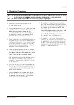
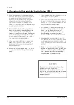
Precautions
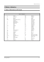
Reference Information
Specifications
Alignment and Adjustments
Circuit Operation Description
Troubleshooting
Exploded View and Parts List
Electric Parts List
Handling Description
Glossary
Wiring Diagram
Schematic Diagrams
1.
2.
3.
4.
5.
6.
7.
8.
9.
10.
11.
12.
Summary of Contents for PPM42S2X/XAA
Page 2: ...ELECTRONICS Samsung Electronics Co Ltd APR 2002 Printed in Korea AA82 ...
Page 10: ...3 2 Samsung Electronics MENO ...
Page 25: ...Circuit Operation Description Samsung Electronics 5 3 5 1 2 D PDP PS 42 BLOCK DIAGRAM ...
Page 38: ...Circuit Operation Description 5 16 Samsung Electronics 5 2 3 D DRIVER CIRCUIT DIAGRAM ...
Page 39: ...Circuit Operation Description Samsung Electronics 5 17 5 2 3 E DRIVER BOARD CONNECTOR LAYOUT ...
Page 40: ...Circuit Operation Description 5 18 Samsung Electronics ...
Page 41: ...Circuit Operation Description Samsung Electronics 5 19 ...
Page 42: ...Circuit Operation Description 5 20 Samsung Electronics ...
Page 43: ...Circuit Operation Description Samsung Electronics 5 21 ...
Page 44: ...Circuit Operation Description 5 22 Samsung Electronics ...
Page 45: ...Circuit Operation Description Samsung Electronics 5 23 ...
Page 46: ...Circuit Operation Description 5 24 Samsung Electronics ...
Page 47: ...Circuit Operation Description Samsung Electronics 5 25 ...
Page 48: ...Circuit Operation Description 5 26 Samsung Electronics ...
Page 49: ...Circuit Operation Description Samsung Electronics 5 27 ...
Page 50: ...Circuit Operation Description 5 28 Samsung Electronics ...
Page 51: ...Circuit Operation Description Samsung Electronics 5 29 ...
Page 52: ...Circuit Operation Description 5 30 Samsung Electronics ...
Page 82: ...Circuit Operation Description 5 60 Samsung Electronics ...
Page 83: ...Circuit Operation Description Samsung Electronics 5 61 ...
Page 84: ...Circuit Operation Description 5 62 Samsung Electronics MEMO ...
Page 93: ...Exploded View Parts List Samsung Electronics 7 1 7 Exploded View Parts List 7 1 PPM42S2X XAA ...
Page 106: ...Electrical Parts List 8 12 Samsung Electronics MEMO ...
Page 128: ...10 14 Samsung Electronics MEMO ...
Page 130: ...11 2 Samsung Electronics MENO ...
Page 133: ...Samsung Electronics Schematic Diagrams 12 3 TP01 12 3 SCALER3 3D COMB FILTER TP01 CVBS IN ...
Page 134: ...Schematic Diagrams 12 4 Samsung Electronics 12 4 SCALER4 VIDEO DECODER PIP FIRST IN OUTPUT ...
Page 135: ...Samsung Electronics Schematic Diagrams 12 5 12 5 SCALER5 VIDEO DA CON ...
Page 141: ...Samsung Electronics Schematic Diagrams 12 11 12 11 SOUND ...
Page 143: ...Samsung Electronics Schematic Diagrams 12 13 12 13 CONTROL REMOCON CONTROL REMOCON ...


