background image

Harman 5G NAD Design Specification Document


©  SAMSUNG Electronics Co., Ltd. Confidential & Proprietary 

/ 82


NAD SAMSUNG S5123 
Model SA-N9000 OEM D 


Hardware Guide


Version 1.3 (2020.12.03) 


Confidential and Proprietary – Samsung Electronics Co. & Harman


ⓒ 

2019 Samsung Electronics Co., Ltd. & Harman All rights reserved. 


Disclaimer: This  information is  confidential and  proprietary and  should  not  be  reproduced in  whole or  part  unless 
authorized in writing by the authorizing person of Samsung Electronics & Harman. 


Restricted Distribution: Not to be distributed to anyone who is not an employee of Automotive Electronics Business 
Team without the express approval of Samsung Electronics & Harman. 


Samsung Electronics Automotive Electronics Business Team


129,Samsung-ro, Yeongtong-gu, Suwon-si, Gyeonggi-do 16677 Korea 

Summary of Contents for S5123

Page 1: ...served Disclaimer This information is confidential and proprietary and should not be reproduced in whole or part unless authorized in writing by the authorizing person of Samsung Electronics Harman Restricted Distribution Not to be distributed to anyone who is not an employee of Automotive Electronics Business Team without the express approval of Samsung Electronics Harman Samsung Electronics Auto...

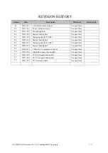
Page 2: ...ort band update Yoongoo Nam 0 5 2019 12 05 Pinmap update for TCAM2 Yoongoo Nam 0 6 2020 01 06 Support band update Yoongoo Nam 0 7 2020 02 24 Pinmap update for TCAM2 Yoongoo Nam 0 8 2020 03 10 Support band update Yoongoo Nam 0 9 2020 04 13 USB add CA combination update Yoongoo Nam 1 0 2020 05 06 Global sku support band update Yoongoo Nam 1 1 2020 10 16 LTE CA support band update Yoongoo Nam 1 2 202...

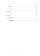
Page 3: ...on Interfaces 16 2 1 LGA Interface 16 2 2 LGA Interface guideline 29 2 2 1 ANT port 29 2 2 2 MIPI 29 2 2 3 PCIe 29 2 3 CP HW Revision 30 2 4 USB Interface 30 3 Power Interface 31 3 1 Power Interface 31 3 1 1 Overview 31 3 1 2 Input Power Supply Interface 32 3 1 3 Output Power Supply Interface 33 3 2 UART and SPI Interface 33 3 3 USIM Card Interface 34 3 4 Audio Interface 34 3 5 PCIe Interface 35 4...

Page 4: ... efficiency 50 4 5 1 2 VSWR 50 4 5 1 3 Isolation 50 4 5 1 4 Antenna line PCB drawing guide 50 4 5 2 Interface 51 4 5 3 GSM WCDMA LTE Antenna Requirements 52 4 6 Link budget 54 4 6 1 Antenna Design Indicators 54 4 7 PCB Recommendation 55 5 Electrical Features 57 5 1 About This Chapter 57 5 2 Absolute Ratings 57 5 3 Operating and Storage Temperatures and Humidity 57 5 4 Electrical Features of Applic...

Page 5: ...g 67 6 4 Label 68 6 5 Storage Guidelines 68 6 6 Moisture Sensitivity 68 7 Certification 69 7 1 Certifications 69 7 2 FCC IC Regulatory notices 69 8 Safety information 71 8 1 Safety information 71 9 Software information 72 9 1 AT Command 72 10 Acronyms and Abbreviations 73 ...

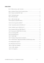
Page 6: ...on of the UART interface in the module with the host 33 Figure 3 3 Recommended connection of the SPI interface 33 Figure 3 4 Recommended circuit diagram of the PCM interface The module is used as PCM master 34 Figure 3 5 Recommended circuit of the PCIe interface CP Only 35 Figure 3 6 Recommended circuit of the PCIe interface eAP 36 Figure 3 7 Recommended circuit of the PCIe interface eAP DSDA 36 F...

Page 7: ...NAD 37 Table 4 2 Conducted Rx sensitivity of OEM NAD at 25 43 Table 4 3 Conducted Tx power of OEM NAD at 25 46 Table 4 4 Conducted ACLR value of OEM NAD at 25 48 Table 4 5 Requirements for GSM WCDMA LTE antenna 52 Table 4 6 Tx link budget MPR 0 54 Table 4 7 Recommend RF guide 56 Table 5 1 Absolute ratings 57 Table 5 2 Operating and storage temperatures and humidity 58 Table 5 3 Electrical features...

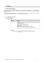
Page 8: ...ers to understand the interface specifications electrical features and related product guidelines of the SAMSUNG WAVE Network Access Device module 1 2 Function overview 1 2 1 Support Band Products Bands Global LTE FDD B1 B2 B3 B4 B5 B7 B8 B9 B10 B12 B13 B17 B18 B19 B20 B21 B25 B26 B28 B29 Rx B30 Rx B32 Rx B66 B71 LTE TDD B34 B38 B39 B40 B41 B42 WCDMA HSPA B1 B2 B3 B4 B5 B8 B19 GSM GPRS EDGE 850MHz...

Page 9: ... 7C 3C 7A 3A 3A 8A 3C 8A 3A 3A 19A 3A 3A 20A 3C 20A 3A 3A 28A 3C 28A 3C 32A 3C 38A 3A 5A 7A 3A 5A 40A 3A 7A 8A 3A 7A 20A 3A 7A 26A 3A 7A 28A 3A 7A 32A 3A 7A 42A 3A 8A 32A 3A 8A 38A 3A 8A 40A 3A 19A 42A 3A 20A 32A 3A 28A 38A 3A 28A 40A 3A 28A 42A 3A 40A 40A 3A 40C 3C 40A 4A 4A 5A 4A 5B 4A 4A 12A 4A 4A 13A 4A 4A 29A 4A 4A 30A 4A 4A 71A 4A 5A 30A 4A 12A 12A 4A 12B 4A 12A 30A 4A 29A 30A 5B 30A 5A 5A 4...

Page 10: ...3A 3A 7A 3C 7A 28A 7A 3C 28A 28A 3C 7A 3C 7A 32A 7A 3C 32A 3C 8A 38A 8A 3C 38A 3C 28A 38A 28A 3C 38A 3C 40C 3A 3A 42C 3A 5A 7A 7A 5A 3A 7A 7A 7A 7A 3A 5A 3A 5A 40A 40A 5A 3A 40A 40A 3A 7A 7A 8A 7A 7A 3A 8A 8A 3A 7A 7A 3A 7C 20A 7C 3A 20A 20A 3A 7C 3A 7A 7A 26A 7A 7A 3A 26A 26A 3A 7A 7A 3A 7C 28A 7C 3A 28A 28A 3A 7C 3A 7A 20A 32A 3A 7A 20A 42A 7A 3A 20A 42A 20A 3A 7A 42A 3A 8A 40C 8A 3A 40C 3A 19A ...

Page 11: ... 3A 42D 3A 19A 42D 19A 3A 42D 3A 28A 40D 28A 3A 40D 3A 28A 42D 28A 3A 42D 3A 40E 3A 42C 42C 3A 42E 4A 4A 5B 30A 5B 4A 4A 30A 5B 30A 66A 66A 66A 66A 5B 30A 5A 5A 66A 66B 66A 66B 5A 5A 66B 66A 5A 5A 5A 5A 66A 66C 66A 66C 5A 5A 66C 66A 5A 5A 5A 5A 66D 66D 5A 5A 5B 66A 66B 66A 66B 5B 66B 66A 5B 5B 66A 66C 66A 66C 5B 66C 66A 5B 8B 41D 21A 42E 28A 41C 42C 39A 42E 39C 41D 41D 39C 39C 42D 41C 41D 41D 41C ...

Page 12: ...Voltage DC 4 0 V to 4 4 V typical value is 4 2 V Antenna Interface antenna pad x 4 1 10 C 55 C This range is defined by 3GPP WAVE guarantees its modules to comply with all 3GPP standard and to have full functionality of the module with in this range 2 40 C 85 C WAVE guarantees full functionality within this range as well However there may possibly be some performance deviations in this extended ra...

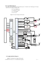
Page 13: ...er HB TX_TR_OUT_B21 B71 DPX AW79 PRX_TR_IN_B71 SAW Triplexer TX1_UHB LB MHB Triplexer TCXO 52MHz FBRX2 TX1_MHB1 TX2_LB2 TX_TR2_OUT_LB TX1_MHB2 Rx Mirconi Tx Mirconi x8 x4 TX_TR_OUT_N77_N78_B42 PRX_TR_IN_N77_N78_N79_B42 B21 B4374 B71 AT72B TX_TR2_OUT_N79 PRX_TR_IN_B7_B30_B38_B40_B41 PRX_TR_IN_B21_B32 DRX_TR_IN_LB DRX_TR_IN_B7_B30_B38_B40_B41 DRX_TR_IN_B21_B32 DRX_TR_IN_B2_B3_B9_B25_B39_DCS_PCS DRX_...

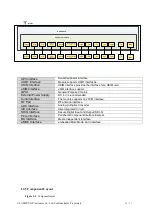
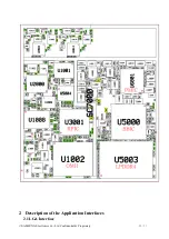
Page 14: ...RF Pad RF antenna interface ADC Interface Analog to Digital Converter I2C Interface Inter Integrated Circuit SDIO Interface Secure Digital Input and Output SD3 0 PCIe Interface Peripheral Component Interface Express MII Interface Media Independent Interface eMMC Interface embedded Multi Media Card Interface 1 2 5 Component Layout Figure 1 3 Componentlayout UART SPI GPIO Power Supply Wake up USIM R...

Page 15: ... SAMSUNG Electronics Co Ltd Confidential Proprietary 15 82 2 Description of the Application Interfaces 2 1 LGA Interface ...

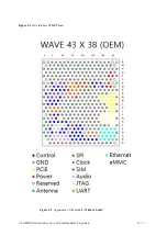
Page 16: ... SAMSUNG Electronics Co Ltd Confidential Proprietary 16 82 Figure 2 1 LGA Interface TOP View Figure 2 2 Appearance of the module Without Label ...

Page 17: ...Leave this pin open floating T35 VPH_PWR_5V 4 8 5 2 Power Input U34 VPH_PWR_5V 4 8 5 2 Power Input P13 VLDO2_CP_VDD180 1 8 Power Output VDD CP Power Output NAD_ECP_1V8 NAD_ECP_1V8 R21 VLDO10_CP_USIM0 1 8 Power Output USIM0 Power output NAD_SIM0_VCC NAD_SIM0_VCC R17 VLDO11_CP_USIM1 1 8 Power Output Reserved Leave this pin open floating NAD_SIM1_VCC Antenna Port C2 MAIN_ANT Prx MiMo 1 Antenna Port C...

Page 18: ...E2_REFCLK0_P 0 85 B PCIE REF CLKP Leave this pin open floating PCIE2_REFCLK0_P M34 PCIE2_RX0_N 0 85 O PCIE TXDN at CP side Leave this pin open floating PCIE2_RX0_N M36 PCIE2_RX0_P 0 85 O PCIE TXDP at CP side Leave this pin open floating PCIE2_RX0_P N33 PCIE2_TX0_N 0 85 I PCIE RXDN at CP side Leave this pin open floating PCIE2_TX0_N N35 PCIE2_TX0_P 0 85 I PCIE RXDP at CP side Leave this pin open fl...

Page 19: ...ay detect Need external PU 47k to NAD_ECP_1V8 Leave this pin open floating TRAY_DET_SIM1 CP_GPIO CV2X Interface L15 RAN_SYNC 1 8 O RAN SYNC for CV2X RAN_SYNC RAN_SYNC N17 GNSS_PPS 1 8 O GNSS PPS for CV2X Leave this pin open floating GNSS_PPS Debug Interface E8 RSV_CP_JTAG_TCK 1 8 I CPU JTAG TCK CP_JTAG_TCK CP_JTAG_TCK E6 RSV_CP_JTAG_TDI 1 8 I CPU JTAG TDI CP_JTAG_TDI CP_JTAG_TDI F11 RSV_CP_JTAG_TD...

Page 20: ...MC_D 6 I34 EMMC_D 7 1 8 B EMMC_D 7 Leave this pin open floating EMMC_D 7 G30 EMMC_NRESET 1 8 O EMMC_NRESET Leave this pin open floating EMMC_NRESET H29 EMMC_PWREN 1 8 O EMMC_PWREN Leave this pin open floating EMMC_PWREN I30 EMMC_RDQS 1 8 I EMMC_RDQS Leave this pin open floating EMMC_RDQS Ethernet Interface RGMII E32 XETH0_INTR 1 8 I XETH0_INTR Leave this pin open floating XETH0_INTR B29 XETH0_MDC ...

Page 21: ... GNSS_BLANK_RFIC I2C Interface I6 XUSI00_I2C_SDA 1 8 B I2C_SDA Leave this pin open floating XUSI00_I2C_SDA EXTCLK0 APGS I4 XUSI00_I2C_SCL 1 8 B I2C_SCL Leave this pin open floating XUSI00_I2C_SCL Q30 XUSI01_I2C_SDA 1 8 B I2C_SDA Leave this pin open floating XUSI01_I2C_SDA R29 XUSI01_I2C_SCL 1 8 B I2C_SCL Leave this pin open floating XUSI01_I2C_SCL O2 I2C1_SDA 1 8 B I2C1_SDA Leave this pin open flo...

Page 22: ...27 XCP_GPIO_58 1 8 B AP CP GPIO Leave this pin open floating AP_GPIO AP GPIO M32 AP_XEINT_0 1 8 I AP_GPIO NAD_PCIe_RSTn PCIE1 reset as NAD EP AP_GPIO G6 AP_XEINT_1 1 8 I AP_GPIO AP2CP_WAKEUP External AP sends an interrupt signal to wake up CP AP_GPIO G8 AP_XEINT_2 1 8 I AP_GPIO AP_CP2_DUMP_NOTI_n External AP sends an interrupt to notify AP active status to CP AP_GPIO G10 AP_XEINT_3 1 8 I AP_GPIO A...

Page 23: ... NAD internal PD 100k ohm C20 XCP_OM0 1 8 I XCP_OM0 Leave this pin open floating Need external PU 1k to NAD_ECP_1V8 B21 XCP_OM1 1 8 I XCP_OM1 Leave this pin open floating Leave this pin open floating B23 XCP_OM2 1 8 I XCP_OM2 Leave this pin open floating Need external PU 1k to NAD_ECP_1V8 Reserved Pins Q36 Reserved Reserved Leave this pin open floating Leave this pin open floating D21 Reserved Res...

Page 24: ...GND GND F27 GND GND GND GND F29 GND GND GND GND F37 GND GND GND GND G14 GND GND GND GND G16 GND GND GND GND G18 GND GND GND GND G20 GND GND GND GND G22 GND GND GND GND G24 GND GND GND GND G26 GND GND GND GND G28 GND GND GND GND H1 GND GND GND GND H3 GND GND GND GND H5 GND GND GND GND H11 GND GND GND GND H13 GND GND GND GND H15 GND GND GND GND H17 GND GND GND GND H19 GND GND GND GND H21 GND GND GND...

Page 25: ...ND GND GND K20 GND GND GND GND K22 GND GND GND GND K24 GND GND GND GND K26 GND GND GND GND K28 GND GND GND GND K30 GND GND GND GND K32 GND GND GND GND L1 GND GND GND GND L9 GND GND GND GND L11 GND GND GND GND L13 GND GND GND GND L17 GND GND GND GND L19 GND GND GND GND L21 GND GND GND GND L23 GND GND GND GND L25 GND GND GND GND L27 GND GND GND GND L29 GND GND GND GND L31 GND GND GND GND L37 GND GND...

Page 26: ...D GND GND GND P27 GND GND GND GND P29 GND GND GND GND P31 GND GND GND GND P33 GND GND GND GND P35 GND GND GND GND P37 GND GND GND GND Q4 GND GND GND GND Q28 GND GND GND GND R31 GND GND GND GND S4 GND GND GND GND S6 GND GND GND GND S8 GND GND GND GND S10 GND GND GND GND S12 GND GND GND GND S14 GND GND GND GND S16 GND GND GND GND S18 GND GND GND GND S20 GND GND GND GND S22 GND GND GND GND S24 GND GN...

Page 27: ... GND GND GND U30 GND GND GND GND U32 GND GND GND GND U36 GND GND GND GND V1 GND GND GND GND V3 GND GND GND GND V5 GND GND GND GND V7 GND GND GND GND V9 GND GND GND GND V11 GND GND GND GND V13 GND GND GND GND V15 GND GND GND GND V17 GND GND GND GND V19 GND GND GND GND V21 GND GND GND GND V23 GND GND GND GND V25 GND GND GND GND V27 GND GND GND GND V29 GND GND GND GND V31 GND GND GND GND V35 GND GND ...

Page 28: ...ing R1 NC NC Leave this pin open floating Leave this pin open floating R3 NC NC Leave this pin open floating Leave this pin open floating R35 NC NC Leave this pin open floating Leave this pin open floating R37 NC NC Leave this pin open floating Leave this pin open floating S2 NC NC Leave this pin open floating Leave this pin open floating S36 NC NC Leave this pin open floating Leave this pin open ...

Page 29: ...rt Figure 2 3 to improve RF performance Figure 2 3 Matching components at ANT port NAD LGA 100pF N C N C ANT 2 2 2 MIPI If TCU use Qorvo ANT switch USID pin of ANT switch should be connected to VIO pin to distinguish it from the ANT switch in NAD side 2 2 3 PCIe Place 220nF series capacitor close to MTK pin if they do not have any recommendation ...

Page 30: ...fidential Proprietary 30 82 2 3 CP HW Revision Figure 2 4 CP HW Revision 2 4 USB Interface S5123 chipset do not support USB The USB interface cannot be used in the NAD because related functions are not supported in the S5123 chipset ...

Page 31: ...cription Comment Q32 O34 R33 VPH_PWR PI Power supply input The rising time of VBAT must be greater than 100 µs Input power is 4 0 4 4 V The typical voltage is 4 2 V Those power pins are used for PMIC F15 VDD_1P8_AP PI Power supply input for PCIe PU It s for PCIe I F voltage level Supply same level with AP PCIe P13 VLDO2_CP_V DD180 PO Pin for external power output Module output power is 1 8 V This ...

Page 32: ...upply circuit of the VPH_PWR interface Figure 3 1 Recommended power circuit The UVLO circuit for the NAD prevents the device from malfunctioning at low input voltages and from excessive discharge of the power As VPH_PWR voltage is under UVLO threshold the NAD enters into UVLO state which forces the device to an inactive state until the VPH_PWR is high enough to allow the device to operate normal f...

Page 33: ...s 921600 bps 2764800 bps Table 3 3 UART interface signals Pin No Pin Name Pad Type Description Typ V P17 CP_UART_TX O UART transmit data output for debug 1 8 P15 CP_UART_RX I UART receive data input for debug 1 8 Figure 3 2 Recommended connection of the UART interface in the module with the host In addition the module provides a SPI interface Table 3 4 SPI interface signals Pin No Pin Name Pad Typ...

Page 34: ...io interface Table 3 6 Signals on the digital audio interface Pin No Pin Name Pad Type Description Typ V Comments B7 SPEECH_I2S _LRCK_CP I PCM interface L R Channel 1 8 The pin is output when the module is used as PCM master C8 SPEECH_I2S _D_IN_CP I PCM interface data in 1 8 B9 SPEECH_I2S _D_OUT_CP O PCM interface data out 1 8 C6 SPEECH_I2S _BCK_CP I PCM interface clock 1 8 The pin is output when ...

Page 35: ...ve inbound regions 4000 minimum region size 256 bytes maximum payload size 32 maximum outbound NP requests One virtual channel L1 sub states Dedicated Data Bus Interface DBI slave PCIe Interrupt Aggregator IA with sequencer It is recommended that thedifferential clock output signals of PCIeinterface should be connected as Figure 3 5 Two 220nF capacitors inner module are separately placed on the TX...

Page 36: ... SAMSUNG Electronics Co Ltd Confidential Proprietary 36 82 Hardware Guide Figure 3 6 Recommended circuit of the PCIe interface eAP Figure 3 7 Recommended circuit of the PCIe interface eAP DSDA ...

Page 37: ...x GSM 850 824 849 MHz 869 894 MHz GSM 900 880 915 MHz 925 960 MHz GSM 1800 1710 1785 MHz 1805 1880 MHz GSM 1900 1850 1910 MHz 1930 1990 MHz UMTS Band 1 1920 1980 MHz 2110 2170 MHz UMTS Band 2 1850 1910 MHz 1930 1990 MHz UMTS Band 3 1710 1785 MHz 1805 1880 MHz UMTS Band 4 1710 1755 MHz 2110 2155 MHz UMTS Band 5 824 849 MHz 869 894 MHz UMTS Band 8 880 915 MHz 925 960 MHz UMTS Band 19 830 845 MHz 875...

Page 38: ...803 MHz LTE Band 29 Downlink only 717 728 MHz LTE Band 30 Downlink only 2350 2360 MHz LTE Band 32 Downlink only 1452 1496 MHz LTE Band 66 1710 1780 MHz 2110 2200 MHz LTE Band 71 663 698 MHz 617 652 MHz LTE Band 34 2010 2025MHz 2010 2025MHz LTE Band 38 2570 2620 MHz 2570 2620 MHz LTE Band 39 1880 1920 MHz 1880 1920 MHz LTE Band 40 2300 2400 MHz 2330 2400 MHz LTE Band 41 2496 2690 MHz 2496 2690 MHz ...

Page 39: ...Mbps 5 76 Mbps EDGE DL 236 8 kbps UL 236 8 kbps Multi slot Class 12 GPRS DL 85 6 kbps UL 85 6 kbps Multi slot Class 12 GSM 9 6 kbps 14 4 kbps 5G Data service values may vary depending on the combination of support bands and CA The data service values shown in the table are the maximum data service values supported by the S5123 IC 1 5G NR Feature A Wavefrom DL CP OFDM only UL CP OFFM and DFT OFDM B...

Page 40: ... 23 dBm 2 dB for FDD LTE Band 19 Class 3 23 dBm 2 dB for FDD LTE Band 20 Class 3 23 dBm 2 dB for FDD LTE Band 21 Class 3 23 dBm 2 dB for FDD LTE Band 25 Class 3 23 dBm 2 dB for FDD LTE Band 26 Class 3 23 dBm 2 dB for FDD LTE Band 28 Class 3 23 dBm 2 dB for FDD LTE Band 34 Class 3 23 dBm 2 dB for FDD LTE Band 66 Class 3 23 dBm 2 dB for FDD LTE Band 71 Class 3 23 dBm 2 dB for TDD LTE Band 34 Class 3...

Page 41: ...ss 3 23 dBm 2 dB for n3 Class 3 23 dBm 2 dB for n5 Class 3 23 dBm 2 dB for n7 Class 3 23 dBm 2 dB for n8 Class 3 23 dBm 2 dB for n20 Class 3 23 dBm 2 dB for n25 Class 3 23 dBm 2 2 5 dB for n28 Class 3 23 dBm 2 dB for n38 Class 3 23 dBm 2 dB for n41 Class 3 23 dBm 2 dB for n66 Class 3 23 dBm 2 2 5 dB for n71 Class 3 23 dBm 2 3 dB for n77 Class 3 23 dBm 2 3 dB for n78 ...

Page 42: ...C DC_1A_n78C DC_3A_n77C DC_3A_n78C DC_19A_n77C DC_19A_n78C DC_21A_n77C DC_21A_n78C DC_28A_n77C DC_28A_n78C DC_1A_n28A n78A DC_3A_n28A n78A DC_7A_n28A n78ADC_1A 3A 5A_n78A DC_1A 3A 7A_n28A DC_1A 3A 7A_n78A DC_1A 3A 8A_n78A DC_1A 3A 19A_n77A DC_1A 3A 20A_n78A DC_1A 3A 28A_n77A DC_1A 3A 28A_n78A DC_1A 3C_n78A DC_1A 5A 7A_n78A DC_1A 7A 20A_n78A DC_3A 5A 7A_n78A DC_3A 7A 7A_n78A DC_3A 7C_n78A DC_3A 7A ...

Page 43: ...t indicates the receiver performance of the module The conducted receive sensitivity refers to the weakest signal that the module at the antenna port can receive The bit error rate BER must meet the 3GPP protocol requirements in the case of the minimum signal The 3GPP Protocol Claim column in Table 4 3 Table 4 4 lists the required minimum values and the Test Value column lists the tested values of...

Page 44: ...d Confidential Proprietary 44 82 Hardware Guide UMTS Band 2 BER 0 1 104 7 109 UMTS Band 3 BER 0 1 103 7 109 UMTS Band 4 BER 0 1 106 7 109 UMTS Band 5 BER 0 1 104 7 109 UMTS Band 8 BER 0 1 103 7 109 UMTS Band 19 BER 0 1 106 7 109 ...

Page 45: ... AUX 10 MHz 94 99 LTE Band 18 RX Main AUX 10 MHz 97 99 LTE Band 19 RX Main AUX 10 MHz 97 99 LTE Band 20 RX Main AUX 10 MHz 94 100 LTE Band 21 RX Main AUX 10 MHz 97 99 LTE Band 25 RX Main AUX 10 MHz 93 5 100 LTE Band 26 RX Main AUX 10 MHz 94 5 100 LTE Band 28 RX Main AUX 10 MHz 95 5 100 LTE Band 29 RX Main AUX 10 MHz LTE Band 30 RX Main AUX 10 MHz LTE Band 32 RX Main AUX 10 MHz LTE Band 34 RX Main ...

Page 46: ...e from the minimum power to the maximum power Table 4 6 list the required ranges of the conducted Adjacent Channel Leakage power Ratio ALCR criteria and measurements of the module under 4 V voltage and normal temperature Table 4 3 Conducted Tx power of OEM NAD at 25 Item 3GPP Protocol Claim dBm Test Value dBm Min Typ Max GSM 850 GMSK 1Tx Slot 31 35 31 33 35 8PSK 1Tx Slot 24 30 24 27 30 GSM 900 GMS...

Page 47: ...3 21 25 21 23 25 LTE Band 17 21 25 21 23 25 LTE Band 18 21 25 21 23 25 LTE Band 19 21 25 21 23 25 LTE Band 20 21 25 21 23 25 LTE Band 21 21 25 21 23 25 LTE Band 25 21 25 21 23 25 LTE Band 26 21 25 21 23 25 LTE Band 28 21 25 21 23 25 LTE Band 29 Downlink only LTE Band 30 Downlink only LTE Band 32 Downlink only LTE Band 34 21 25 21 23 25 LTE Band 38 21 25 21 23 25 LTE Band 39 21 25 21 23 25 LTE Band...

Page 48: ...10MHz Offset 42 2 UMTS Band 2 Adjacent channel Leakage Power_Ratio 10MHz Offset 42 2 UMTS Band 3 Adjacent channel Leakage Power_Ratio 10MHz Offset 42 2 UMTS Band 4 Adjacent channel Leakage Power_Ratio 10MHz Offset 42 2 UMTS Band 5 Adjacent channel Leakage Power_Ratio 10MHz Offset 42 2 UMTS Band 8 Adjacent channel Leakage Power_Ratio 10MHz Offset 42 2 UMTS Band 19 Adjacent channel Leakage Power_Rat...

Page 49: ... Ratio_RB_LOW_UTRA 35 2 LTE Band 18 Adjacent Channel Leakage power Ratio_RB_LOW_UTRA 35 2 LTE Band 19 Adjacent Channel Leakage power Ratio_RB_LOW_UTRA 35 2 LTE Band 20 Adjacent Channel Leakage power Ratio_RB_LOW_UTRA 35 2 LTE Band 21 Adjacent Channel Leakage power Ratio_RB_LOW_UTRA 35 2 LTE Band 25 Adjacent Channel Leakage power Ratio_RB_LOW_UTRA 35 2 LTE Band 26 Adjacent Channel Leakage power Rat...

Page 50: ...anding Wave Ratio SWR VSWR is a function of the reflection coefficient which describes the power reflected from the antenna 4 5 1 3 Isolation Antenna to antenna isolation is a measure of how tightly coupled antennas are Typically antenna isolation is measured for antennas on the same product that is the isolation between a smartphone GPS and Wi Fi antenna for instance When specified in this manner...

Page 51: ...arious interference sources such as the LCD CPU audio circuits and power supply All the interference sources emit interference signals that affect the normal operation of the module For example the module sensitivity can be decreased due to interference signals Therefore during the design need to consider how to reduce the effects of interference sources on the module It is recommended to take the...

Page 52: ... MHz in WCDMA LTE Band 1 140 MHz in WCDMA LTE Band 2 170 MHz in WCDMA LTE Band 3 445 MHz in WCDMA LTE Band 4 70 MHz in WCDMA LTE Band 5 80 MHz in WCDMA LTE Band 8 60 MHz in WCDMA LTE Band 19 190 MHz in LTE Band 7 130 MHz in LTE Band 9 460 MHz in LTE Band 10 47 MHz in LTE Band 12 41 MHz in LTE Band 13 42 MHz in LTE Band 17 60 MHz in LTE Band 18 71 MHz in LTE Band 20 63 MHz in LTE Band 21 145 MHz in...

Page 53: ...d 9 460 MHz in LTE Band 10 47 MHz in LTE Band 12 41 MHz in LTE Band 13 42 MHz in LTE Band 17 60 MHz in LTE Band 18 71 MHz in LTE Band 20 63 MHz in LTE Band 21 145 MHz in LTE Band 25 80 MHz in LTE Band 26 100 MHz in LTE Band 28 11 MHz in LTE Band 29 10 MHz in LTE Band 30 44 MHz in LTE Band 32 15 MHz in LTE Band 34 50 MHz in LTE Band 38 40 MHz in LTE Band 39 100 MHz in LTE Band 40 194 MHz in LTE Ban...

Page 54: ... SAMSUNG Electronics Co Ltd Confidential Proprietary 54 82 Hardware Guide 4 6 Link budget 4 6 1 Tx link budget Table 4 6 Tx link budget MPR 0 ...

Page 55: ...PCIE line are not isolated and it will cause cross talk Layer 1 Layer 2 Layer 3 RF Signals are not shielded with GND There are not GND Via next to the signal lines This Impedance mismatch causes High insertion loss RF Signals and too many digital analog lines are not isolated Cross talk and Impedance mismatch There are line width discontinuity and Impedance mismatch This Impedance mismatch causes ...

Page 56: ...ld outline of PCB GND shielding and more GND Vias can prevent the board from EMC issue RE ESD noise protect etc Layer 1 Layer 2 Layer 3 Clock line is not shielded with GND This can be a noise source and cause RX sensitivity interference Signal Vias are not shielded with GND These can cause cross talk RX sensitivity interference ...

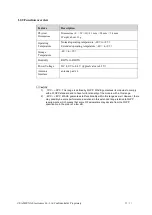
Page 57: ...able 5 1 lists the absolute ratings for the module Using the module beyond these conditions may result in permanent damage to the module Table 5 1 Absolute ratings Symbol Specification Min Max Unit VBAT External power voltage 0 3 4 5 V 5 3 Operating and Storage Temperatures and Humidity Table 5 2 lists the operating and storage temperatures and humidity for the WAVE LGA module Table 5 2 Operating ...

Page 58: ...l GPIO Voltage 5 5 Power Supply Features 5 5 1 Input Power Supply Table 5 4 lists the requirements for input power of the NAD LGA module Table 5 4 Requirements for input power Parameter Min Typ Max Ripple Unit VPH_PWR 4 0 4 2 4 4 0 05 V The minimum voltage of VBAT can extend to 3 6 V under this condition only ensure the module will not restart but the characteristics cannot be guaranteed Figure 5 ...

Page 59: ...er Band 3 360 mA 1 dBm Tx Power 540 10 dBm Tx Power 950 Max Tx Power Band 4 430 mA 1 dBm Tx Power 560 10 dBm Tx Power 1000 Max Tx Power Band 5 430 mA 1 dBm Tx Power 560 10 dBm Tx Power 1000 Max Tx Power Band 7 430 mA 1 dBm Tx Power 560 10 dBm Tx Power 1000 Max Tx Power Band 8 360 mA 1 dBm Tx Power 550 10 dBm Tx Power 900 Max Tx Power Band 9 360 mA 1 dBm Tx Power 540 10 dBm Tx Power 950 Max Tx Powe...

Page 60: ...wer Band 18 360 mA 1 dBm Tx Power 540 10 dBm Tx Power 950 Max Tx Power Band 19 430 mA 1 dBm Tx Power 560 10 dBm Tx Power 1000 Max Tx Power Band 20 430 mA 1 dBm Tx Power 560 10 dBm Tx Power 1000 Max Tx Power Band 21 430 mA 1 dBm Tx Power 560 10 dBm Tx Power 1000 Max Tx Power Band 25 360 mA 1 dBm Tx Power 550 10 dBm Tx Power 900 Max Tx Power Band 26 360 mA 1 dBm Tx Power 540 10 dBm Tx Power 950 Max ...

Page 61: ...r 550 10 dBm Tx Power 900 Max Tx Power Band 34 360 mA 1 dBm Tx Power 540 10 dBm Tx Power 950 Max Tx Power Band 38 370 mA 1 dBm Tx Power 520 10 dBm Tx Power 950 Max Tx Power Band 39 350 mA 1 dBm Tx Power 400 10 dBm Tx Power 900 Max Tx Power Band 40 360 mA 1 dBm Tx Power 540 10 dBm Tx Power 950 Max Tx Power Band 41 370 mA 1 dBm Tx Power 520 10 dBm Tx Power 950 Max Tx Power Band 42 350 mA 1 dBm Tx Po...

Page 62: ...x Power Band 2 360 mA 1 dBm Tx Power 540 10 dBm Tx Power 950 Max Tx Power Band 3 430 mA 1 dBm Tx Power 560 10 dBm Tx Power 1000 Max Tx Power Band 4 360 mA 1 dBm Tx Power 550 10 dBm Tx Power 900 Max Tx Power Band 5 360 mA 1 dBm Tx Power 540 10 dBm Tx Power 950 Max Tx Power Band 8 370 mA 1 dBm Tx Power 520 10 dBm Tx Power 950 Max Tx Power Band 19 370 mA 1 dBm Tx Power 520 10 dBm Tx Power 950 Max Tx ...

Page 63: ... 200 mA 10 1 Up 1 Down 280 2 Up 1 Down 630 4 Up 1 Down GPRS 900 320 mA 5 1 Up 1 Down 450 2 Up 1 Down 650 4 Up 1 Down 200 mA 10 1 Up 1 Down 280 2 Up 1 Down 630 4 Up 1 Down GPRS 1800 320 mA 5 1 Up 1 Down 450 2 Up 1 Down 650 4 Up 1 Down 200 mA 10 1 Up 1 Down 280 2 Up 1 Down 630 4 Up 1 Down GPRS 1900 320 mA 5 1 Up 1 Down 450 2 Up 1 Down 650 4 Up 1 Down 200 mA 10 1 Up 1 Down 280 2 Up 1 Down 630 4 Up 1 ...

Page 64: ...age or ESD To protect the circuit from ESD TVS Diode should be added to RF antenna port USIM USB port An integrated ground plane is necessary for EMC design To protect sensitive circuitry from electrical overstress failures ESD protection diodes are connected to each signal line between the interface connector and the NAD Module In the factory line the operator must remove the element that the ESD...

Page 65: ... SAMSUNG Electronics Co Ltd Confidential Proprietary 65 82 Hardware Guide 6 Package Information 6 1 Dimensions Figure 6 1 Dimension ...

Page 66: ...ntial Proprietary 66 82 Hardware Guide 6 2 Shield can information This chapter describe shield can information for WAVE NAD Shield can material i Frame C7701 1 2H T0 20 Nickel Silver ii Cover SUS304 Stainless Figure 6 2 Shield can cover ...

Page 67: ... SAMSUNG Electronics Co Ltd Confidential Proprietary 67 82 Hardware Guide 6 3 Packaging Figure 6 3 Packaging ...

Page 68: ...low 40 C and relative humidity below 90 to ensure weldability 6 6 Moisture Sensitivity Moisture Sensitivity Level 3 After unpacking the module shall be assembled within 168 hours under environmental conditions where the temperature is less than 30 C and the relative humidity is less than 60 If the above conditions cannot be met the module shall be used after baking Baking is recommended for about ...

Page 69: ... mobile or fixed devices incorporating this module series are authorized to use the FCC Grants of the for their own final products according to the conditions referenced in the certificates The FCC Label shall in the above case be visible from the outside or the host device shall bear a second label stating Contains FCC ID T8GSAN9000 IMPORTANT Manufacturers of portable applications incorporating t...

Page 70: ...rence that may cause undesired operation of the device Radio Frequency RF Exposure Information The radiated output power of the Samsung Electronics Co Harman Cellular Module is below the Innovation Science and Economic Development Canada ISED radio frequency exposure limits The Samsung Electronics Co Harman Cellular Module should be used in a manner such that the potential for human contact during...

Page 71: ...ins lors du fonctionnement normal Ce périphérique a été évalué et démontré conforme aux limites d exposition aux fréquences radio RF d IC lorsqu il est installé dans des produits hôtes particuliers qui fonctionnent dans des conditions d exposition à des appareils mobiles les antennes se situent à plus de 20 centimètres du corps d une personne Ce périphérique est homologué pour l utilisation au Can...

Page 72: ...he product unless it is the authorized person in charge The warranty for the product may be difficult when arbitrarily disassembled It is recommended that you follow the instructions of the Hardware Guide for the correct use of the product This product must supply stabilized voltage sources and wiring must comply with security and fire prevention regulations Because electrostatic discharge may dam...

Page 73: ...o Ltd Confidential Proprietary 73 82 Hardware Guide 9 Software information 9 1 AT Command Table 8 1 AT Command List Command TX RX H W REV AT HWREV HWREV 6 SKU AT CPSKU CPSKU 0 NAD S W Version AT CGMR S5123_WAVEM_SGC_xxxxxxx ...

Page 74: ...Block Error Rate BIOS Basic Input Output System CA Carrier Aggregation CCC China Compulsory Certification CE European Conformity CMOS Complementary Metal Oxide Semiconductor CPU Central Processing Unit CS Circuit Switched CUST Customer NAD DVDD Digital power source DC Direct Current DCE Data Communication Equipment DCS Digital Cellular System DL Down Link DMA Direct Memory Access DNL Differential ...

Page 75: ...CF Global Certification Forum GMSK Gaussian Minimum Shift frequency Keying GPIO General Purpose I O GPRS General Packet Radio Service GPS Global Positioning System GSM Global System for Mobile Communication GLONASS Global Navigation Satellite System GNSS Global Navigation Satellite System HBM Human Body Model HSDPA High Speed Downlink Packet Access HSPA High Speed Packet Access HSPA Enhanced High ...

Page 76: ... MIMO Multiple Input Multiple Output MPR Maximum Power Reduction MO Mobile Originated MT Mobile Terminated NC Not Connected NR New Radio NSMD Non Solder Mask Defined OC Open Collector PA Power Amplifier PD Pull Down resistor PCB Printed Circuit Board PCL Power Control Level PCM Pulse Code Modulation PCS Personal Communications System PDU Protocol Data Unit PID Product Identity PMU Power Management...

Page 77: ...urface Mounting Technology TBD To Be Determined TCU Telematics Control Unit TDD Time Division Duplex TIS Total Isotropic Sensitivity TTFF Time to First Fix TVS Transient Voltage Suppressor TX Transmit Direction UART Universal Asynchronous Receiver Transmitter UL Up Link UMTS Universal Mobile Telecommunications System USB Universal Serial Bus USIM Universal Subscriber Identity Module V2X Vehicle to...

Page 78: ...B_TX GNSS_UART_TX D27 GNSS_CHUB_RX GNSS_UART_RX D23 GNSS_DEBUG_RX GNSS_UART_CTS C22 GNSS_DEBUG_TX GNSS_UART_RTS I6 Reserved XUSI00_I2C_SDA I4 Reserved XUSI00_I2C_SCL Q30 Reserved XUSI01_I2C_SDA R29 Reserved XUSI01_I2C_SCL O2 Reserved I2C1_SDA P11 Reserved I2C1_SCL F17 CP2AP_NOTIFY_ACTIVE XCP_GPIO3_CPALV F19 CP_AP_WAKE XCP_GPIO4_CPALV R5 CP2MCU_WAKEUP XCP_GPIO_23 H7 Reserved XCP_GPIO_46 I8 Reserved...

Page 79: ...eserved CP_SPI1_CLK_FLASH N5 Reserved CP_SPI1_WPN_FLASH Q36 FromAP_TCXO_REQ Reserved D21 SD_ENABLE Reserved V33 GPIO_CV2X_TX_RX Reserved 2020 03 06 v08 1 p 8 RF support band update NA n78 removed ECE n79 removed CHN WCDMA B5 add TDD B34 B39 removed ROW WCDMA B3 B5 add 5G n3 n8 add Global WCDMA B3 add 5G n8 add 2 p 9 CA combination support band removed 7A 20A 38A 7A 28A 38A 3 p 12 Power voltage cha...

Page 80: ...mperature revised 20 C 55 C 10 C 55 C 4 p 9 7A 7A 66A 7A 66A 66A 7A 7A 66A 66A 7C 66A 7C 66A 66A 7A 12A 66A 7A 12B 66A B66 SCC only support ULCA 8B 41A 42C 40D Not offered 2020 12 01 v12 1 p 8 NA CHN ECE Skew removed p 9 LTE CA list update 2A 28A 4A 28A 20A 42A 20A 42A 42A 32A 42A 39A 42A 39A 42C 39A 42D 39A 42E 39C 42A 39C 42D 2A 4A 28A 3A 3A 7A 7A 8A 3A 20A 42A 3A 32A 42A 7A 20A 42A 20A 32A 42A ...

Reviews: