N
GSM TELEPHONE
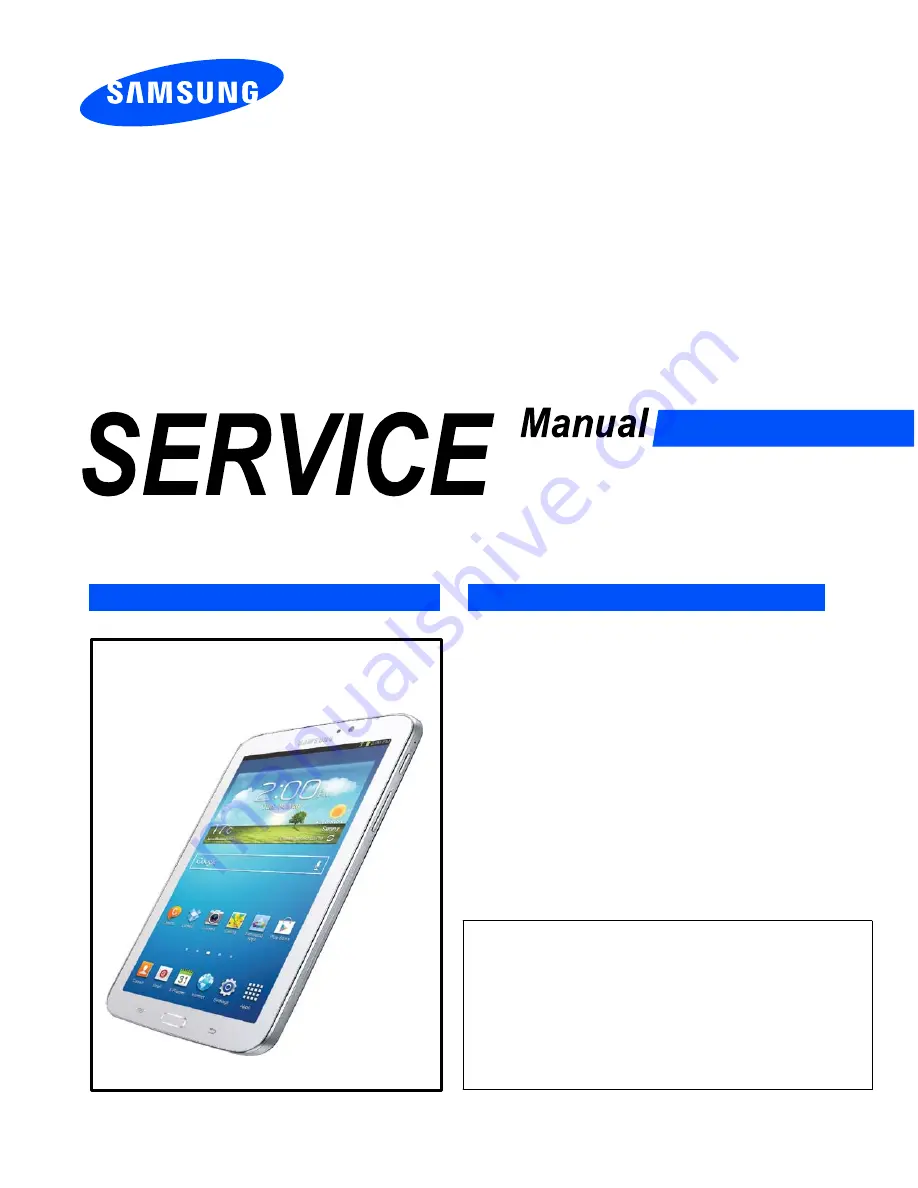
SM-T211
1.
Safety Precautions
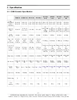
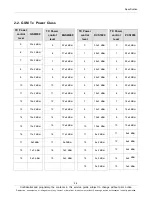
2.
Specification
3.
Product Function
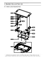
4.
Exploded View and Parts list
5.
MAIN Electrical Parts List
6.
Level 1 Repair
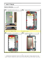
7.
Level 2 Repair
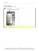
8.
Level 3 Repair
9.
Reference data
Notice: All functionality, features, specifications, and
other product information provided in this document,
including but not limited to, benefits, design, pricing,
components, performance, availability, and capabiliti
-es of the product are subject to change without
notice. Samsung reserves the right to alter this doc
-ument or the product described herein at anytime,
without obligation to provide notification of such
changes.
GSM TELEPHONE
CONTENTS