

Reviews:
No comments
Related manuals for Kontron COMe Eval Carrier2 T6
Q7-BASE
Brand: ADLINK Technology Pages: 52
PBN-9007
Brand: Arbor Technology Pages: 14
IP417
Brand: IBASE Technology Pages: 30
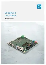
MB-COME6-4
Brand: TQ Pages: 30
21990-401
Brand: nvent Pages: 36
A203
Brand: Leetop Pages: 29
SMARC T335 Series
Brand: Embedian Pages: 129
TQMa65 Series
Brand: TQ Pages: 38
101459
Brand: Ironton Pages: 12
APC8620 Series
Brand: Acromag Pages: 21
Kria K26 SOM
Brand: Xilinx Pages: 59
JB-FLDSC-NAO-02
Brand: Diamond Systems Pages: 36
Actuated Tailboard
Brand: REDEKOP Pages: 12
MS-9988
Brand: MSI Pages: 60
MicroMod DEV-18575
Brand: sparkfun Pages: 33
AAEON UP 4000 M.2 Plus
Brand: Asus Pages: 34
CNF24
Brand: Samsung Pages: 63

CBK-HD02
Brand: Sony Pages: 10


