background image

SERVICE MANUAL

Digital Disc Camera

IDC-1000ZE

IDC-1000ZU

(Product Code : 126 250 01)
(U.K.)

(Product Code : 126 250 03)
(U.S.A.)
(Canada)

Contents
1. iD PHOTO DISC ........................................................ 2
2. OUTLINE OF iD FORMAT DISC DRIVE CIRCUIT .... 4
3. OUTLINE OF CIRCUIT DESCRIPTION .................... 9
4. DISASSEMBLY ........................................................ 20
5. ELECTRICAL ADJUSTMENT .................................. 24
6. MAC ADDRESS ....................................................... 29
7. TROUBLESHOOTING GUIDE ................................. 30

The components designated by a symbol (   !   ) in this schematic diagram designates components whose value are of

special significance to product safety. Should any component designated by a symbol need to be replaced, use only the part

designated in the Parts List. Do not deviate from the resistance, wattage, and voltage ratings shown.

CAUTION : Danger of explosion if battery is incorrectly replaced.

Replace only with the same or equivalent type recommended by the manufacturer.
Discard used batteries according to the manufacturer’s instructions.

NOTE : 1. Parts order must contain model number, part number, and description.

2. Substitute parts may be supplied as the service parts.
3. N. S. P. : Not available as service parts.

Design and specification are subject to change without notice.

SX111/E, EX, U

REFERENCE No. SM5310255

FILE NO.

PRODUCT SAFETY NOTICE

IDC-1000ZEX

(Product Code : 126 250 02)
(Europe)
(General PAL area)

8. PARTS LIST ............................................................. 31
    ACCESSORIES & PACKING MATERIALS ............. 31
    CABINET & CHASSIS PARTS 1 ............................. 32
    CABINET & CHASSIS PARTS 2 ............................. 34
    CABINET & CHASSIS PARTS 3 ............................. 35
    ELECTRICAL PARTS .............................................. 36
CIRCUIT DIAGRAM (Refer to the separate volume)

CAUTION

This product utilizes a laser.
The adjustment other than those specified herein may result in hazardous radiation exposure.

Summary of Contents for IDC-1000ZE iDshot

Page 1: ...ion if battery is incorrectly replaced Replace only with the same or equivalent type recommended by the manufacturer Discard used batteries according to the manufacturer s instructions NOTE 1 Parts order must contain model number part number and description 2 Substitute parts may be supplied as the service parts 3 N S P Not available as service parts Design and specification are subject to change ...

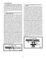
Page 2: ...ethod does not re sult in any changes to the physical nature of the disc This means that stable characteristics can be maintained for re spected disc writing operations 1 3 CAD ULTRA HIGH MAGNETIC RESOLUTION METHOD In order to play back the extremely small marks which have been recorded using laser pulse magnetic field modulation the iD Photo disc uses a ultra high magnetic resolution method which...

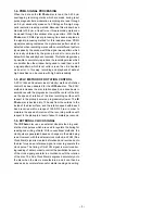
Page 3: ...hod of rotation control has been adopted for the iD Photo disc The ZCLV method increases the disc rotation speed on a zone basis in accordance with the progression toward the center of the disc as the speed of rotation of the disc recording surface with respect to the pickup becomes progressively slower The iD Photo disc is devided into 12 bands from the outside to the inside of the disc surface a...

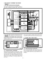
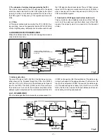
Page 4: ... EJLK MH MH MC1 Amplitude limitation circuit To the magnetic head Fig 3 MC2 WRPROT CARTRG PUINI SPDLW SPDLU SPDLV SPDLCOM Disc write protect detection switch Disc setting detection switch Pick up location detection sensor S8003 S8004 D8003 To the spindle motor The ascent and descent condition of the magnetic head is being watched with the magnetic head up and down sensor WDTX reverse of WDT WDT A ...

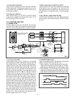
Page 5: ...hich is built into the ASIC IC402 This controls the tracking actuator and the thread actuator of the pickup in order to carry out rotation offset track ing control Fig 4 Fig 5 H F C D B A E G IC815 BD6603KVT IC835 AD8532 Buf TES TZC TZC tracking zero cross FES PWM 5 6 TRKFTRKR PWM 1 2 SLDFSLDR 2 IN1F 3 IN1R 36 IN4F 35 IN4R H1F OUT 9 H1R OUT 7 H4F OUT 40 H4R OUT 42 Tracking error signal observation...

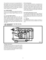
Page 6: ...through the peak hold and bottom hold circuits and are input to the DSP of the ASIC IC402 where A D conversion is carried out At the DSP of the ASIC IC402 the D A value of the signal FCLKGC which has had the control voltage adjusted by the VCA IC853 is changed so that the FCM level is set to the level which is necessary for the FCLKNP and FCLKPP signals to be generated Furthermore DSP of the ASIC ...

Page 7: ...r other high frequency interference can become mixed in with the FCM signal or the address signal These LC filters remove almost all of the signal components which are at 20 MHz or above leaving just the base frequencies 2 3 MHz for the FCM and address signals 5 Peak hold for FCM signal and bottom hold circuit These circuits use the amplitude modulation of the FCM sig nal to hold the peak level an...

Page 8: ...nt FCM cycle 26 6 µs Accodingly the rotation becomes faster as tracking moves toward the center of the disc Fig 10 The signals from the sensors I J are pre amplified by the gain amplifier and then pass through the AGC equalizer of the SSI IC831 and are then input to the RF signal terminal of the ASIC IC402 The AGC control signal AGCOFFH from the ASIC IC402 is modulated to control the on off status...

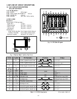
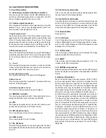
Page 9: ...RCUIT DESCRIPTION Around CCD block 1 IC Configuration IC903 ICX267 CCD imager IC902 IC904 IC908 74ACT04MTC H driver IC907 CXD3400N V driver IC905 AD9803 CDS AGC A D converter 2 IC903 CCD Structure Interline type CCD image sensor Optical size 1 2 type Effective pixels 1392 H 1040 V Pixels in total 1434 H 1050 V Actual pixels 1360 H 1024 V Optical black Horizontal H direction Front 2 pixels Rear 40 ...

Page 10: ...the reset gate clock 4 IC905 CDS AGC Circuit and A D Converter The video signal which is output from the CCD is input to Pin 30 of IC905 There are S H blocks inside IC905 generated from the XSHP and XSHD pulses and it is here that CDS correlated double sampling is carried out After passing through the CDS circuit the signal passes through the AGC amplifier It is A C converted internally into a 10 ...

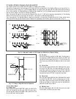
Page 11: ...lower The equivalent circuit for the output circuit is shown in Fig 1 7 H1 H2 H1 H2 H1 HOG RG CCD OUT PD Floating diffusion 1 H1 H2 H1 H2 H1 HOG RG CCD OUT PD 2 H1 H2 H1 H2 H1 HOG RG CCD OUT 3 H1 H2 RG CCD OUT 3 5V 0V 3 5V 0V 15 5V 12V Black level RG pulse peak signal Signal voltage 1 2 3 6 Lens drive block 6 1 Shutter drive The shutter drive signal SHUTTER which is output by the ASIC and the aper...

Page 12: ...dio This circuit converts the audio signals analog signals from the microphone to 8 bit digital signals 1 9 8 bit A D circuit Audio The audio signals which were converted to digial form by the 8 bit A D circuit are temporarily to a sound buffer and then recorded in the SSFDC card During playback the 8 bit D A circuit converts these signals into analog audio signals 1 10 Sound buffer Audio memory 1...

Page 13: ...way as for EE the data is then sent to the SDRAM after which D A conversion is carried out inside the ASIC and then the data is sent to the LCD panel and displayed The LCD driver is converted Y C signals to RGB signals from ASIC and these RGB signals and the control signal which is output by the LCD driver are used to drive the LCD panel The RGB signals are 1H transposed so that no DC compo nent i...

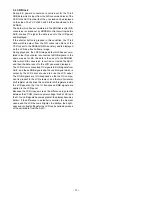
Page 14: ...ed to Pin 26 of IC501 so that PWM control can be carried out 1 5 Digital 2 4 V System Power Output IC501 CH3 is output It is used for core power supply of cam era ASIC Feedback for output voltage is provided to Pin 11 of IC501 so that PWM control can be carried out 1 6 Motor 5 V Power Output IC501 CH4 is output It is used for lens circuit power supply Feedback for output voltage is provided to Pin...

Page 15: ...re output 1 3 4 9 V System Power Output CH1 is output It is divided 4 9 V D and 4 9 V A 4 9 V A is mainly used for laser power supply Feedback for output voltage is provided to Pin 29 of IC521 so that PWM control can be carried out 1 4 Analog 3 1 V System Power Output CH2 is output It is used for disc servo etc of analog circuit power supply Feedback for output voltage is provided to Pin 26 of IC5...

Page 16: ...ting current which is generated at the secondary side of T5401 is rectified to produce a high voltage direct current and is accumulated at electrolytic ca pacitor C5050 on the PW1 circuit board 1 6 Voltage monitoring circuit This circuit is used to maintain the voltage accumulated at C5050 at a constance level After the charging voltage is divided and converted to a lower voltage by R5417 and R541...

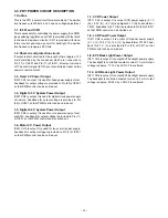
Page 17: ...CIRCUIT DESCRIPTION 1 Configuration and Functions For the overall configuration of the SY1 circuit board refer to the block diagram The configuration of the SY1 circuit board centers around a 8 bit microprocessor IC301 The 8 bit microprocessor handles the following functions 1 Operation key input 2 Mode LCD display 3 Clock control 4 Power ON OFF 5 Storobe charge control Key matrix input SI 26 13 1...

Page 18: ...C TEST 1 AVSS BATTERY O O O O O I Key matrix output LCD monitor power ON OFF signal H ON ASIC reset signal L Reset output ASIC test signal A D converter GND power terminal Battery voltage input analog input ASIC reset control signal Table 4 1 8 bit Microprocessor Port Specification 89 JOG R I Jog right rotation 90 JOG L I Jog left rotation 0 1 2 3 0 1 2 3 SCAN OUT SCAN IN LEFT 1st STILL IMAGE SET ...

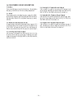
Page 19: ...ry is attached a regulated 3 2 V voltage is normally input to the 8 bit microprocessor IC301 by IC302 so that clock counting and key scanning is carried out even when the power switch is turned off so that the camera can start up again When the battery is removed the 8 bit micro processor operates in sleep mode using the backup battery At this time the 8 bit microprocessor only carries out clock c...

Page 20: ...t 17 Cabinet lens R 18 Connector 19 FPC 20 Screw 1 7 x 2 5 21 SY2 board 22 Screw 1 7 x 3 5 23 Flexible PWB unit 24 Two FPCs 25 Connector 26 Cabinet jog B 27 Two screws 1 7 x 2 5 28 Button AWB 29 Five screws 1 7 x 4 30 SY4 board 31 Two screws 1 7 x 4 32 Holder zoom A 33 Push the button 34 Three screws 1 7 x 2 5 35 Screw 1 7 x 5 36 Holder flash B 37 Two screws 1 7 x 4 38 Screw 1 7 x 6 39 Cabinet bot...

Page 21: ... dec LCD 16 FPC 17 Unit flexible PWB 18 FPC 24 Two screws 1 7 x 2 5 25 Holder brind 26 Two screws 1 7 x 3 5 27 Holder SY 28 Screw 1 7 x 2 29 Holder heat sink 30 Screw 1 7 x 3 5 31 SY3 board 32 Screw 1 7 x 3 5 33 Two connectors 34 ST1 board 35 Two screws 1 7 x 3 5 36 Screw 1 7 x 4 0 37 Holder lens MO 19 Connector 20 LCD 21 FPC 22 Flexible flat cable 23 SY1 board E G G F F E 1 2 3 4 5 6 7 8 9 10 11 ...

Page 22: ... 5 5 Two screws 1 7 x 3 5 6 Two screws 1 7 x 4 7 FPC 8 Three connectors 9 CA2 board 10 Five screws 1 4 x 2 5 11 Cover mecha protective housings 12 Two screws 1 7 x 3 5 13 Holder lens back 14 Two screws 1 7 x 3 5 15 Two screws 1 7 x 2 16 Holder lens mecha 17 Heat sink A 17 1 1 2 3 4 4 5 5 9 6 6 7 8 10 10 11 12 13 14 15 16 ...

Page 23: ...top 8 Screw 1 7 x 2 5 9 Unit flexible PWB 10 Two screws 2 0 x 3 5 11 Holder lens front 12 Shield tape 13 Screw 2 x 2 5 14 Two screws 2 x 6 15 CA1 board 16 Screw 2 0 x 3 5 17 Holder battery C 18 Two screws 1 7 x 3 19 SY5 board 18 19 17 16 15 12 13 14 3 1 2 4 5 7 9 8 6 11 10 PW2 board CA3 board PW1 board SY5 board SY4 board SY2 board SY3 board ST1 board CA2 board CA1 board MC3 board SY1 board ...

Page 24: ...or or high color display IEEE1394 port when carrying out IEEE1394 operation com pliance checks 2 Installing calibration software 1 Insert the calibration software installation diskette into your diskette drive 2 Open the explorer 3 Copy the DscCal_162 folder on the floppy disk in the FD drive to a folder on the hard disk 3 Installing USB driver Install the USB drive which are included in the compu...

Page 25: ... 3 Insert the PC side connector of the USB cable into the USB port of the PC CAUTION This product utilizes a laser The adjustment other than those specified herein may result in hazardous radiation exposure Laser Type Semiconductor laser AlGanP Output power 3 5 mW read average 5 85 mW write average Beam divergence 45 5 degrees objective lens emission Wavelength 655 to 666 nm at 20 to 25 C ...

Page 26: ... 3 12 4 V L A Voltage Adjustment Adjustment method 1 Adjust with VR513 to 12 40 0 10 V 4 Hall Element Adjustment CA2 board Side A and B Adjustment condition 1 After adjustment the readjustment is necessary to replace the lens and the CA2 board Adjustment method 1 Set the power on at the REC mode and turn on the LCD 2 Connect TP974 and TP972 The iris will close and get dark 3 Adjust VR972 so that t...

Page 27: ...ent value will appear on the screen 5 Click the OK 7 CCD Defect Detect Adjustment Preparation POWER switch ON Set the camera mode Adjustment method 1 Double click on the DscCalDi126a 2 Select CCD Defect on the LCD Test and click the Yes 3 After the adjustment is completed OK will display 4 Click the OK 8 LCD Panel Adjustment CA3 board Side A 8 1 LCD H AFC Adjustment Preparation POWER switch ON Adj...

Page 28: ... waveform is VG 0 2 0 05 Vp p with respect to the CL416 VG waveform Note 8 2 LCD RGB Offset adjustment and 8 3 LCD Gain adjust ment should always be carried out first CL416 waveform CL415 waveform VG 0 1 0 05 Vp p VG 8 5 LCD Red Brightness Adjustment Adjusting method 1 Adjust LCD R Bright so that the amplitude of the CL415 waveform is VG 0 1 0 05 Vp p with respect to the CL416 VG waveform Note 8 2...

Page 29: ...MEMORY 1 Turn on the power for the computer and the camera The camera will be ready for use 30 seconds after the power for the camera is turned on 2 Set the camera to communication mode PC U will ap pear 3 Connect the camera to the computer by the extension cord 4 Start up the calibration software on the computer 5 1 If the firmware has been rewritten 1 After rewriting the firmware click Get in th...

Page 30: ...RATIVE LOW NO LOW LOW LOW NO NO YES HIGH HIGH HIGH HIGH YES YES YES YES YES NO NO NO YES HIGH HIGH OK NO LOW LOW NG CHECK FPC INCLUDING SHUTTER SW CN302 D3001 R3021 R3022 CHECK SERIAL SIGNAL IC102 139 142 IC301 75 78 YES CHECK IC301 88 USB CONNECT LOW CHECK IC102 100 Q1307 COLLECTOR HIGH CHECK Q1305 2 USB ON HIGH CLK FOR USB COMMUNICATION NO OPERATION IF ABSENT CHECK X1101 OSCILLATOR R1103AND IC11...

Page 31: ...055 8786 INSTRUCTION MANUAL DIGITAL DISK CAMERA SANYO UTILITY SOFTWARE PACK ENGLISH 9116 636 062 1541 INSTRUCTION MANUAL PDF CAMERA DIGITAL DISK CAMERA SANYO UTILITY SOFTWARE PACK ENGLSH FRENCH SPANISH GERMAN 9119 636 062 1596 INSTRUCTION MANUAL PANORAMA ENGLSH FRENCH SPANISH GERMAN 9212 636 062 1572 INSTRUCTION MANUAL QUICK GUIDE FOR CAMERA ENGLSH 9213 636 062 1602 INSTRUCTION MANUAL QUICK GUIDE ...

Page 32: ...INET VF SX111 J 138 636 056 8341 CABINET LENS L SX111 J 139 636 057 9002 HOLDER BAND SX111 J 140 636 056 8976 KNOB MODE CH SX111 J 141 636 056 8945 KNOB MONITOR CH SX111 J 142 636 057 7343 ASSY CABINET BACK SX111J 143 636 056 8617 DEC MONITOR SX111 J 144 636 059 0540 HOLDER STRAP SX111 J 145 411 008 4905 WASHER F 3X6X0 5 146 411 000 9403 RING E 2 147 636 057 6827 SPRING PLATE MODE B 111 J 148 636 ...

Page 33: ...3 164 165 166 167 168 101 102 103 104 105 106 107 108 109 110 111 112 113 114 115 116 117 118 119 120 121 122 123 124 125 126 169 170 147 140 141 142 143 144 145 146 S19 S5 S2 S2 S7 S2 S2 S7 S7 S7 S7 S2 S7 S7 S7 S7 S7 S8 S9 S9 S9 S2 S8 S6 S4 S9 S4 S1 S1 S7 S19 S18 S13 S17 S19 S17 S17 S17 S19 S19 S17 S17 S13 S17 S17 S17 S18 S18 S17 131 CABINET CHASSIS PARTS 1 ...

Page 34: ... HOLDER LENS BACK SX111 J 222 636 056 8709 HOLDER SY SX111 J 223 636 060 6609 ADHESIVE SH SX111 J 224 636 059 3374 SPACER HL MECHA SX111 J 225 636 059 2650 HOLDER BRAIND SX111 J 226 645 040 3408 UNIT FLEXIBLE PWB SX111 SY1 SY2 227 636 056 8860 HOLDER DEC LCD SX111 J 228 636 057 9712 ADHESIVE CAP SX111 J 229 636 056 5777 COMPL PWB SY 1 230 645 042 7657 FLEXIBLE FLAT CABLE SY1 SY4 231 636 057 9125 H...

Page 35: ...39 COMPL PWB CA 1 326 636 059 3961 SHIELD TAPE 327 636 059 5392 SHIELD TAPE 328 636 059 4777 SHIELD TAPE 329 636 057 6681 HOLDER LENS SIDE SX111 J 330 636 059 0342 SPACER LENS L SX111 J 331 636 056 8686 HOLDER LENS FRONT SX111 J 332 645 037 1431 PAD L 5 333 636 059 9789 HOLDER LENS TOP SX111 J 334 645 041 5746 UNIT FLEXIBLE PWB SX111 SY1 335 636 059 3381 SPACER TOP A SX111 J 336 636 060 6777 SPACE...

Page 36: ...401 240 9004 MT GLAZE 3 9 JA 1 16W R9012 401 240 9004 MT GLAZE 3 9 JA 1 16W R9013 401 224 8900 MT GLAZE 100K JA 1 16W R9014 401 224 9402 MT GLAZE 1 0M JA 1 16W R9015 401 225 0903 MT GLAZE 82K JA 1 16W R9016 401 224 8801 MT GLAZE 100 JA 1 16W R9017 401 224 8801 MT GLAZE 100 JA 1 16W R9018 401 225 0200 MT GLAZE 3 3K JA 1 16W R9019 401 226 1503 MT GLAZE 0 000 ZA 1 16W R9020 401 226 1503 MT GLAZE 0 00...

Page 37: ...5 020 1912 INDUCTOR 240 OHM L1085 645 020 1912 INDUCTOR 240 OHM L1101 645 016 0363 INDUCTOR 600 OHM L1501 645 021 1607 INDUCTOR 10U J L1502 645 035 7190 INDUCTOR 33U J L1601 645 016 0349 INDUCTOR 600 OHM L1602 645 016 0349 INDUCTOR 600 OHM L1603 645 016 0349 INDUCTOR 600 OHM L1604 645 016 0349 INDUCTOR 600 OHM CAPACITORS C1002 403 346 2309 CERAMIC 0 1U K 10V C1005 403 346 2309 CERAMIC 0 1U K 10V C...

Page 38: ...226 1503 MT GLAZE 0 000 ZA 1 16W R1071 401 226 1503 MT GLAZE 0 000 ZA 1 16W R1072 401 226 1503 MT GLAZE 0 000 ZA 1 16W R1073 401 226 1503 MT GLAZE 0 000 ZA 1 16W R1074 401 226 1503 MT GLAZE 0 000 ZA 1 16W R1075 401 226 1503 MT GLAZE 0 000 ZA 1 16W R1076 401 226 1503 MT GLAZE 0 000 ZA 1 16W R1077 401 226 1503 MT GLAZE 0 000 ZA 1 16W R1081 401 105 7909 MT GLAZE 0 000 ZA 1 16W R1082 401 105 7909 MT G...

Page 39: ...R OR 405 137 2000 TR 2SA1576A R OR 405 092 4200 TR 2SA1576 R Q1705 405 102 5500 TR 2SB1218A R OR 405 137 2000 TR 2SA1576A R OR 405 092 4200 TR 2SA1576 R Q1706 405 115 7201 TR DTC144EE Q2001 405 102 5609 TR 2SD1819A R OR 405 092 4101 TR 2SC4081 R Q2002 405 115 7201 TR DTC144EE Q2003 405 102 5609 TR 2SD1819A R OR 405 092 4101 TR 2SC4081 R Q2004 405 129 3008 TR UMD2N INTEGRATED CIRCUITS IC171 409 452...

Page 40: ...401 261 3906 MT FILM 2 2K DU 1 16W R1755 401 226 1503 MT GLAZE 0 000 ZA 1 16W R1756 401 226 1503 MT GLAZE 0 000 ZA 1 16W R1757 401 226 1503 MT GLAZE 0 000 ZA 1 16W R1758 401 226 1503 MT GLAZE 0 000 ZA 1 16W R1763 401 226 1503 MT GLAZE 0 000 ZA 1 16W R1780 401 226 1503 MT GLAZE 0 000 ZA 1 16W R1781 401 261 6709 MT FILM 100 DU 1 16W R1782 401 261 6709 MT FILM 100 DU 1 16W R2003 401 225 0507 MT GLAZE...

Page 41: ...806 CERAMIC 10U K 6 3V C5042 403 311 1801 CERAMIC 1U K 10V C5043 403 329 2302 POS SOLID 47U M 6 3V C5044 403 311 7704 CERAMIC 4700P K 25V C5045 403 334 3806 CERAMIC 10U K 6 3V C5050 404 085 7808 ELECT 120U A 330V C5103 403 311 4901 CERAMIC 470P K 50V C5104 403 338 4403 CERAMIC 0 1U K 16V C5105 403 311 3409 CERAMIC 0 01U K 16V C5106 403 338 4403 CERAMIC 0 1U K 16V C5107 403 311 3409 CERAMIC 0 01U K...

Page 42: ...ILM 12K DD 1 16W R5143 401 224 9907 MT GLAZE 22K JA 1 16W R5144 401 224 8900 MT GLAZE 100K JA 1 16W R5145 401 225 1207 MT GLAZE 4 7K JA 1 16W R5146 401 258 7009 MT GLAZE 150K DC 1 16W R5147 401 224 9303 MT GLAZE 1K JA 1 16W R5148 401 224 9303 MT GLAZE 1K JA 1 16W R5149 401 224 9303 MT GLAZE 1K JA 1 16W R5150 401 229 7205 MT GLAZE 18K JA 1 16W R5151 401 225 2105 MT GLAZE 12K JA 1 16W R5152 401 224 ...

Page 43: ...6W R5248 401 241 1007 MT GLAZE 330 DC 1 16W R5249 401 105 0504 MT GLAZE 1K JA 1 16W R5250 401 105 0504 MT GLAZE 1K JA 1 16W R5251 401 241 5401 MT GLAZE 12K DC 1 16W R5252 401 241 5104 MT GLAZE 8 2K DC 1 16W R5253 401 241 2608 MT GLAZE 2 7K DC 1 16W R5254 401 105 7909 MT GLAZE 0 000 ZA 1 16W PROTECTOR PR521 645 029 2378 PROTECTOR IC 1 5A 32V CONNECTORS CN521 645 023 1148 PLUG PWB PWB 20P N S P COMP...

Page 44: ...5 115 5207 TR 2SC4617 R Q5409 405 151 9504 TR CY20AAJ 8 DIODES D5402 407 202 0300 DIODE F1F16 D5403 407 122 2606 DIODE SFPM 64 D5404 407 202 0102 DIODE F1SN4 D5405 407 199 4503 DIODE CR08AS 8 T1 D5407 407 162 8507 DIODE DAN222 INDUCTOR L5401 645 037 0618 INDUCTOR 15U M TRANSFORMERS T5401 645 038 6084 TRANS STEP UP T5402 645 031 6951 TRANS STEP UP CAPACITORS C5401 403 341 4803 CERAMIC 10U K 10V C54...

Page 45: ...OVERALL WIRING 基板間結線図 ...

Page 46: ...Apr 01 3 780 NS Printed in Japan SANYO Electric Co Ltd Osaka Japan ...

Reviews: