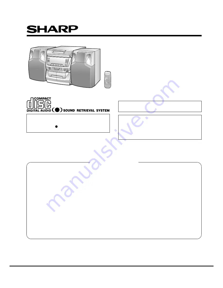
background image

CD-C430H,CP-C430H

– 1 –

 CONTENTS

Page

SAFETY PRECAUTION FOR SERVICE MANUAL ...........................................................................................................  2
IMPORTANT SERVICE NOTES (FOR UK ONLY) ............................................................................................................  3
SPECIFICATIONS .............................................................................................................................................................  3
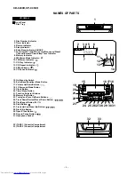
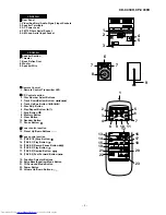
NAMES OF PARTS ...........................................................................................................................................................  4
OPERATION MANUAL ......................................................................................................................................................  6
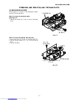
DISASSEMBLY ..................................................................................................................................................................  7
REMOVING AND REINSTALLING THE MAIN PARTS .....................................................................................................  9
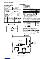
ADJUSTMENT .................................................................................................................................................................. 10
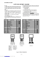
NOTES ON SCHEMATIC DIAGRAM ............................................................................................................................... 12
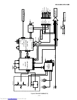
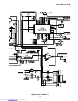
BLOCK DIAGRAM ............................................................................................................................................................ 13
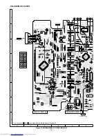
SCHEMATIC DIAGRAM / WIRING SIDE OF P.W.BOARD .............................................................................................. 16
VOLTAGE ........................................................................................................................................................................  29
WAVEFORMS OF CD CIRCUIT ....................................................................................................................................... 30
TROUBLESHOOTING (CD CHANGER CONTROL / CD SECTION) ............................................................................... 31
FUNCTION TABLE OF IC ................................................................................................................................................  35
FL DISPLAY ...................................................................................................................................................................... 41
WIRING OF PRIMARILY SUPPLY LEADS (FOR UK ONLY) .........................................................................................  41
REPLACEMENT PARTS LIST/EXPLODED VIEW
PACKING METHOD (FOR UK ONLY)

SHARP CORPORATION

No. S6739CDC430H/

• In the interests of user-safety the set should be restored to its

original condition and only parts identical to those specified be
used.

CD-C430H and CP-C430H constitute CD-C430H.


• Note for users in UK

Recording and playback of any material may require consent
which SHARP is unable to give. Please refer particularly to the
provisions of Copyright Act 1956, the Dramatic and Musical
Performers Protection Act 1956, the Performers Protection Acts
1963 and 1972 and to any subsequent statutory enactments and
orders.

CD-C430H
CP-C430H

SERVICE MANUAL

• SRS technology Licensed from SRS Labe. SRS technology holds

the follwing patents: U.S. Patent No. 4,748,669, U.S. Patent No.
4,841,572 and U.S. Patent No. 4,866,774.

• SRS the SRS Logo (    ) and the SOUND RETRIEVAL SYSTEM

are registered trademarks of SRS Labs, Inc.

Summary of Contents for CD-C430H

Page 1: ...C430H In the interests of user safety the set should be restored to its original condition and only parts identical to those specified be used CD C430H and CP C430H constitute CD C430H Note for users in UK Recording and playback of any material may require consent which SHARP is unable to give Please refer particularly to the provisions of Copyright Act 1956 the Dramatic and Musical Performers Pro...

Page 2: ...e Except for UK Laser Diode Properties Material GaAIAs Wavelength 780 nm Emission Duration continuous Laser Output max 0 6 mW VARNING OSYNLIG LASERSTRÅNING NÄR DENNA DEL ÄR ÖPPNAD STIRRAEJINISTRÅLENOCHBETRAKTAEJSTRÅLEN MED OPTISKA INSTRUMENT VARO AVATTAESSA OLET ALTTIINA NÄKYMÄTÖN LASERSÄTEILYLLE ÄLÄ TUIJOTA SÄTEESEEN ÄLÄKÄ KATSO SITÄ OPTISEN LAITTEEN LÄPI VARNING OSYNLIG LASERSTRÅLNING NÄR DENNA ...

Page 3: ...7 lbs Amplifier section Output power PMPO 320 W total Except for UK MPO 60 W 30 W 30 W 10 T H D RMS 40 W 20 W 20 W 10 T H D Output power MPO 60 W 30 W 30 W 10 T H D For UK RMS 40 W 40 W 40 W 10 T H D Output terminals Speakers 4 ohms Headphones 16 50 ohms recommended 32 ohms Input terminals Video Auxiliary audio signal 245 mV 47 kohms Tuner section Frequency range FM 87 5 108 MHz AM 522 1 620 kHz C...

Page 4: ...nd by Switch 16 Extra Bass Equalizer Mode Button 17 Volume Up Down Buttons 18 3D Surround Mode Button 19 Clock Button 20 Timer Sleep Button 21 Function Selector Buttons 22 Memory Set Button 23 Tuning and Time Up Down Buttons 24 Track Down Review Preset Down Button 25 Play Repeat Button 26 Stop Button 27 Track Up Cue Preset Up Button 28 Disc Skip Button 29 Open Close Button 30 Record Pause Button 3...

Page 5: ...on 4 Track Up Cue Button 5 Disc Skip Button 6 Play Repeat Button 7 Stop Button 8 Memory Button 9 Clear Button 10 Random Button 11 Pause Button Tuner control section 12 Preset Up Down Buttons Tape control section 13 TAPE 1 2 Stop Button 14 TAPE 1 Play Button 15 TAPE 2 Record Pause Button 16 TAPE 2 Play Button 17 TAPE 2 Rewind Button 18 TAPE 2 Fast Forward Button 19 Function Selector Buttons 20 Extr...

Page 6: ...set to STAND BY 1 Press the MEMORY SET button 2 Perform steps 6 9 above When the ON STAND BY switch is set to ON 1 Press the CLOCK button 2 Within 3 seconds press the MEMORY SET button 3 Perform steps 6 9 above To see the time display When the power is ON Press the CLOCK button The time display will appear for about 3 seconds To switch the time display mode 1 Press the ON STAND BY switch to enter ...

Page 7: ... Socket C3 x4 4 Back Board 1 Screw D1 x5 7 2 5 Main PWB 1 Screw E1 x12 8 1 Display PWB 2 Socket E2 x4 Headphone PWB 6 Front Panel 1 Screw F1 x2 8 1 2 Hook F2 x2 7 Tape Mechanism 1 Open the cassette holder 8 2 2 Screw G1 x6 8 Turntable 1 Screw H1 x1 8 3 2 Cover H2 x1 9 Disc Tray 1 Screw J1 x2 8 3 2 Guide J2 x2 10 CD Changer 1 Screw K1 x4 8 4 Mechanism 11 CD Mechanism 1 Screw L1 x1 8 4 STEP REMOVAL ...

Page 8: ... C430H Figure 8 2 K1 x4 ø3 x12mm L1 x1 ø2 6 x10mm CD Changer Mechanism CD Mechanism Shift Lever CD Player Base Tape Mechanism Open Cassette Holder Power Supply PWB Front Panel G1 x6 ø3 x10mm F1 x2 ø3 x10mm Figure 8 1 E1 x1 ø3 x10mm E1 x1 ø3 x12mm E1 x9 ø3 x10mm E2 x1 E2 x2 E1 x1 ø3 x10mm Front Panel Tape Mechanism E2 x1 Display PWB Main PWB Speaker Box A2 x4 4 x32mm A2 x2 4 x10mm Woofer Figure 8 5...

Page 9: ... to remove the loading motor See Fig 9 1 1 Remove the screws A1 x 2 pcs to remove the loading motor Figure 9 1 A1 x2 ø2 x5mm Loading Motor Figure 9 2 How to remove the pickup See Fig 9 2 1 Remove the screws C1 x 2 pcs to remove the shaft C2 2 Remove the stop washer C3 x 1 pc to remove the gear C4 3 Remove the pickup C1 x2 2 6 x6mm C2 x1 C3 x1 C4 x1 CD Mechanism Pickup ...

Page 10: ... 1 1 0 1 V Tracking 990 kHz 990 kHz T302 1 Test Stage Frequency Frequency Display Setting Adjusting Parts Instrument Connection Setting the Test Mode Keeping the TUNING DOWN button and MEMORY button pressed turn on POWER Then the frequency is initially set in the memory as shown in Table Call it with the PRESET button to use it for adjustment and check of tuner circuit 1 87 50 MHz 6 522 kHz 2 108 ...

Page 11: ...ptimal settings CD SECTION Figure 11 1 Note Only in STOP state it is possible to slide the pickup with the or key VOL Last memory BAL CENTER R GEQ FLAT X BAS OFF Canceling method POWER OFF Setting the test mode Any one of test mode can be set by pressing several keys as follows REC PAUSE DISC SKIP POWER TEST CD operation test TEST mode Function CD test mode Setting of TEST mode Indication of CD TS...

Page 12: ...the capacitor without such a symbol is microfarad As to electrolyticcapacitor theexpression capacitance withstand voltage is used CH TH RH UJ Temperature compensation ML Mylar type P P Polypropylene type Schematic diagram and Wiring Side of P W Board for this model are subject to change for improvement without prior notice REF NO DESCRIPTION POSITION SW1 OPEN CLOSE ON OFF SW2 MECHA UP ON OFF SW3 D...

Page 13: ...QCK COIN SQOUT RWC WRQ CL DAT SELIAL CONTROL CE Q93 Q91 SL SL DRF 7 3 9 8 7 6 5 4 3 2 1 GND D MECHA UP GND D DISK NO OPEN CLOSE GND D M M GND M 9 8 7 6 5 4 3 2 1 CNP10 M 5V 62 64 56 45 36 23 43 37 38 39 40 24 25 10 10 26 58 53 10 12 20 32 40 43 44 53 52 51 54 31 30 29 23 27 16 15 41 44 Q1 5V Q81 5V B5 VOLTAGE REGULATOR VOLTAGE REGULATOR VOLTAGE REGULATOR SWITCHING FROM POWER AMP SECTION TO MAIN SE...

Page 14: ...Q206 Q201 SRS 12V B4 VCC MODE Q124 Q126 SWITCHING BIAS FROM CD SECTION SO401 VIDEO AUX IC201 SRS5250S SRS CIRCUIT 1 3 4 5 1 7 7 8 9 6 20 12 22 15 16 11 21 17 13 10 1 5 4 2 7 3 8 6 8 9 17 14 15 12 10 21 22 23 24 13 18 16 5 4 3 2 6 X352 4 5MHz OSC STEREO ST ST AM IF FM IF IN VT FM IN AM IN FM B4 AM TRACKING AM BAND COVERAGE FE301 FM FRONT END CE DI CL DO T351 IC302 LC72131 PLL FM SWITCHING FM IF CF3...

Page 15: ...AVREF B7 B8 KEY SW701 706 SW709 715 SW717 725 B3 PHM1 RESET Q708 Q709 ZD701 MEMORY BACK UP B7 B8 B7 B8 3 2 1 33 14 21 17 18 30 31 32 Q701 B7 B7 VSS B6 UN SWITCHED FL701 DISPLAY 61 64 POWER VOLTAGE REGULATOR Q971 D971 D973 D961 D964 B2 B1 ZD972 VF2 VP VF1 Q707 Q706 IC701 IX0191AW SYSTEM CONTROL MICROCOMPUTER B3 TO CD SECTION B9 B8 D965 D968 9 43 6 40 49 64 8 44 5 41 7 45 4 42 CD PUIN CD SL CD SL VD...

Page 16: ...121 R102 C117 C123 C113 C111 R107 C107 R101 C102 R108 C108 C101 R110 C1 C1 R60 R58 R3 C3 R3 R2 C1 R1 R701 Q701 C710 C711 FL701 RX701 Q706 D702 R758 C706 Q705 D709 D708 CNP10 C91 R97 IC91 D91 Q91 R95 Q93 C715 R789 R770 R792 R793 R749 C702 R794 L701 D701 Q707 D703 C707 Q708 Q709 ZD701 C709 D704 D706 D705 R763 R777 R836 R835 C855 R764 R133 R172 R768 R736 D5 D7 R49 R82 R61 C43 R778 R88 R87 R783 C44 C1...

Page 17: ...8 C122 C115 C116 R119 R120 Q107 R112 R111 R109 Q108 Q111 Q110 453 C809 C810 C454 R811 C812 C811 C820 C814 R812 R810 809 C813 LG902 C831 C802 C801 C830 C829 C808 C806 C823 C824 C828 Q106 R815 C825 Q104 Q103 Q105 C150 C109 R478 R477 Q109 L104 Q126 C151 C153 Q128 R174 Q124 C152 C218 R160 R476 C422 C452 C420 C418 C406 C405 C412 C402 R420 R419 R418 C401 R416 R415 R403 D2 C37 C35 R475 C39 C40 C2 C404 C3...

Page 18: ...NS102 CNS101 YL WH BK RD WH BK 7 6 5 4 3 2 1 2 1 3 WH BK RD CNP102 P17 8 H TO MAIN PWB P16 6 H TO MAIN PWB CNP101 TAPE MOTOR WH BK MM1 SWM5 SOLM1 SOLENOID CAM BK WH CNP1 CNS1B CNS1A CNS2B CNS2A CNS3B CNS3A BL YL RD WH BK RD WH GY WH GY WH GY WH RD WH GY WH GY WH BL PK RD YL BK CNP2 CNP3 1 2 3 4 5 6 7 8 1 2 3 4 5 6 1 2 3 4 5 1 2 3 4 5 6 7 8 1 2 3 4 5 6 1 2 3 4 5 P17 8 A TO MAIN PWB P17 8 A TO MAIN ...

Page 19: ...305 Q354 Q353 CF351 1 1 2 3 5 10 12 13 15 20 24 BF351 T351 CF302 T302 IC302 CNP303 Q360 R370 2 3 4 5 6 7 8 12 13 14 15 16 17 18 19 20 21 22 L311 C210 C200 R206 C219 R210 R212 C202 R202 R233 R209 R218 R234 G D S 1 B C E 2 3 D201 R208 R207 R215 R216 C223 R217 C224 C240 C220 R200 R203 C203 R204 R205 R228 CNP201 IC201 R201 1 5 10 14 15 20 25 28 R213 Q205 C201 Q201 Q206 R399 TP301 BI901 F962 T2 5A L 25...

Page 20: ...D PD VR LD VREF SP SP_ SL SL_ PU IN SW4 PICKUP IN M1 SPINDLE MOTOR M2 SLED MOTOR PUIN 5V DRF SL SL SQOUT COIN CQCK 5 5 4 4 3 3 2 2 CNS1B 1 CNS1A 1 PD GND LD VR FO_ TR TR_ FO 8 7 6 5 4 3 2 8 7 6 5 4 3 2 CNS2B 1 CNS2A 1 PICKUP UNIT K MON TR FO FO TR LD GND E LD ACTUATOR B C F A LT0H30P1 8 7 6 4 5 3 2 1 4 5 3 2 1 LD VR PD GND F F E F K A B T T A B F K E A B F K E R61 15K 6 5 4 3 2 1 CNP3A R30 15K R26...

Page 21: ...SS EFMO EFMIN TEST2 CLV CLV_ V P HLF TES TA1 MAIN PWB A1 1 3 CD_R GND P26 1 G P23 10 G TO POWER SECTION DISPLAY PWB CD_L M 12V GND D 5V 3 1 MOTOR PWB F M_GND MOTOR GND GND P22 6 G P23 8 G P23 9 G TO DISPLAY PWB D_GND CD_OPEN CLOSE GND DISC_NO UP DOWN CD LD M PUIN NC 4 3V 5V D_GND 12V D_GND GND D MECHA UP GND D DISC NO OPEN CLOSE GND D M M GND M SOL 5V DRF SL RWC WRQ SL RES SQOUT COIN CQCK P24 2 A ...

Page 22: ...RUN FOOL PROOF B T2 RUN GND MOTOR TAPE MECHANIS PWB D MECHA STOP SOLENOIDO T1 RUNPALS T2 RUNPALS B MOTOR GND RUN PALS SENSOR 3 2 P5 P4 P2 P3 3 2 1 1 2W VDD IC REMOCON SYSTEM STOP TUNER SD VDD T0 T1 T2 T3 T4 T5 T6 T7 T8 S0 S1 S2 S3 S4 S5 S6 S7 S8 S9 S10 S11 S12 S13 S14 S15 CD SL CD SL T1 T2 TAPE SOL TAPE MOTOR MIC TAPE F P T1 RUN PLSE TAPE MECHA STOP POWER DISC1 DISC2 DISC3 P B MUTE NC VSS XT2 SL S...

Page 23: ...UT CQCK COIN RWC WRQ BIAS SL SL PUIN DO DI CE CL X1 X2 DI CE CL REC T1_T2 DO RES L_CHECK R_CHECK CNPM2 R709 1K R706 10K R705 10K R703 1K R726 10K D701 1SS119 R766 3 3K R772 100K C715 220 6 3 D705 1SS119 PHM1 MM1 FWM1 FWM2 SWM4 SWM5 SOLM1 SWM3 R734 10K R795 2 2K C709 100 6 3 R786 1K C705 0 01 Q708 KTC3199 GR R776 82 D703 1SS119 R780 10K Q709 KTC3199 GR R785 100 ZD701 MTZJ3 3B Q707 KRC102 M C708 0 0...

Page 24: ...138 6 8K R118 1K C122 1 50 C13 0 06 R134 68K R133 22K C13 22 R14 56 C121 1 50 C13 22 C131 0 001 R1 5 C115 47 10 L107 2 2µH C123 0 015 R123 3 9K C117 0 018 C119 560P R121 100K R119 56 C107 0 001 CNP102 CNP101 R412 22K C414 100P C404 0 047 R403 1K C409 0 047 C405 0 047 C403 0 047 C401 0 047 C413 100P R411 22K C455 220P SO401 C410 0 047 C124 0 015 R120 56 C153 100 16 R174 150 L105 1 5µH C402 0 047 C4...

Page 25: ...2 2 50 C218 2 2 50 C129 470P C132 0 001 R138 6 8K C136 0 068 C140 0 0033 R134 68K C134 22 16 R142 56 C146 220 10 C145 22 16 C147 0 022 C133 22 16 C131 0 001 R141 56 D402 1SS119 D401 1SS119 R478 1K D404 1SS119 D403 1SS119 C438 100P C440 10 16 C433 0 0027 C434 0 0027 C437 100P C445 0 022 C443 22 16 C435 22 16 L104 330µH C135 0 068 R164 4 7K R135 3 3K C148 0 082 R146 10K C128 3 3 25 R153 10K C151 0 0...

Page 26: ...5 10K R807 180 R808 180 C943 470 25 R946 100 R947 270 D941 1SS119 R952 33K ZD951 MTZJ6 2C R951 1 5K C953 0 01 R953 10K C952 47 16 R804 33K R803 33K Q953 KTC3199 GR Q943 KTC3199 GR Q942 2SD2012 Y Q941 2SD2012 Y Q952 2SD2012 Y Q971 KTA1266 R975 220 R976 220 R 3 R973 100 R949 22K R948 22K R945 33K R944 18 R943 18 C974 47 50 C975 47 50 C948 10 50 C947 10 50 C942 100 16 C941 0 022 C945 0 022 C804 560P ...

Page 27: ... voltage 6 5 4 3 2 1 32 31 SPEAKER TERMINAL P23 8 G TO DISPLAY PWB FM SIGNAL SP_R CH SP_R CH_GND SP_L CH_GND SP_L CH ML 1 2W 1 2W 1 2W ML ML ML TO CD GND HEADPHONES HEADPHONES PWB A3 L_CHECK R_CHECK C976 100 35 R974 12K D971 RL104A C972 100 50 C973 47 50 C955 0 22 C956 0 22 C855 560P R811 270 C813 0 1 ML R809 4 7 C811 0 1 ML R836 330 R835 330 JK801 C871 0 001 C872 0 001 SO801 4 7 Q971 KTA1266 GR R...

Page 28: ... 6K R392 390 R318 470 R308 33 C372 1 R391 390 L351 100µH C351 0 022 Q354 KTC3199GR C368 1 Q353 KTC3199GR C399 0 022 R381 10K C391 47 R376 1K R366 10K C394 47 R379 2 2K R380 1 5K R305 6 8K R356 1K C320 0 022 R363 1 8K C322 0 022 ZD351 MTZJ5 1B C325 33P IC303 LA1832 BF351 R304 680 C382 15P C387 0 022 T351 C363 0 022 Q360 KTA1266GR C393 1 IC302 LC72131 C385 0 01 C370 1 CF302 D362 1SS119 R364 1 8K C36...

Page 29: ... 2 6V 0V 0V 0V 0V 0V 4 3V 4 5V 4 4V 4 3V 4V 10 5V 9 8V 4V 0V 4 6V 5 2V 0V 0V 9 8 7 6 5 4 3 2 1 12 11 10 0V 2 5V 4V 0 2V 0V 0V 2 3V 0V 4 3V 5 2V 0 9V 0 9V 0 9V 0 9V 2 4V 1 1V 17 16 15 14 13 20 19 18 0V 0V 2 5V 2 8 V 21 22 PIN NO VOLTAGE IC302 4 8V 5 2V 0V 0V 2 13V 2 14V 4 6V 5V 2 1V 2 1V 2 1V 2 1V 4 5V 4 4V 2 5V 3 5V 4 6V 5 1V 0V 0V 3 4V 2V 3 4V 1 2V 9 8 7 6 5 4 3 2 1 12 11 10 1 3V 1 4V 3 6V 2 2V 2...

Page 30: ... 3 0 5ms 5 0 V HFL 0 5ms 5 0 V TES REVIEW 50ms 10 0 V JP CUE 50ms 10 0 V JP 50ms 0 50 V JP 50ms 1 00 V TE 0 5ms 10 0 V JP 0 5ms 10 0 V JP 0 5ms 0 50 V JP 0 5ms 1 00 V TE REVIEW 50ms 10 0 V JP 50ms 10 0 V JP 50ms 0 50 V JP 50ms 1 00 V TE 0 5ms 10 0 V JP 0 5ms 10 0 V JP 0 5ms 0 50 V JP 0 5ms 1 00 V TE PLAY 20ms 1 00 V SPO NORMAL DISC TN0 01 20ms 2 00 V CLV PLAY TCD 712 140mm TN0 01 50ms 1 00 V SPO 5...

Page 31: ...to stop Is from 5 V till 2 5V down pulse approx 300 ms Check the SWM3 and the wiring from the IC701 pin 21 to the SWM3 No No input into the IC701 pin 21 when the turntable is rotating 5V 2 5V 0V Yes Check IC2 pin26 Q91 and Q93 and the periphery Check the MECHA UP SW and the wiring from the IC701 pin 21 to the MECHA UP SW No Yes Is there following voltage input on the IC701 pin 21 in the specific s...

Page 32: ...ns 24 and 25 IC91 pins 1 and 3 The CD function will not work The CD operating keys don t work Check the CD DSP power supply and 16 93 MHz clock and reset terminal Check the waveform of SCK SO DATA and SI COMM Yes Yes See if the pick up is in the pick up in PICKUP IN SW position If the items mentioned above are OK check the main microcomputer IC701 Yes Yes No Yes No The CD operating keys work Check...

Page 33: ...m Figure 33 2 Figure 33 1 Waveform in case of normal play back HF 1 0V DIV 0 5µsec DIV DC When playing back the disc 3 2 1 4 0 5s 1 00 V IC1 16 FD 0 5s 10 0 V IC2 13 CLV 0 5s 10 0 V IC1 54 DRF 0 5s 2 00 V IC1 7 TE Check the tracking system Check waveform of IC1 pin 7 TE Play is possible in TEST mode Although IL is possible play is impossible Check the periphery of IC 1 pin 14 Normal jump is impede...

Page 34: ...n is performed when disc exits Yes Although HF waveform is normal TOC data cannot be read Yes Check PDO waveform Fig 34 Abnormal Check the IC1 pins 43 and 44 IC2 pins 3 5 7 10 and 11 Stop Play As VCO freque ncy is locked at 4 32 M Hz voltage of PDO rises and stabili zes 2 3 0 5s 1 00 V IC2 3 PDO 0 5s 1 00 V IC2 16 FD Although HF waveform is normal and the time indication is normal no sound is emit...

Page 35: ...VDD Power terminal of digital system 24 CONT1 Input Output General purpose input output terminal 1 25 CONT2 Input Output General purpose input output terminal 2 26 CONT3 Input Output General purpose input output terminal 3 27 CONT4 Input Output General purpose input output terminal 4 28 CONT5 Input Output General purpose input output terminal 5 29 EMPH Output Difference monitor terminal At H deemp...

Page 36: ...Input Input terminal for test Pull down resistor is integrated Surely connected to 0V 63 CS Input Chip selection input terminal Pull down resistor is integrated Connected to 0when not controlled 64 TEST1 Input Input terminal for test Pull down resistor is integrated Surely connected to 0V Pin No Note The same potential must be supplied to the power terminals VDD VVDD LVDD RVDD XVDD In this unit th...

Page 37: ...pindle amplifier input 25 SPG Pin to connect gain setting resistor in the 12cm mode of spindle 26 SP Pin to connect spindle phase compensation constant together with SPD pin 27 SPD Spindle control signal output pin 28 SLEQ Pin to connect thread phase compensation constant 29 SLD Thread control signal output pin 30 SL Input pin of thread feed signal from micro computer 31 SL Input pin of thread fee...

Page 38: ...PH1 Pin to connect capacitor for peak hold of RF signal 61 BH1 Pin to connect capacitor for bottom hold of RF signal 62 LDD APC circuit output pin 63 LDS APC circuit output pin 64 VCC1 RF system VCC pin Figure 38 BLOCK DIAGRAM OF IC 1 FIN2 FIN1 E F TB TE TE TESI SCI TH TA TD TD JP TO FD FD FA FA FE FE AGND SP SPI SPG SP SPD SLEQ SLD SL SL JP JP TGL TOFF TES HFL SLOF CV CV RFSM RFS SLC SLI DGND FSC...

Page 39: ...t with UNBACK UP VDD 31 P04 SRS Input SRS provided not provided 32 XT2 Non connect 33 VSS Connect with GND 34 X1 X1 Input MAIN CLOCK 4 19MHz 35 X2 X2 Output MAIN CLOCK 4 19NHz 36 P37 C2 B CL Output C2 B Bus clock 37 P36 C2 B CE Output C2 B Bus chip enable 38 P35 C2 B DI Output C2 B Bus comand 39 P34 C2 B DO Input C2 B Bus data 40 P33 CD DRF Input Data read fiug from DSP 41 P32 CD PUIN Input L Inne...

Page 40: ...C CD DSP CQCK CD DSP COIN CD DSP SQOUT RESET INPUT CD DSP RES CD T T OPEN CLOSE CONNECT WITH GND CD UP DOWN DISC NO T2 RUN PLSE Lch INPUT Rch INPUT 25 26 27 28 29 30 31 32 33 34 35 36 37 38 39 40 80 79 78 77 76 75 74 73 72 71 70 69 68 67 66 65 64 63 62 61 60 59 58 57 56 55 54 53 52 51 50 49 48 47 46 45 44 43 42 41 FIP22 FIP23 FIP24 FIP25 P120 P121 P122 P123 P124 P125 P126 P127 VDD P70 P71 P72 IC I...

Page 41: ...sformer Nylon Band 80mm 92LN BAND 1318A AC Power Supply Cord Brown Blue Core IC5 VHiM5674FP 1 Focus Tracking Spin Slide Driver M5674FP Figure 41 1 BLOCK DIAGRAM OF IC OP1 15K 15K 25K 23K TSD 1 19 20 21 22 23 24 25 26 27 28 29 30 31 32 33 34 35 36 Regbase Vcc Vctl3 Vctl3 Vctl3 out VM3 VM3 GND VM4 VM4 Vctl4 Gain4 Standby SS GND Standby 2 3 4 5 6 7 8 9 10 11 12 13 14 15 16 17 18 Vrel in Vrel out N C ...

Page 42: ...CD C430H CP C430H 42 M E M O ...

Page 43: ...wire VC TQ Square type without lead wire VC CY Square type without lead wire VC CZ Square type without lead wire VC J The 13th character represents capacity difference J 5 K 10 M 20 N 30 C 0 25 pF D 0 5 pF Z 80 20 If there are no indications for the electrolytic capacitors error is 20 Resistors VRD Carbon film type VRS Carbon film type VRN Metal film type VR MF Cylindrical type without lead wire V...

Page 44: ...ener 5 1V MTZJ5 1B ZD352 VHEMTZJ3R9B 1 J AC Zener 3 9V MTZJ3 9B ZD701 VHEMTZJ3R3B 1 J AA Zener 3 3V MTZJ3 3B ZD941 VHEMTZJ130A 1 J AC Zener 13V MTZJ13A ZD951 VHEMTZJ6R2C 1 J AC Zener 6 2V MTZJ6 2C ZD971 VHEMTZJ300B 1 J AB Zener 3V MTZJ3B ZD972 VHEMTZJ6R2A 1 J AA Zener 6 2V MTZJ6 2A FILTERS BF351 RFILA0009AWZZ J AE AM IF CF301 302 RFILF0072AFZZ J AG FM IF CF351 RFILF0003AWZZ J AK FM IF TRANSFORMERS...

Page 45: ...µF 50V Electrolytic C394 RC GZA476AF1C J AB 47 µF 16V Electrolytic C395 VCTYMN1EF223Z J AA 0 022 µF 25V C396 RC GZA107AF1A J AB 100 µF 10V Electrolytic C397 VCKYMN1HB221K J AA 220 pF 50V C398 RC GZA107AF0J J AB 100 µF 6 3V Electrolytic C399 VCTYMN1EF223Z J AA 0 022 µF 25V C401 406 RC QZA473AFYK J AB 0 047 µF 50V Mylar C407 408 VCKYMN1HB391K J AA 390 pF 50V C409 410 RC QZA473AFYK J AB 0 047 µF 50V ...

Page 46: ...W R150 VRD MN2BD103J J AA 10 kohm 1 8W R152 VRD MN2BD102J J AA 1 kohm 1 8W R153 154 VRD MN2BD103J J AA 10 kohm 1 8W R158 VRD ST2EE471J J AA 470 ohms 1 4W R160 VRD RT2HD151J J AA 150 ohms 1 2W R162 VRD MN2BD472J J AA 4 7 kohms 1 8W R164 VRD MN2BD472J J AA 4 7 kohms 1 8W R166 VRD MN2BD473J J AA 47 kohms 1 8W R167 VRD MN2BD104J J AA 100 kohm 1 8W R168 VRD MN2BD120J J AA 12 ohms 1 8W R172 VRD ST2CD102...

Page 47: ...Plug 8Pin CNP3 92LCONE6P53253 J AC Plug 6Pin CNP3A 92LCONE6P53254 J AC Plug 6Pin CNP10 92LCONEAP53254 J AD Plug 10Pin CNP101 QCNCM742CAFZZ J AA Plug 3Pin CNP102 QCNCM588GAFZZ J AB Plug 7Pin CNP201 QCNCW010FAWZZ J AE Socket 6Pin CNP301 QCNCM602BAFZZ J AA Plug 2Pin CNP303 QCNCW010KAWZZ J AD Socket 10Pin CNP401 QCNCM010FAWZZ J AD Plug 6Pin CNP402 QCNCM010KAWZZ J AC Plug 10Pin CNP901 QCNCM742FAFZZ J A...

Page 48: ... CABINET PARTS 201 92LCAB2547AS1 J AX Front Panel Ass y 201 1 Front Panel Not Replacement Item 201 2 PCUSG0022AWZZ J AB Cushion Leg 201 3 HDECQ0224AWSA J AK Panel Amp 202 GCAB 1045AWSB J AL Top Cabinet 5 203 GITAR0219AWSA J AG Back Board Except for UK Thailand 203 GITAR0220AWSA J AG Back Board For UK 203 GITAR0222AWSA J AG Back Board For Thailand 204 92LMEC2475CTS1 J AL Cassette Holder Ass y Tape ...

Page 49: ...QANTL0005AWZZ J AG AM Loop Antenna 7 92LF ANT1535A J AF FM Antenna 8 92LCARD1751A J AB Registration Card For UK Only 9 RRMCG0100AWSA J AR Remote Control 9 1 92LLiD1782A J AQ Battery Lid Remote Control 10 SPAKZ0265AWZZ J AB Mira Mat 11 92LBAG1770A J AB Polyethylene Bag AC Power Supply Cord 12 SPAKZ0264AWZZ J Sheet P W B ASSEMBLY Not Replacement Item PWB A1 3 92LPWB2546MANS J Main Display Headphones...

Page 50: ...CD C430H CP C430H 50 A B C D E F G H 1 2 3 4 5 6 Figure 7 CD MECHANISM EXPLODED VIEW 7 306 1 701 304 701 302 301 702 702 303 M1 703 305x2 SW4 M2 305 PWB E 306 2 306 3 306 704 CD C430H ...

Page 51: ...4 3 7 7 38 18 4 506 33 55 17 22 2 37 38 27 20 42 19 21 26 20 13 35 502 30 507 SOLM1 28 1 52 53 506 9 502x2 501x2 503x2 503x2 503x3 44 10 16 11 29 43 45 503 505 13 SWM5 MM1 PWB D 14 32 15 504 41 TAPE1 TAPE2 502 5 39 55 36 36 503x3 40 SWM3 SWM4 31 31 12 12 57 58 57 58 509 503 510 508 45 43 44 10 9 8 MOTOR BELT CONNECTION CD C430H ...

Page 52: ...WB A1 263 FL701 209 1 209 2 201 3 201 1 201 223 224 221 222 603 213 603 213 226 225 204 1 204 2 206 1 206 2 214 208 215 201 2 201 2 606x2 620x4 216 210 210 2 210 1 619 623 601x6 220 618x2 618 260x2 252 602 253 203 253 618 625x2 623x3 623x3 623x2 619x8 206 204 618x2 618 261 619 255 264x2 260x4 217 80 mm PWB A2 PWB A3 PWB B a b PWB C b 253 605 254 ...

Page 53: ...EW 2 2 10 CD C430H 603 243 250 240 241 242 243 603 250 612x4 243 257 228 270 M3 PWB F 621x2 SW2 227 233 234 235 236 229 229 237 622 610 238 239 610 232 231 230 243x2 243 243 243 SW3 246 602 614 247 248 1 249 608x2 608x2 202 211 266 CD MECHANISM 248 2 248 3 248 267 256 613 245 244 ...

Page 54: ...LODED VIEW A B C D E F G H 1 2 3 4 5 6 CP C430H 11 SHARP SP1 2 TWEETER C1 2 2 7µF 100V N P C1 2 2 7µF 100V N P SP1 2 TWEETER SP3 4 WOOFER SP3 4 WOOFER 702 705 701 703 707 706 710 SP3 4 709x2 709x2 704x2 708x2 708x2 SP1 2 BLACK BLACK RED RED RED ...

Page 55: ...n Manual TiNSE0162AWZZ 6 AM Loop Antenna QANTL0005AWZZ 7 FM Antenna 92LF ANT1535A 8 Registration Card 92LCARD1751A 9 Remote Control RRMCG0100AWSA 10 Mira Mat SPAKZ0265AWZZ 11 Polyethylene Bag AC Power Supply Cord 92LBAG1770A 12 Sheet SPAKZ0264AWZZ CP C430H 1 Polyathylene Bag Speaker 92L411 0075 2 Mirror Mat 92L4140011 3 Packing Add Speaker Top Bottom 92L412 0077 4 Center Pad 92L416 0030 5 Feature ...

Page 56: ...CD C430H CP C430H 56 Writer and Editor Quality Reliability Control Center of Audio Visual Systems Group Sharp Corp A9706 4728NS HA M Printed in U K SG SK STCL ...

Reviews: