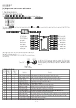
background image

1 - 1

UX-470ES/SE/AT

FO-880ES/AT

Illustration: UX-470

No. 00ZUX470ESSME

CHAPTER 1. GENERAL DESCRIPTION
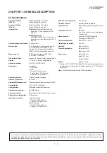
[1] Specifications ............................................ 1-1
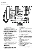
[2] Operation panel ......................................... 1-2
[3] Refer to the service manual of UX-370ES.
[4] Refer to the service manual of UX-370ES.
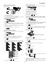
[5] Quick reference guide ............................... 1-9
[6] Refer to the service manual of UX-370ES.

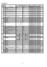
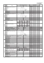
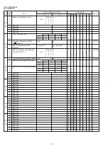
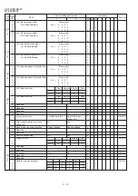
CHAPTER 2. ADJUSTMENTS
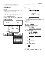
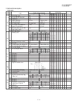
[1] Adjustments .............................................. 2-1
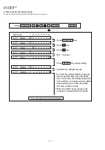
[2] Diagnostics and service soft switch .......... 2-2
[3] Troubleshooting ......................................  2-17
[4] Error code table ....................................... 2-18

CHAPTER 3. MECHANISM BLOCKS
[1] Refer to the service manual of UX-370ES.
[2] Refer to the service manual of UX-370ES.

CHAPTER 4. DIAGRAMS
[1] Block diagram ............................................ 4-1
[2] Wiring diagram .......................................... 4-2
[3] Point-to-point diagram ............................... 4-3

CHAPTER 5. CIRCUIT DESCRIPTION
[1] Circuit description ..................................... 5-1
[2] Circuit description of control PWB ............ 5-2
[3] Circuit description of TEL/LIU PWB .......... 5-8
[4] Circuit description of
            power supply PWB ............................ 5-11
[5] Circuit description of CIS unit ................... 5-11

CHAPTER 6. CIRCUIT SCHEMATICS AND
PARTS LAYOUT
[1] Control PWB circuit ................................... 6-1
[2] TEL/LIU PWB circuit .................................. 6-9
[3] Power supply PWB circuit ......................  6-17
[4] Operation panel PWB circuit ................... 6-19

CHAPTER 7. OPERATION FLOWCHART
[1] Refer to the service manual of UX-370ES.
[2] Refer to the service manual of UX-370ES.

CHAPTER 8. OTHERS
[1] Refer to the service manual of UX-370ES.
[2] Refer to the service manual of UX-370ES.
PARTS GUIDE

CONTENTS

FACSIMILE

UX-470

MODEL 

FO-880

Parts marked with "

" is important for maintaining the safety of the set. Be sure to replace these parts with specified ones for

maintaining the safety and performance of the set.

This document has been published to be used
for after sales service only.
The contents are subject to change without notice.

SHARP CORPORATION

SERVICE MANUAL

This service manual is omitted because it is partly common to UX-370ES/SE/F/FO-780AT/ES of the service manual
of the previous issue. Those common parts are to refer to the service manual of UX-370ES/SE/F/FO-780AT/ES
(00ZUX370ESSME).

SELECTION CODE

COUNTRY

UX-470ES/FO-880ES

Spain

UX-470SE

Sweden

UX-470AT/FO-880AT

Austria

Summary of Contents for FO-880

Page 1: ...UIT SCHEMATICS AND PARTS LAYOUT 1 Control PWB circuit 6 1 2 TEL LIU PWB circuit 6 9 3 Power supply PWB circuit 6 17 4 Operation panel PWB circuit 6 19 CHAPTER 7 OPERATION FLOWCHART 1 Refer to the service manual of UX 370ES 2 Refer to the service manual of UX 370ES CHAPTER 8 OTHERS 1 Refer to the service manual of UX 370ES 2 Refer to the service manual of UX 370ES PARTS GUIDE CONTENTS FACSIMILE UX ...

Page 2: ...almistajan ohjeiden mukaisesti French ATTENTION Il y a danger d explosion s il y a remplacement incorrect de la batterie Remplacer uniquement avec une batterie du même type ou d un type recommandé par le constructeur Mettre au rébut les batteries usagées conformément aux instructions du fabricant Swedish VARNING Explosionsfare vid felaktigt batteribyte Använd samma batterityp eller en ekvivalent t...

Page 3: ...e Configuration Half duplex desktop transceiver Compression scheme MH MR Sharp Scanning method Sheet feeder CIS Contact Image Sensor Effective recording width 204 mm max Input document size Automatic feeding Width 148 to 210 mm Length 140 to 297 mm Manual feeding Width 148 to 210 mm Length 140 to 600 mm Effective scanning width 210 mm max Contrast control Automatic Dark selectable Copy function Si...

Page 4: ...olume of the ringer at all other times 9 FUNCTION key FUNKTION Tecla FUNCION Press this key to select various special function 10 Panel release BEDIENFELD ENTRIEGELN Liberación del panel Grasp this finger hold and pull toward you to open the operation panel 11 Number keys Zifferntasten Teclas numéricas Use these keys to dial numbers and enter numbers and letters during number name storing procedur...

Page 5: ... A B C D E F G H I J K L M N O P Q R S T U V W X Y Z SPACE SPEED DIAL REDIAL SEARCH SPEAKER ABC DEF JKL MNO GHI TUV WXYZ PQRS SYMBOLS R Deletes high lighted letter Upper lower case shift key Moves cursor to the left Moves cursor to the right Press either key one or more times to select and enter a symbol START MEMORY STOP FUNCTION ES SE 3 FUNCTION AT 3 SPEAKER FUNCTION 3 SPEED DIAL FAX TEL A M FAX...

Page 6: ...1 4 UX 470ES SE AT FO 880ES AT M E M O 1 11 ...

Page 7: ... MG 3 24V 4 24V 5 24V 6 DG 7 5V 8 DG 9 PSAVE Connector No CNPW Pin No 2 1 TEL LIU PWB POWER SUPPLY PWB CONTROL PWB CNLIUA CNLIUA CN1 CNPW CNTH CNPN CNCIS CNSP CNMT CNCSW CNLIUB CNLIUB 2 IC protectors replacement ICPs IC Protectors are installed to protect the motor driver circuit ICPs protect various ICs and electronic circuits from an overcurrent con dition The location of ICPs are shown below CO...

Page 8: ...eck Flash memory clear START START START KEY STOP KEY Power ON Memory clear Work Backup FLN0 All black mode START FMH0 START 7 Memory clear Shading mode START 8 FMM0 FLP0 FMI0 2 Diagnostic items ITEM DIRECT DIRECT No key key Contents Function UX 470 FO 880 1 1 1 SOFT SWITCH MODE Soft switches are displayed and changed List can be output 2 2 2 ROM RAM CHECK ROM is sum checked and RAM is matched Res...

Page 9: ...Signal send mode This mode is used to send various signals to the circuit during FAX com munication Every push of START key sends a signal in the following sequence Moreover the signal sound is also output to the speaker when the line monitor of the soft switch is on 1 No signal CML signal turned on 2 9600bps 3 7200bps 4 4800bps 5 2400bps 6 300bps FLAG 7 2100Hz CED 8 1100Hz CNG 9 END 3 7 Memory cl...

Page 10: ... T SW A1 1 0 0 0 0 0 0 0 S F T SW A1 1 0 0 0 0 0 0 0 S F T SW A2 0 0 0 0 0 0 0 0 S F T SW M2 0 0 0 0 0 0 0 0 Press key during setting To finish the settings halfway between SW A1 and SW M2 press the STOP key In this case the setting being done to the SW No on display will be nullified while settings done to the preceding SW Nos remain in effect The soft switch mode is terminated S F T SW A1 0 0 0 ...

Page 11: ...r 8 CNG transmission No Yes 0 0 0 CED tone signal interval 1000ms 750ms 500ms 75ms 1 No 1 1 1 0 0 0 0 0 2 No 2 1 0 1 0 0 0 0 3 MR coding No Yes 0 0 0 4 Reserved 0 0 0 5 Reserved 0 0 0 6 Reserved 0 0 0 7 Reserved 0 0 0 8 Reserved 0 0 0 1 Signal transmission level Binary input 0 0 0 2 No 16 8 4 2 1 1 1 1 3 1 2 3 4 5 0 1 1 4 0 1 0 1 1 ES 1 0 0 5 0 1 1 0 0 SE AT 1 0 0 6 Protocol monitor error print Pr...

Page 12: ... 1 1 2 Dial tone detection before auto dial No Yes 0 0 0 3 Reserved 0 0 0 4 Busy tone detection after auto dial No Yes 0 0 0 5 Waiting time after dialing 90 sec 45 sec 0 0 0 6 Reserved 0 0 0 7 Reserved 0 0 0 8 PBX connection Yes No 0 0 0 OPTION PBX recall function R key select No Earth Flash OPTION 1 No 1 0 1 1 1 1 1 2 No 2 0 0 1 1 1 1 3 Reserved 0 0 0 PBX select ID Earth Flash OPTION 4 No 4 0 1 1...

Page 13: ...to receive Binary input OPTION 1 No 8 4 2 1 0 0 0 2 1 2 3 4 0 0 0 3 0 0 1 0 ES 1 0 0 4 0 0 0 1 SE AT 0 1 1 5 Automatic switching manual to auto Reception after 5 No reception 0 0 0 receive mode rings 6 Reserved 0 0 0 7 CI detection 13 Hz or more As is PTT 0 0 0 8 Reserved 0 0 0 1 Reserved 0 0 0 2 Reserved 0 0 0 3 Reserved 0 0 0 4 Reserved 0 0 0 5 Caller ID function SE only Yes No 0 0 0 OPTION SE o...

Page 14: ...N Number of CNG detect AM mode 1pulse 2pulses 3pulses 4pulses 2 No 2 0 0 1 1 0 0 0 3 No 3 0 1 0 1 1 1 1 Number of CNG STAND BY mode 1pulse 2pulses 3pulses 4pulses 4 No 4 0 0 1 1 0 0 0 5 No 5 0 1 0 1 1 1 1 6 Reserved 0 0 0 7 Reserved 0 0 0 8 Reserved 0 0 0 1 Reserved 0 0 0 2 Reserved 0 0 0 3 Reserved 0 0 0 4 Reserved 0 0 0 5 Reserved 0 0 0 6 Reserved 0 0 0 7 Reserved 0 0 0 8 Reserved 0 0 0 1 Reserv...

Page 15: ...Yes No 0 0 0 OPTION 8 Reserved 0 0 0 ICM recording time 4min 15s 30s 60s OPTION 1 No 1 0 0 1 1 0 0 1 2 No 2 0 1 0 1 0 0 1 A M quiet time 1 2s 3s 4s 5s 3 No 3 0 0 1 1 0 0 0 4 No 4 0 1 0 1 0 0 0 A M quiet time 2 0s 1s 2s 3s 5 No 5 0 0 1 1 1 1 1 6 No 6 0 1 0 1 0 0 0 7 Key input buzzer on off switch On Off 0 0 0 Two way recording mode 8 Reserved 0 0 0 1 A M quiet detect time Binary input 0 0 0 2 No 16...

Page 16: ...t Fast 1 No 1 0 0 1 1 0 0 0 2 No 2 0 1 0 1 1 1 1 AGC slew rate Mic Slow Normal Little fast Fast 3 No 3 0 0 1 1 0 0 0 4 No 4 0 1 0 1 1 1 1 5 Reserved 0 0 0 6 Reserved 0 0 0 7 Reserved 0 0 0 8 Reserved 0 0 0 1 Activity report print Automatic printout No printout when 0 0 0 OPTION memory full 2 Total communication hours and No Yes 0 0 0 pages print 3 Sender s phone number setting Cannot change Change...

Page 17: ...TION 6 A4 paper enable Enable Disable 1 1 1 7 LEGAL LETTER paper enable Enable Disable 0 0 0 8 2 IN 1 mode Yes No 0 0 0 OPTION Paper set size LETTER LEGAL A4 1 No 1 0 0 1 1 1 1 2 No 2 0 1 0 0 0 0 3 Automatic reduce of receive Auto 100 1 1 1 OPTION 4 Print contrast Light Normal 0 0 0 OPTION 5 Reception reduction ratio in case of 100 93 0 0 0 OPTION memory full 6 Reserved 0 0 0 7 Reserved 0 0 0 8 Re...

Page 18: ...de list at the front end of receiver s original when original is sent to the remote machine If this switch is set to NO the HEADER PRINT is not output at the receiving machine SW A2 No 6 H2 mode Used to determine reception of H2 mode 15 sec transmission mode When set to OFF H2 mode reception is inhibited even though the transmitting machine has H2 mode function SW A2 No 7 Communication error treat...

Page 19: ...ls after dialing SW B2 No 6 No 7 Reserved Set to 0 SW B2 No 8 PBX connection Used to select according to the connected line PBX Private Branch Exchange SW B3 No 1 No 2 PBX recall function R key select Used to set the operation mode of PBX recall when the R key is pressed Setting is made according to the type of PBX No 1 1 No 2 1 Time break recall Flash is performed No 1 1 No 2 0 Earth recall is pe...

Page 20: ...my ringer on TEL FAX automatic switching mode SW E1 No 4 Number of CNG signal detection at the tel fax auto matic switching mode Used for detection of CNG in one tone or two tones in the TEL FAX automatic switching mode SW E1 No 5 No 6 Reserved Set to 0 SW E1 No 7 Post answer tone transmit in Tel Fax mode When set to 0 machine send the 800 Hz tones in TEL FAX auto changeover mode SW E1 No 8 Reserv...

Page 21: ...ages with average energy below the AGC Energy Reference Level will have their average energy level increased by no more than the AGC Maxi mum Gain The AGC Maximum Gain should average energy of the mes sage with the lowest average energy to the AGC Energy Reference Level SW I4 No 5 No 8 AGC maximum gain Mic 10 25dB 1dB step The AGC Maximum Gain limits the gain applied by the AGC Messages with avera...

Page 22: ...lume from a speaker SW J3 No 1 Automatic cover sheet The machine automatically generates a cover sheet and sends it as the last page of each transmission SW J3 No 2 No 4 Communication result printout Transaction report Every communication the result can be output As usual it is set to print the timer sending communication error alone If No 2 0 No 3 1 No 4 0 are set printing is always on printed ev...

Page 23: ...use the following format and check the related matters TO ATT Ref No CC ATT Date FM Dept Sign Please complete this report before calling the TAC hotline if problem still occurs Facsimile communication problem Ref No Date From Mr Fax Tel No Our customer Name Tel No Address Fax No Contact person Model name Other party Name Tel No Address Fax No Contact person Model name Problem mode Line Domestic in...

Page 24: ...Error occurred just after fallback 13 Error occurred after a response to retransmission end command was received G3 Reception Code Final received signal Error Condition Receiver side 0 Incomplete signal frame Cannot recognize bit stream after flag 1 NSS DCS Cannot recognize CFR or FTT signal Disconnects line during transmission line error 2 NSC DTC Cannot recognize NSS signal FIF code etc 3 EOP Ca...

Page 25: ...UX 470ES SE AT FO 880ES AT 2 19 M E M O ...

Page 26: ...GINE FC100 M HANDSET SPEAKER 5V 24V OPERATION PANEL TEL LIU PWB UNIT DRIVER THERMAL HEAD PM CONTACT IMAGE SENSOR DOCUMENT SENSOR POWER SUPPLY PWB UNIT REGULATOR SELECT SPEAKER AMPLIFIER AMPLIFIER AMPLIFIER SURGE PROTECT FILTER CML TRANSFORMER CI VBT STABILIZER RECTIFIER TRANSFORMER RECTIFIER DIODE TRANS SURGE ABSORBER FILTER LINE EXT TEL P IN SENSOR RESET IC AMPLIFIER BZ CLOCK 19 66MHz BLOCK AMPLI...

Page 27: ...AGE SENSOR LCD UNIT CNLCD OPERATION PANEL PWB NUIT 14 CNPN 16 7 15 CNCSW CNMT CNTH CNCIS CNPN CNSP SPEAKER CNLIUA CNPW 9 CONTROL PWB UNIT TEL LIU PWB UNIT POWER SUPPLY PWB UNIT CNLIUA CN1 EXTERNAL LINE TEL LINE MJ1 2 MJTEL AC CORD TX RX MOTOR 2 HANDSET FG FG FG ARG 6 CNLIUB CNLIUB 14 ...

Page 28: ...HIT CISCLK GLED 24V KEN4A KEN3A KEN2A KEN1A DG DG 5V ORGSNS FRSNS E SEN4 SEN0 SEN1 SEN2 SEN3 KEN4A KEN3A KEN2A KEN1A DG DG 5V ORGSNS FRSNS E SEN4 SEN0 SEN1 SEN2 SEN3 CNPN CNPN CNCIS 1 2 3 4 5 6 7 8 9 10 11 12 13 14 1 2 3 4 5 6 7 8 9 10 11 12 13 14 TEL LIU PWB TELOUT TELIN TELMUTE CI HS P E P IN RHS RXIN TXOUT CML 5V DG 24VA TELOUT TELIN TELMUTE CI HS PE PIN RHS RXIN TXOUT CML 5V DG 24V CNLIUA CNLI...

Page 29: ...n the transmit buffer of the RAM The data is then converted from parallel to serial form by the modem where the serial data is modulated and sent onto the line Receive operation There are two ways of starting reception manual and automatic Depression of the START key in the off hook mode in the case of manual receive mode or CI signal detection by the LIU in the auto matic receive mode First the F...

Page 30: ...DMA CONTROLLER OPERATOR PANEL IF 32 KEYS 8 LEDS LCD MODULE MOTOR POWER CONTROL RINGER SYNC SERIF 1 THERMAL PRINTER IF 5 ms LINE TIME A4 B4 LINES TPH ADC 4 STROBE TPH LATCHLESS TPH EXTEMAL DMA I F T 4 T 6 CODEC MH MR MMR HARDWARE ALTERNATE COMPRESSION DECOMPRESSION BI LEVEL RESOLUTION CONVERSION PROGRAMMABLE REDUCTION EXPANSION 2 6kBYTE VIDEO RAM SCANNER CONTROL VIDEO PROCESSING 8 BIT PADC CCD CIS ...

Page 31: ...owered by battery power but the output drive is powered by DRAM battery power Scanner Interface START 101 O 2XS Scanner shift gate control CLK1 100 O 2XS Scanner clock CLK1n 99 O 2XS Scanner clock inverted CLK2 98 O 2XS Scanner reset gate control or clock for CIS scanner FCS1n VIDCTL0 96 O 2XT Flash memory chip select or Video Control signal FCS2n VIDCTL1 97 O 2XT Flash memory chip select or Video...

Page 32: ... 3 n 79 I O H 2XC Hysteresis In GPIO 13 or I O chip select 3 GPIO 14 CS 4 n 78 I O H 2XC Hysteresis In GPIO 14 or I O chip select 4 GPIO 15 CS 5 n 77 I O H 2XC Hysteresis In GPIO 15 or I O chip select 5 GPIO 16 IRQ 8 76 I O H 1XC Hysteresis In GPIO 16 or external interrupt 8 GPIO 17 IRQ 5 n 75 I O H 1XC Hysteresis In GPIO 17 or external interrupt 5 GPIO 18 IRQ 9 n 74 I O H 1XC Hysteresis In GPIO 1...

Page 33: ...NSORS START CLK2 CLK1 CLK1N VIDCTL 1 0 XIN XOUT MIRON MCSN SYSCLK D 7 0 RDN A 4 0 WRN MONOFAX FACSIMILE MODEM ANALOG SWITCH LINE INTERFACE SPEAKER MICROPHONE CIRCUIT TELEPHONE LINE RXA TXA SPKR MIC RIN SPKRLO SPKRHI SPKR RIN TXA2 TXA1 TXOUT RXIN XIA GPIO DRAM OPTION SCANNER VIDEO PREPROCESSING SYNC PORTS 2 SSIF VIN VREF VREF SSCLK 2 1 SSTXD 2 1 SSRXD 2 1 SSSTAT 2 1 SYNC ASYNC SERIAL PORT SASCLK SA...

Page 34: ...ciently store and playback digital incoming mes sages ICMs and outgoing messages OGMs The ADPCM audio codec compresses audio signals e g music voice at 32 kbps or 24 kbps for highest fidelity coding and reproduction Selectable error correction coding allows storage in audio grade RAMs ARAMs Echo cancellation techniques employed during playback al low DTMF and tone detection during voice audio code...

Page 35: ...IN MI 49 NC 50 IACLK MI 51 NC 52 CS IA 53 READ IA 54 GPI2 IA 55 GPI3 IA 56 GPI4 IA 57 GPI5 IA 58 VDD2 PWR 59 GPI6 IA Pin No Signal Name I O Type 60 GP17 RINGD IA 61 GPO7 OB 62 GPO6 OB 63 GPO5 OB 64 GPO4 OB 65 GPO3 OB 66 DGND2 GND 67 CTS OA 68 IRQ1 OC 69 GPO2 OB 70 GPO1 OB 71 GPO0 OB 72 RESET OA 73 XTLI I 74 XTLO O 75 XCLK OD 76 YCLK OD 77 VDD3 PWR 78 IRQ2 OC 79 SR3IN MI 80 DGND3 GND 81 DGND4 GND 8...

Page 36: ...T VOL A VOL C TXMUTE DPMUTE RCVOL2 RCVOL RXIN E RLY RCVOL DG SPEAKER L H BZOUT TXCONT GAINC SIGMUTE VOL A VOL B L H MONITOR 3 Circuit description of TEL LIU PWB 1 TEL LIU block operational description 1 Block diagram 2 Circuit description The TEL LIU PWB is composed of the following 10 blocks 1 Surge protection circuit 2 Noise filter 3 Dial pulse generation circuit 4 CML relay 5 Matching transform...

Page 37: ...through the ES C3 0 47µF R3 51K SE C3 0 56µF R3 22K AT C3 1 0µF R3 15K and ZD2 when the ring signal is inputted from the telephone line 10 Power supply and bias circuits The voltages of 5V and 24VA are supplied from the control PWB unit Signal Name Description CML Line connecting relay and DP generating relay The circuit is located H Line make in the TEL LIU PWB L Line break Speaker tone mute cont...

Page 38: ...sion DTMF analog signal output from modem RXIN Reception DTMF others analog signal input into modem Other signals NO Signal Name CNLIUA 8 RHS 9 RXIN 10 TXOUT 11 CML 12 5V 13 DG 14 24VA NO Signal Name CNLIUB 1 N C 2 RLYCNT 3 SIGMUTE NO Signal Name CNLIUB 4 DPON 5 DPMUTE 6 E RLY H L H L CML CI DETECT LINE EXT HI GAIN TXOUT TXMUTE L H MODEM R96V24 CONTROL PWB TEL LIU PWB TEL TEL H L EARTH H L HS AGC ...

Page 39: ...sor which puts the original paper in close contact with the full size sensor for scanning being a monochromatic type with the pixel number of 1 728 dots and the main scanning density of 8 dots mm It is composed of sensor rod lens LED light source light conductive plate control circuit and so on and the reading line and focus are previously adjusted as the unit Due to the full size sensor the focus...

Page 40: ... A0 RD WR ROMCS CS1 MCS SYNC REGDMA WAIT RAS CAS0 CAS1 DWR WRPROT A16 A15 A14 A13 A12 A11 A10 A9 A8 A7 A6 A5 A4 A3 A2 A1 A0 32 C182 0 1 5V RA5 270x4 90 GPIO4 100 CLK1 30 PDAT 24 A3 57 CS0 GPIO3 GPIO2 GPIO1 GPIO0 CNPW 9 PSAVE CNLIUA 11 100Px4 CNLIUA 8 RHS CNLIUA 5 HS CI TELMUTE R206 470 R204 470 R180 30K STRB3 CNTH 4 STRB2 CNTH 3 PCLK DATA CNTH 14 CNTH 15 CNTH 13 LATCH R153 470 R169 150 RA12 100x4 ...

Page 41: ...114 0 1 FRD 1 4A FCS 1 3A FREADY 1 4A CE1 A16 21 A15 20 A14 29 19 A13 28 18 A12 17 A11 25 15 A10 23 14 A9 26 13 A8 27 A7 A6 31 A5 32 A4 1 A3 A2 10 A1 11 16 A0 12 5V C127 0 1 D7 D6 D5 D4 D3 D2 D1 D0 IC4 27C020 2 A16 D7 3 A15 D6 A14 D5 A13 D4 4 A12 D3 A11 D2 A10 D1 A9 D0 A8 5 A7 6 A6 VCC 7 A5 PGM 8 A4 VPP 9 A3 A2 A1 GND A0 A17 30 A17 DG DG C126 N M CE OE 22 24 ROMCS 1 3I DG 12 CE2 2 2I CS1 VBT R117 ...

Page 42: ...0 5P R121 470 IACLK IC5 RFX96V24 OH TALK 6 5A VREFCONT RCVOL D 0 7 RD WR 1 6I 1 3I 1 3I 1 3I 4 6D CSWI 26 RIN VREF 40 84 EYESYNC VOLB MIRQ 1 6F A 0 4 1 5I MDMRST 1 5A MCS MAG R146 33K YCLK R136 270 C225 100P DRSNS CISCHK CNLIUA 6 CNLIUA 7 4 5D 5 4B C214 100P C216 100P R137 270 VOLC 27 TXA1 6 4D TXA2 6 4D 5V D100 1SS355 D101 1SS355 MAG AGND C147 0 1 C3 10 50 MAG C5 10 50 C148 0 1 N C N C N C N C N ...

Page 43: ... 220 1 3 2 4 PI1 SG206 DG HOLBAT 1 BT R213 5 6K CNPW 7 5V HOLBAT 2 HOLBAT 3 DG BAT1 CR2032 DG D103 RB705D 5V VBT VBT 5V CNPW 6 DG CNLIUA 12 5V CNLIUA 13 CNCSW 2 DG C236 0 1 C10 47 25 DG CNPW 3 24V CNPW 1 CNPW 2 C233 0 1 C8 22 50 C237 24V MG N M 24VA DG C9 100 50 DG CNPW 8 CNLIUA 14 24V CNPW 4 24V CNPW 5 R255 N M C128 C141 C103 R100 270 C112 N M N M DG DG DG DG DG R114 270 RBNSNS DG N M N M DG DG D...

Page 44: ...4 R183 R1 R164 0 Q1 Q104 E B C 3 1D VREFCONT 5 5H LEDON COM 9 1 1B 1C 16 2 2B 2C 15 3 3B 3C 14 4 4B 4C 13 5 5B 5C 12 6 6B 6C 11 7 7B 7C 10 8 E TPA TPB 1 1E TPA 1 1E TPB 1 1E 1 1E 1 3A LEDON IC3 ULN2003A CNMT 5 CNMT 6 CNMT 4 CNMT 3 CNMT 2 CNMT 1 LEDON 5 2A 24V D2 MPZP4748 FU100 ICPS07 MG MG VTH CNTH 1 CNTH 2 CNTH 16 MG CNTH 7 CNTH 8 CNTH 9 MG 5V CNTH 10 THADI 1 1F THI CNTH 5 MG MG C160 0 1 R160 20K...

Page 45: ...P RIN 3 4H EXTSIG CNLIUB 1 R241 N M 13 12 11 14 1 0 C C IC13 4053 R218 137K R219 R240 0 GAINC 1 1D C207 0 1 R228 68K C206 N M 1 2 VREF 3 N C R230 20K 6 4D 4 C R199 10K C181 0 1 C179 0 1 IC14 2902 12 13 IC11 4053 0 1 11 14 C R223 47K N M R198 0 RCVOL 3 1D R131 100K R196 ALARM 6 4D C180 0 1 VOLB 3 1C R190 33K R189 75K R188 150K R191 300K R195 510K R194 470K R192 750K R193 100K 13 14 15 12 1 5 2 4 X0...

Page 46: ...UX 470ES SE AT FO 880ES AT Control PWB parts layout Top side 6 7 ...

Page 47: ...UX 470ES SE AT FO 880ES AT Control PWB parts layout Bottom side 6 8 ...

Page 48: ... 620 R150 0 C129 R147 1 8K R142 620 C115 470P R149 12K IC102 2904 R127 10K C131 0 1 TXOUT VREF A CNLIUA 10 PC4 PC5 TLP521 R117 R105 300 N M D S G R109 15 ZD4 BZX79B6V8 R107 33 C1 3 3 50 R119 10K R108 10K PC2 TLP627 ZD5 BZX79B30V PC3 TLP627 REC1 S1ZB60 R1 ZD6 BZX79B4V7 ZD7 BZX79B4V7 C108 N M T1 I2142 C103 C2 1 5 C4 R103 0 R102 120K C3 0 47 ZD3 BZX79B27V D3 1SS131 PC6 TLP521 ZD2 BZX79B27V 9 8 10 CML...

Page 49: ...NLIUB 5 DPMUTE Q109 DTC114EK DG PC2 TLP627 R133 220 CNLIUB 4 DPON Q108 DTC114EK DG PC3 TLP627 R131 470 CNLIUA 4 CI 5V R140 100K C112 0 1 DG DG PC6 TLP521 CNLIUA 5 HS R129 C109 DG DG PC4 5V N M C11 22 50 Q102 DTC114EK DG R168 10 CNLIUA 6 CNLIUA 7 P E P IN R126 130 P IN SG 206 PE SG 206 DG DG CNLIUB 2 RLYCNT 1 12 S RLY D2 Q101 DG R165 R164 N M CNLIUB 3 SIGMUTE DG Q107 DTC114EK R162 R163 DG A N M SHO...

Page 50: ...47 910 R142 620 C115 2200P R149 16K IC102 2904 R127 10K C131 0 1 TXOUT VREF A CNLIUA 10 PC4 PC5 TLP521 R117 R105 300 N M D S G R109 10 ZD4 BZX79B6V8 R107 39 C1 4 7 50 R119 10K R108 27K PC2 TLP627 ZD5 BZX79B30V PC3 TLP627 REC1 S1ZB60 R1 0 ZD6 BZX79B4V7 ZD7 BZX79B4V7 C108 0 047 T1 I2142 C103 0 047 C2 1 5 C4 0 33 R103 330 R102 43K C3 0 56 ZD3 0 D3 1SS131 PC6 TLP521 ZD2 BZX79B30V 9 8 10 CML AR1 RA 501...

Page 51: ...NLIUB 5 DPMUTE Q109 DTC114EK DG PC2 TLP627 R133 470 CNLIUB 4 DPON Q108 DTC114EK DG PC3 TLP627 R131 470 CNLIUA 4 CI 5V R140 100K C112 0 1 DG DG PC6 TLP521 CNLIUA 5 HS R129 C109 DG DG PC4 5V N M C11 22 50 Q102 DTC114EK DG R168 10 CNLIUA 6 CNLIUA 7 P E P IN R126 130 P IN SG 206 PE SG 206 DG DG CNLIUB 2 RLYCNT 1 12 S RLY D2 1SS131 Q101 DTC114EK DG R165 0 R164 N M CNLIUB 3 SIGMUTE DG Q107 DTC114EK R162...

Page 52: ... C129 R147 820 R142 620 C115 470P R149 12K IC102 2904 R127 10K C131 0 1 TXOUT VREF A CNLIUA 10 PC4 PC5 R117 R105 N M D S G R109 15 ZD4 BZX79B6V8 R107 15 C1 4 7 50 R119 13K R108 10K PC2 TLP627 ZD5 BZX79B30V PC3 TLP627 REC1 S1ZB60 R1 47 2W ZD6 BZX79B3V3 ZD7 BZX79B3V3 C108 N M T1 I2142 C103 C2 1 5 C4 R103 0 R102 43K C3 1 ZD3 BZX79B20V D3 1SS131 PC6 TLP521 ZD2 BZX79B20V 9 8 10 CML AR1 RA 501P AR2 RA 5...

Page 53: ...470 CNLIUB 5 DPMUTE Q109 DTC114EK DG PC2 TLP627 R133 220 CNLIUB 4 DPON Q108 DTC114EK DG PC3 TLP627 R131 470 CNLIUA 4 CI 5V R140 100K C112 0 1 DG DG PC6 TLP521 CNLIUA 5 HS R129 C109 DG DG PC4 5V N M C11 22 50 Q102 DTC114EK DG R168 10 CNLIUA 6 CNLIUA 7 P E P IN R126 130 P IN SG 206 PE SG 206 DG DG CNLIUB 2 RLYCNT 1 12 S RLY D2 Q101 DG R165 R164 N M CNLIUB 3 SIGMUTE DG Q107 DTC114EK R162 R163 DG A N ...

Page 54: ...UX 470ES SE AT FO 880ES AT TEL LIU PWB parts layout Top side 6 15 ...

Page 55: ...UX 470ES SE AT FO 880ES AT TEL LIU PWB parts layout Bottom side 6 16 ...

Page 56: ... 2 2K 1 2W IC1 NJM2391FO5 C8 330 35 C11 0 1 C10 2200 16 R11 39 1 8W ZD3 RD20ESAB PC1 PC 123YS R12 330K 1 8W Q5 2SC1710 Q6 2SC1710 R20 4 7K 1 8W C9 0 47 R19 47K 1 8W R13 270 1 8W R18 3 9K 1 8W PC2 PC 123YS R14 N M Q4 2SC1710 ZD5 RD6 2ESAB VR1 500 R17 2 4K 1 8W R16 6 8K 1 8W D2 ERA15 06 D3 ERA15 06 D4 ERA15 06 C15 0 1 TH1 8 2 F2 1 6A 250V C3 470P Q1 FS5KM 18 ZD1 RD27ESAB Q3 2SC1740S R9 470 1 8W R10 ...

Page 57: ...UX 470ES SE AT FO 880ES AT Power supply PWB parts layout 6 18 ...

Page 58: ... CNLCD 2 CNLCD 1 C2 22 50 C1 2200P CNLCD 11 LD4 CNPN 4 CNLCD GND 1 2 3 4 5 6 7 8 9 10 11 12 13 14 5V VO RS R W E N C N C N C N C LD4 LD5 LD6 LD7 CNPN KEN4 KEN3 KEN2 KEN1 5V DG DG ORGSNS FRSNS E SEN4 SEN0 DOWN RESOLUTION PLAY DELETE STOP START 5 9 3 6 HOLD SPEAKER SPEED REDAIAL 05 07 01 03 06 08 02 04 7 1 4 D1 1SS270 D2 1SS270 D4 1SS270 D3 1SS270 CNLCD 12 LD5 CNLCD 13 LD6 CNLCD 14 LD7 15 N C 5V VCC...

Page 59: ...ration it must be replaced with the parts specifi to the product specification 1 Cabinet etc 2 Top cover and sub frame 3 Upper cabinet 4 Document guide upper 5 Drive unit 6 Packing material Accessories 7 Control PWB unit 8 TEL Liu PWB unit 9 Power supply PWB unit Index SELECTION CODE COUNTRY UX 470ES FO 880ES Spain UX 470SE Sweden UX 470AT FO 880AT Austria ...

Page 60: ... DRIVE UNIT 27 16 16 26 20 29 35 15 87 B2x2 5 6 4 7 8 B2x2 B2 B8 B2 B2 101 2 1 DOCUMENT GUIDE UPPER B7 9 34 34 33 33 32 84 50 89 89 48 90 B2 B2x2 17 92 31 37 B3 36 39 38 51 B3 TOP COVER SUB FRAME 40 43 47 41 35 100 42 98 96 86 86 46 44 45 88 97 49 50 B2x9 B4 B5 95 B8 ARG CABLE W1 ...

Page 61: ...J C Head spring D 36 PGIDM2531XHZZ AD C Head guide left 37 PGIDM2532XHZZ AD C Head guide right 38 QCNW 4936XHZZ AN C Head cable 39 RHEDZ2058XHZZ BR B Thermal head 40 PGIDM2529XHZZ AD C CIS guide left 41 PGIDM2530XHZZ AD C CIS guide right 42 QCNW 4850XHZZ AG C CIS cable 43 RUNTZ2037XHZZ BL B CIS unit 44 CPWBS3025FF02 N E Control PWB unit Without ROM 470ES 880ES CPWBS3025FF01 N E Control PWB unit Wi...

Page 62: ...LBSHP2104XHZA AC N C Platen bearing left 14 LBSHP2105XHZZ AC C Platen bearing right 15 LFRM 2199XHZA AK N C Sub frame 16 MLEVP2291XHZZ AD C PE sensor lever 17 MLEVP2293XHZZ AD C P IN sensor lever 18 MSPRC3064FFFJ C Tension spring 19 NGERH2441XHZZ AC C PO gear 20 NGERH2442XHZZ AC C Platen gear 21 NGERH2460XHZZ AC C Tension gear 22 NROLR2409XHZZ AW C Platen roller 23 NSFTM2311XHZZ AG C Film guide sh...

Page 63: ...E AT JBTN 2252XHSA AE C Direct key 880ES AT 4 JBTN 2244XHSA AD C Start key 5 JBTN 2245XHSA AD C Stop key 6 JBTN 2246XHSC AD C Mode key 470ES SE AT JBTN 2246XHSA AD C Mode key 880ES AT 7 DCEKP450BXHG3 N E Operation panel PWB unit 470ES SE AT DCEKP450BXHG4 N E Operation panel PWB unit 880ES AT 8 QCNW 4935XHZZ AN C Panel cable 9 JBTN 2247XHSC AE N C TAD key 470ES SE AT JBTN 2247XHSA AE N C TAD key 88...

Page 64: ...LPLTP2908XHZZ AE C Separator plate 4 MSPRC3071FFFJ C Pinch roller spring 5 MSPRP3079XHFJ AE C Paper feed spring 6 MSPRT2951FFZZ C Separate spring 7 NBRGP2141XHZZ AH C Transfer bearing 8 NGERH2445XHZZ AB C Back roller gear 9 NROLP2334XHZA AC C Pinch roller 10 NROLP2406XHZZ AD C Guide roller 11 NROLR2411XHZZ AV C Back roller 12 NSFTZ2257XHZZ AG C Pinch roller shaft 13 PGIDM2536FFZZ C Document guide ...

Page 65: ...ate 13 MCAMP2025XHZZ AB C Cam A 14 MCAMP2026XHZZ AB C Cam B 15 MLEVP2301XHZZ AB C Link lever 16 MSPRD3070XHFJ AB C Cam hold spring 17 NGERH2280XHZZ AC C Idler gear B 18 NGERH2311XHZZ AD C Reduction gear C 19 NGERH2446XHZZ AB C Reduction gear 1 20 NGERH2447XHZZ AB C Reduction gear 2 21 NGERH2448XHZZ AB C Reduction gear 3 22 NGERH2449XHZZ AB C Reduction gear 4 23 NGERH2450XHZZ AB C Reduction gear 5 ...

Page 66: ...idge and label ass y 470AT 880AT 6 TLABH4752FFZZ D Film set label 7 LPLTP3003XHSA AH C Paper tray extension 8 PHOP 2102XHZZ AE C Original document support 9 SPAKA490AFFZZ D Pad B 10 SPAKA489AFFZZ D Pad A 11 SPAKA481AFFZZ D Packing add right 12 SPAKA480AFFZZ D Packing add left 13 QCNW 4416FFZZ C Telephone line cord 470ES 880ES QCNW 4649FFZZ C Telephone line cord 470AT 880AT 14 QCNW 3976XHBG AK C Ha...

Page 67: ...V1HB102K AA C Capacitor 50WV 1000PF C134 39 VCKYTV1HB102K AA C Capacitor 50WV 1000PF C135 40 VCKYTV1HB102K AA C Capacitor 50WV 1000PF C136 41 VCKYTV1HB102K AA C Capacitor 50WV 1000PF C137 42 VCCCTV1HH150J AA C Capacitor 50WV 15PF C138 43 VCKYTV1CF105Z AB C Capacitor 16WV 1µF C140 44 VCCCTV1HH680J AA C Capacitor 50WV 68PF C142 45 VCKYTV1HB222K AA C Capacitor 50WV 2200PF C143 46 VCCCTV1HH680J AA C C...

Page 68: ...TV1HH101J AA C Capacitor 50WV 100PF C218 118 VRS TS2AD000J AA C Resistor 1 10W 0Ω 5 C219 119 VCKYTV1CF105Z AB C Capacitor 16WV 1µF C220 120 VCCSTV1HL102J AA C Capacitor 50WV 1000PF C221 121 VCKYTV1CF105Z AB C Capacitor 16WV 1µF C222 122 VCCCTV1HH271J AA C Capacitor 50WV 270PF C223 123 VCCCTV1HH101J AA C Capacitor 50WV 100PF C224 124 VCCCTV1HH101J AA C Capacitor 50WV 100PF C225 125 VCKYTV1CB224K AC...

Page 69: ...RS TS2AD151J AA C Resistor 1 10W 150Ω 5 R105 198 VRS TS2AD151J AA C Resistor 1 10W 150Ω 5 R106 199 VRS TS2AD151J AA C Resistor 1 10W 150Ω 5 R107 200 VRS TS2AD151J AA C Resistor 1 10W 150Ω 5 R108 201 VRS TS2AD512J AA C Resistor 1 10W 5 1KΩ 5 R109 202 VRS TS2AD303J AA C Resistor 1 10W 30KΩ 5 R111 203 VRS TS2AD104J AA C Resistor 1 10W 100KΩ 5 R113 204 VRS TS2AD271J AA C Resistor 1 10W 270Ω 5 R114 205...

Page 70: ...S2AD754J AA C Resistor 1 10W 750KΩ 5 R192 276 VRS TS2AD104J AA C Resistor 1 10W 100KΩ 5 R193 277 VRS TS2AD474J AA C Resistor 1 10W 470KΩ 5 R194 278 VRS TS2AD514J AG C Resistor 1 10W 510KΩ 5 R195 279 VRS TS2AD000J AA C Resistor 1 10W 0Ω 5 R198 280 VRS TS2AD103J AA C Resistor 1 10W 10KΩ 5 R199 281 VRS TS2AD471J AA C Resistor 1 10W 470Ω 5 R200 282 VRS TS2AD303J AA C Resistor 1 10W 30KΩ 5 R201 283 VRS...

Page 71: ... 351 RRLYD3130SCZZ AN B Relay RY1 352 QSW M2259XHZZ AF B Cover switch SW1 353 RCRSZ2108SCZZ AQ B Crystal 49 920MHz X1 354 RCRSQ1005LCZZ AE B Crystal 19 66MHz X2 355 RCRSB0297AFZZ AD B Crystal 32 768KHz X3 Unit 901 CPWBS3025FF02 N E Control PWB unit Without ROM 470ES 880ES CPWBS3025FF01 N E Control PWB unit Without ROM 470SE AT 880AT 8 TEL Liu PWB unit 1 VHVRA501PV6 1 AE B Varistor RA 501P V6 2 AR1...

Page 72: ...IUB 66 QJAKZ2069SCFB AG C Jack CNLNJ 67 VHDDSS131 1 AA B Diode 1SS131 D1 68 VHDDSS131 1 AA B Diode 1SS131 D2 470SE 69 VHDDSS131 1 AA B Diode 1SS131 D3 70 VHDDSS133 1 AA B Diode 1SS133 D4 71 VHDDSS133 1 AA B Diode 1SS133 D5 72 VHINJM2904M 2 AG B IC NJM2904M IC101 73 VHINJM2904M 2 AG B IC NJM2904M IC102 74 VHINJM2904M 2 AG B IC NJM2904M IC103 75 RCILZ2144SCZZ AC C Coil Z2144 JP103 76 VRS TS2AD000J A...

Page 73: ...AD102J AA C Resistor 1 10W 1KΩ 5 R139 470AT 880AT 149 VRS TS2AD104J AA C Resistor 1 10W 100KΩ 5 R140 150 VRS TS2AD100J AA C Resistor 1 10W 10 0Ω 5 R141 151 VRS TS2AD621J AA C Resistor 1 10W 620Ω 5 R142 152 VRS TS2AD223J AA C Resistor 1 10W 22KΩ 5 R143 153 VRS TS2AD223J AA C Resistor 1 10W 22KΩ 5 R144 154 VRS TS2AD223J AA C Resistor 1 10W 22KΩ 5 R145 155 VRS TS2AD182J AA C Resistor 1 10W 1 8KΩ 5 R1...

Page 74: ...04Z B C11 11 0CBUGCS101AA AD C Capacitor DD05 989B101K500 C13 12 0CBUGFM104KD AF C Capacitor PA104 ZC C15 13 0CBUGAB101RV AF C Capacitor KME10VB100 M C16 14 0CBUGFF102BQ AD C Capacitor AMZ 102K50 C17 15 0CBPZZ0931ZZ AH C Connector IMSA 9110S 09L CN1 16 0CBPKZ0194ZZ AC C Base post assy B 2P3 VH CN2 17 0CBUBC0125DK AD B Diode ERA15 06 D1 18 0CBUBC0125DK AD B Diode ERA15 06 D2 19 0CBUBC0125DK AD B Di...

Page 75: ...Resistor RD50SS 272J R21 59 0CBUEEC272CF AC C Resistor RD50SS 272J R22 60 0CB829585032 BE B Transformer PTTN121 KTT T1 61 0CBUDC0232AK AF B Thermistor KL07L8R2TB TH1 62 0CBUEZ0507ZZ AD B Varistor ERZV07D471 CS V1 63 0CBUFBA471DB AD B Variable resistor EVNDJAA03BQ2 471 VR1 64 0CBUBDBE270D AD B Zener diode RD27ESAB3 ZD1 65 0CBUBDBE2R0C AD B Zener diode RD2 0ESAB2 ZD2 66 0CBUBDBE200D AD B Zener diode...

Page 76: ...MSPRP3055XHFJ 1 25 AD C MSPRP3079XHFJ 4 5 AE C MSPRT2951FFZZ 4 6 C MSPRT3069FFFJ 1 5 C N NBRGP2141XHZZ 4 7 AH C NGERH2280XHZZ 5 17 AC C NGERH2311XHZZ 5 18 AD C NGERH2441XHZZ 2 19 AC C NGERH2442XHZZ 2 20 AC C NGERH2445XHZZ 1 26 AB C 4 8 AB C NGERH2446XHZZ 5 19 AB C NGERH2447XHZZ 5 20 AB C NGERH2448XHZZ 5 21 AB C NGERH2449XHZZ 5 22 AB C NGERH2450XHZZ 5 23 AB C NGERH2451XHZZ 5 24 AB C NGERH2452XHZZ 5...

Page 77: ...4 AB C VCEAGA1HW106M 7 3 AA C 7 5 AA C 7 7 AA C 8 11 AA C 8 12 AA C 8 13 AA C 8 19 AA C VCEAGA1HW107M 7 9 AA C VCEAGA1HW225M 8 15 AA C VCEAGA1HW226M 7 8 AB C 8 17 AB C VCEAGA1HW335M 8 4 AB C VCEAGA1HW475M 7 2 AA C 8 4 AA C 8 21 AA C VCKYTQ1EB105K 8 60 AD C VCKYTQ1HB104K 8 36 AB C VCKYTQ1HB183K 8 39 AA C VCKYTQ1HB333K 8 57 AA C VCKYTQ1HB392K 8 39 AB C VCKYTQ1HB393K 8 36 AA C VCKYTQ1HB473K 8 22 AA C...

Page 78: ... AA C 7 317 AA C 7 331 AA C 7 332 AA C 7 334 AA C 7 335 AA C 7 336 AA C 8 76 AA C 8 78 AA C 8 79 AA C 8 80 AA C 8 111 AA C 8 113 AA C 8 122 AA C 8 123 AA C 8 124 AA C 8 134 AA C 8 158 AA C 8 161 AA C 8 173 AA C 8 183 AA C VRS TS2AD100J 7 218 AA C 7 231 AA C 8 150 AA C 8 187 AA C VRS TS2AD101J 7 235 AA C 7 243 AA C 7 291 AA C 7 292 AA C 7 293 AA C 7 315 AA C 7 330 AA C VRS TS2AD102J 7 244 AA C 7 29...

Page 79: ... AD B 8 97 AD B VS2SJ106GR 1 8 98 AD B 8 99 AD B X XBBSD30P06000 1 B3 AA C XBPSD30P06K00 1 B8 AA C XBPSN40P06K00 1 B4 AA C XEBSD20P06000 3 B1 AA C XEBSD30P08000 1 B7 AA C XEBSD30P10000 1 B2 AA C 2 B2 AA C 5 B2 AA C XHBSD30P05000 1 B5 AA C 0 0CBLRZ6562ZN 9 31 AQ C 0CBLRZ6581ZN 9 30 AQ C 0CBPJCEJ1601 9 24 AH A 9 25 AH A 0CBPKZ0194ZZ 9 16 AC C 0CBPZZ0906ZZ 9 26 AH A 0CBPZZ0931ZZ 9 15 AH C 0CBUAC0034E...

Page 80: ...s Group Quality Reliability Control Center Higashihiroshima Hiroshima 739 0192 Japan Printed in Japan 9909 764NS IS S No part of this publication may be reproduced stored in a retrieval system or transmitted in any form or by any means electronic mechanical photocopying recording or otherwise without prior written permission of the publisher COPYRIGHT 1999 BY SHARP CORPORATION ALL RIGHTS RESERVED ...

Reviews: