background image


SERVICE MANUAL

MODEL

SELECTION CODE DESTINATION

UX-P115

U

U.S.A.

UX-P115U

No. 00ZUXP115USME

FACSIMILE

UX-P115

MODEL

SHARP CORPORATION

CONTENTS

Parts marked with "

" are important for maintaining the safety of the set. Be sure to replace these parts with specified ones for

maintaining the safety and performance of the set.

This document has been published to be used
for after sales service only.
The contents are subject to change without notice.

CHAPTER 1. GENERAL DESCRIPTION

[1] Specifications ................................................. 1-1
[2] Operation 

panel.............................................. 1-2

[3] Transmittable 

documents ............................... 1-3

[4] Installation ...................................................... 1-4
[5]  Quick setup guide .......................................... 1-8
[6]  Quick reference guide .................................... 1-9
[7]  Option imaging film specifications.................. 1-9

CHAPTER 2. ADJUSTMENTS

[1] Adjustments ................................................... 2-1
[2]  Diagnostics and service soft switch ............... 2-2
[3] Troubleshooting ........................................... 2-20
[4]  Error code table............................................ 2-21

CHAPTER 3. MECHANISM BLOCKS

[1] General 

description ........................................ 3-1

[2]  Disassembly and assembly procedures......... 3-3

CHAPTER 4. DIADRAMS

[1] Block 

diagram ................................................ 4-1

[2] Wiring 

diagram ............................................... 4-2

[3] Point-to-point 

diagram.................................... 4-3

CHAPTER 5. CIRCUIT DESCRIPTION

[1] Circuit 

description ..........................................5-1

[2]  Circuit description of control PWB  ................5-2
[3]  Circuit description of TEL/LIU PWB...............5-9
[4]  Circuit description of power supply PWB......5-12
[5]  Circuit description of CIS unit ......................5-12

CHAPTER 6. CIRCUIT SCHEMATICS AND PARTS
LAYOUT

[1]  Control PWB circuit .......................................6-1
[2] TEL/LIU 

PWB 

circuit......................................6-9

[3]  Power supply PWB circuit ...........................6-12
[4]  Operation Panel PWB circuit .......................6-14

CHAPTER 7. OPERATION FLOWCHART

[1] Protocol .........................................................7-1
[2] Power 

on 

sequence.......................................7-2

CHAPTER 8. OTHER

[1] Service 

tools ..................................................8-1

[2]  Changing the record paper size ....................8-4

Parts Guide

Summary of Contents for UX-P115

Page 1: ...CHAPTER 2 ADJUSTMENTS 1 Adjustments 2 1 2 Diagnostics and service soft switch 2 2 3 Troubleshooting 2 20 4 Error code table 2 21 CHAPTER 3 MECHANISM BLOCKS 1 General description 3 1 2 Disassembly and assembly procedures 3 3 CHAPTER 4 DIADRAMS 1 Block diagram 4 1 2 Wiring diagram 4 2 3 Point to point diagram 4 3 CHAPTER 5 CIRCUIT DESCRIPTION 1 Circuit description 5 1 2 Circuit description of contro...

Page 2: ...ssary to clean and replace bits more often when using lead free solder To reduce bit wear care should be taken to clean the bit thoroughly after each use PRECAUTIONS FOR USING LEAD FREE SOLDER Danish ADVARSEL Lithiumbatteri Eksplosionsfare ved fejlagtig håndtering Udskiftning må kun ske med batteri af samme fabrikat og type Levér det brugte batteri tilbage til leverandoren English Caution Danger o...

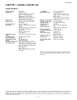
Page 3: ...he tray Legal 5 sheets Recommended paper weight is 20 lb Copy Bond Compatibility Input document size Effective scanning width Effective printing width Contrast control Reception modes Copy function Telephone function Power requirements Operating temperature Humidity Power consumption Dimensions without attachments Weight without attach ments ITU T CCITT G3 mode Automatic feeding Width 5 8 to 8 5 1...

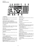
Page 4: ...ey has been pressed or the ringer volume at any other time FUNCTION key setting Press these keys after pressing the FUNC TION key to scroll through the FUNCTION MODE settings 8 Number keys Use these keys to dial numbers and enter numbers and letters when storing auto dial numbers 9 Panel release Press this release to open the operation panel 10 STOP key Press this key to cancel operations before t...

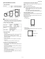
Page 5: ... insertion into the feeder to prevent possible double feeds 5 Automatic Document Feeder Capacity Number of pages that can be placed into the feeder at anytime is as follows Normal size max ADF 10 pages Special size single sheet only manual feed NOTE When you need to send or copy more pages than the feeder limit place additional pages in feeder when last page in feeder is being scanned Place additi...

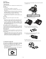
Page 6: ...pproximately 2 hours before using machine TELEPHONE JACK A standard RJ11C single line wall telephone jack must be located near the machine This is the telephone jack commonly used in most homes and offices Plugging the fax machine into a jack which is not RJ11C single line wall telephone jack may result in damage to the machine or your telephone system If you do not know what kind of jack you have...

Page 7: ...he power is turned on and off by simply plugging in or unplugging the power cord 3 Insert one end of the line cord into the jack on the back of the machine marked TEL LINE Insert the other end into a standard RJ11C single line wall telephone jack Setting the dial mode The fax machine is set for tone dialing If you are on a pulse dial line you must set the fax machine for pulse dial ing Press the k...

Page 8: ...has been set at the factory to scale received faxes to letter size paper If you loaded legal paper you must change the paper size setting to LEGAL 4 Print contrast setting You fax has been set at the factory to print at normal contrast If desired you can change the print contrast setting to LIGHT The stack should not be higher than this line Note If at any time the display shows the alternating me...

Page 9: ...the green levers on each side of the white roller 3 Gently and remove the document Be careful not to tear the document 4 Flip down the green levers on each side of the white roller Rotate the front gear until the film is taut and then close the operation panel press down on both sides to make sure it clicks into place 6 Clearing jammed printing paper 1 Open the operation panel press 2 Gently pull ...

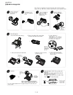
Page 10: ...t side down The stack should not be higher than this line GENTLY LOAD PAPER INTO THE PAPER TRAY DO NOT FORCE IT DOWN INTO THE FEED SLOT 1 3 Plug the power cord into a 120 V grounded outlet Connect the telephone line cord to the TEL LINE jack and a wall telephone jack Attach the paper tray and document support Note To enter your name and fax number and set the date and time so that they appear at t...

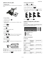
Page 11: ...umber and press 4 Enter a name by pressing number keys To enter two letters in succession that require the same key press after entering the first letter 5 Press and then 7 Option imaging film specifications 1 Structure This article is composed of polyester film coated with heat resistant layer matt layer and hot melt ink layer leader film and paper core Ink film specification is DNP standard ink ...

Page 12: ...ows the desired vol ume level 5 2 Handset 1 When talking through the handset press UP or DOWN key until the display shows the desired volume level 5 3 Ringer 1 Press the UP or DOWN key Make sure SPEAKER key has not been pressed the handset is not lifted and a document is not loaded in the feeder 2 If you selected RINGER OFF OK press START MEMORY key TEL LIU PWB POWER SUPPLY PWB CONTROL PWB CNMT CN...

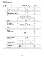
Page 13: ...stered content is sent 12 ENTRY DATA RECEIVE Registered content is received and its list is output Press FUNC 9 8 7 and the following display will appear ROM Ver TC89 After 2 sec DIAG MODE TC89 Then press the START key Select the desired item with the key or the key or select with the rapid key Enter the mode with the START key Diag specifications If the diag mode cannot be set repeat the diag mod...

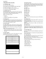
Page 14: ...o the default settings 3 8 Shading mode The mode is used for the shading compensation For reading set up the special original paper The compensation memorizes the reference data of white and black for reading Moreover the memorized data is not erased even if memory clear mode is executed 3 9 All black print This mode is used to check the state of the printing head and to inten tionally overheat it...

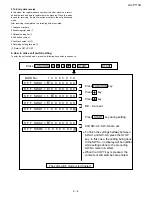
Page 15: ...itch mode press the following key entries in sequence Press FUNCTION 9 8 7 START START Press FUNCTION key Press key Press key Bit1 8 are set Soft SW A2 SW O6 are set S F T SW A1 1 0 0 0 0 0 0 0 S F T SW A1 1 0 0 0 0 0 0 0 S F T SW A1 1 0 0 0 0 0 0 0 S F T SW A1 1 0 0 0 0 0 0 0 S F T SW A2 0 0 0 0 0 0 0 0 S F T SW O6 0 0 0 0 0 0 0 0 Press key during setting To finish the settings halfway between SW...

Page 16: ...ode No Yes 0 7 Communication error treatment in TRN sending mode reception No communication error Communication error 0 8 CNG transmission No Yes 0 SW l A3 1 2 CED tone signal interval 1000ms 750ms 500ms 75ms 0 0 No 1 1 1 0 0 No 2 1 0 1 0 3 MR coding No Yes 0 4 Reserved 0 5 Reserved 0 6 Reserved 0 7 Reserved 0 8 Reserved 0 SW l A4 1 2 3 4 5 Signal transmission level 0 1 0 0 0 6 Protocol monitor Er...

Page 17: ...rved 0 4 Busy tone detection after auto dial No Yes 0 5 6 Waiting time after dialing 45 sec 55 sec 90 sec 140 sec 0 0 No 5 0 0 1 1 No 6 0 0 1 1 7 Reserved 0 8 Reserved 0 SW l B3 1 Reserved 0 2 Reserved 0 3 Reserved 0 4 Reserved 0 5 Reserved 0 6 7 Auto dial mode delay timer of before line connect 0 sec 1 5 sec 3 0 sec 4 5 sec 0 0 No 6 0 0 1 1 No 7 0 1 0 1 8 Hold key Enable Disable 1 SW l B4 1 2 Aut...

Page 18: ...ection in half tone mode No Yes 0 8 Reserved 0 SW l D1 1 2 3 4 Number of rings for auto receive 0 1 0 0 OPTION 5 Automatic switching manual to auto receive mode Reception after 5 rings No reception 0 6 Reserved 0 7 8 Cl detect frequency As PTT 11 5Hz 13 0Hz 20 0Hz 0 0 No 7 0 0 1 1 No 8 0 1 0 1 SW l D2 1 2 3 Distinctive ringing setting PATTERN 4 and 5 are for CANADA only No 1 No 2 No 3 0 0 0 OPTION...

Page 19: ...eserved 0 3 Reserved 0 4 Reserved 0 5 Reserved 0 6 Reserved 0 7 Reserved 0 8 Reserved 0 SW l F1 1 2 DTMF detection time 50ms 80ms 100ms 120ms 0 0 No 1 0 0 1 1 No 2 0 1 0 1 3 Protection of remote reception 5 detect Yes No 1 4 Remote reception with GE telephone Compatible Not compatible 1 5 6 7 8 Remote operation code figure by external TEL 0 9 0 1 0 1 SW l F2 1 CNG detection in STAND BY mode Yes No...

Page 20: ... Reserved 0 3 Reserved 0 4 Reserved 0 5 Reserved 0 6 Reserved 0 7 Reserved 0 8 Reserved 0 SW l H1 1 Reserved 0 2 Reserved 0 3 Reserved 0 4 Reserved 0 5 Reserved 0 6 Reserved 0 7 Reserved 0 8 Reserved 0 SW l H2 1 Reserved 0 2 Reserved 0 3 Reserved 0 4 Reserved 0 5 Reserved 0 6 Reserved 0 7 Reserved 0 8 Reserved 0 SW l I1 1 Reserved 0 2 Reserved 0 3 Reserved 0 4 Reserved 0 5 Reserved 0 6 Reserved 0 ...

Page 21: ...d 0 3 Reserved 0 4 Reserved 0 5 Reserved 0 6 Reserved 0 7 Reserved 0 8 Reserved 0 SW l I7 1 Reserved 0 2 Reserved 0 3 Reserved 0 4 Reserved 0 5 Reserved 0 6 Reserved 0 7 Reserved 0 8 Reserved 0 SW l J1 1 Reserved 0 2 Reserved 0 3 Sender s phone number setting Cannot change Change allowed 0 4 Reserved 0 5 Reserved 0 6 Summer time setting No Yes 1 OPTION 7 8 Ringer volume Off Low Middle High 1 0 OPT...

Page 22: ...A4 paper enable Enable Disable 0 7 LEGAL LETTER paper enable Enable Disable 1 8 Reserved 0 SW l L2 1 2 Paper set size LETTER LEGAL A4 0 0 OPTION No 1 0 0 1 No 2 0 1 0 3 Automatic reduce of receive Auto 100 1 OPTION 4 5 6 Print contrast Normal Lighter Light Dark Darker 1 0 0 OPTION No 4 0 0 0 0 1 No 5 0 0 1 1 0 No 6 0 1 0 1 0 7 Reception reduction ratio in case of memory full 100 93 0 8 Reserved 0 ...

Page 23: ...2 Reserved 0 3 Reserved 0 4 Reserved 0 5 Reserved 0 6 Reserved 0 7 Reserved 0 8 Reserved 0 SW l O2 1 Reserved 0 2 Reserved 0 3 Reserved 0 4 Reserved 0 5 Reserved 0 6 Reserved 0 7 Reserved 0 8 Reserved 0 SW l O3 1 Reserved 0 2 Reserved 0 3 Reserved 0 4 Reserved 0 5 Reserved 0 6 Reserved 0 7 Reserved 0 8 Reserved 0 SW l O4 1 Reserved 0 2 Reserved 0 3 Reserved 0 4 Reserved 0 5 Reserved 0 6 Reserved 0...

Page 24: ...UX P115U 2 13 SW l O6 1 Reserved 0 2 Reserved 0 3 Reserved 0 4 Reserved 0 5 Reserved 0 6 Reserved 0 7 Reserved 0 8 Reserved 0 SW NO DATA NO ITEM Switch setting and function Initial setting Remarks 1 0 C ...

Page 25: ... transmit SENDER S INFORMATION TRANSMISSION is a switch to set the function to print the content of HEADER PRINT described in the pass code list at the front end of receiver s original when original is sent to the remote machine If this switch is set to NO the HEADER PRINT is not output at the receiving machine SW A2 No 6 H2 mode Used to determine reception of H2 mode 15 sec transmission mode When...

Page 26: ...lback when RX level is under 40dBm When set to 1 if fax signal level is under 40dBm during reception machine selects the slower modem speed automatically It is effective when noises occur on the received document due to the long distance communications SW B1 No 1 No 4 Recall interval Choice is made for a redial interval for speed and rapid dial calls Use a binary number to program this If set to 0...

Page 27: ...he hook to have the facsimile start receiving If it was set to 0 accidentally receive ring is set to 1 NOTE If the machine is set to answer after a large number of rings it may not be able to receive faxes successfully If you have diffi culty receiving faxes reduce the number of rings to a maxi mum of 6 SW D1 No 5 Automatic switching manual to auto receive mode This soft switch is used to select w...

Page 28: ...eption 5 When set to 1 the remote reception function is disabled SW F1 No 4 Remote reception with GE telephone Corresponding to TEL mode by GE P B X 1 Compatible with TEL mode by GE 0 Not compatible When sending 5 for remote reception with a GE manufac tured telephone remote reception may not take place because of special specifications in their DTMF To overcome this a soft SW is provided to chang...

Page 29: ...g communication error alone If No 2 0 No 3 1 No 4 0 are set printing is always on printed even if it is normally ended 000 Error timer and memory sending receiving 001 Sending 010 Continuous printing 011 Not printed 100 Communication error SW J3 No 5 No 8 Reserved Set to 0 SW K1 No 1 No 8 Reserved Set to 0 SW L1 No 1 No 4 Reserved Set to 0 SW L1 No 5 Cut off mode COPY mode Whether the excessive pa...

Page 30: ... 2 19 SW O1 No 1 No 8 Reserved Set to 0 SW O2 No 1 No 8 Reserved Set to 0 SW O3 No 1 No 8 Reserved Set to 0 SW O4 No 1 No 8 Reserved Set to 0 SW O5 No 1 No 8 Reserved Set to 0 SW O6 No 1 No 8 Reserved Set to 0 ...

Page 31: ... follow ing format and check the related matters TO ATT Ref No CC ATT Date FM Dept Sign Please complete this report before calling the TAC hotline if problem still occurs Facsimile communication problem Ref No Date From Mr Fax Tel No Our customer Name Tel No Address Fax No Contact person Model name Other party Name Tel No Address Fax No Contact person Model name Problem mode Line Domestic internat...

Page 32: ...mpossible 12 Error occurred just after fallback 13 Error occurred after a response to retransmission end command was received Code Final received signal Error Condition Receiver side 0 Incomplete signal frame Cannot recognize bit stream after flag 1 NSS DCS Cannot recognize CFR or FTT signal Disconnects line during transmission line error 2 NSC DTC Cannot recognize NSS signal FIF code etc 3 EOP Ca...

Page 33: ...ooth feeding of the document 2 Document separation method Separate plate 3 3 Documents applicable for automatic feed NOTE Double side coated documents and documents on facsimile recording paper should be inserted manually The document feed quantity may be changed according to the document thickness Documents corresponding to a paper weight heavier than 70 kg 80 g m2 and lighter than 135 kg 157 g m...

Page 34: ...g paper feed roller and the recording paper The main scanning is electronically performed and the sub scanning is mechanically performed by sending the recording paper with the recording paper feed roller 5 2 3 Recording paper transfer sequence 1 The recording paper stored in the paper tray ass y is fed with the PU roller and is stopped when the P IN sensor is turned on by sensing its lead edge 2 ...

Page 35: ...of the product the disassembly and the assembly procedures should be performed carefully and deliberately Fig 1 Bottom plate PWB s and drive unit 1 Parts list Fig 1 9 Connector 1 10 TEL LIU PWB unit 1 11 Connector 6 12 Screw 3x10 1 13 Hook 1 14 Control PWB unit 1 15 Wire holder PWB 1 16 Screw 3x10 2 17 Drive unit 1 No Part name Qty No Part name Qty 1 Mechanism uni 1 2 Screw 3x10 5 3 Screw 1 4 AC c...

Page 36: ...w 3x12 4 6 Operation panel unit 1 7 Screw 3x10 2 8 Hook 7 9 Top cover unit 1 10 Sub frame unit 1 No Part name Qty No Part name Qty 1 Mechanism unit 1 2 Stopper plate 1 3 Operation panel unit top cover unit sub frame unit 1 4 Panel cable cover 1 NOTE For disassembly of the inside of the unit refer to the exploded view in the parts guide NOTE When removing the operation panel unit detach the stopper...

Page 37: ...Qty 1 Mechanism unit 1 2 Screw 3x10 1 3 CIS unit 1 4 Head cover 1 5 Thermal head unit 1 NOTE For disassembly of the inside of the unit refer to the exploded view in the parts guide Hook Hook Hook Screwdriver 2 3 4 5 CIS unit Thermal head unit 400 g 700 g 800 g 700 g 200 g 200 g 400 g 1 Mechanism unit ...

Page 38: ...eaker Motor cable Cam switch cable Speaker cable CIS cable Panel cable Head cable Rib Cam switch cable Rib Motor cable Drive unit Top cover unit Operation panel unit Panel cable Thermal head Head cable Head cable Tape Rib Rib Rib CIS cable Scanner frame Tape TEL LIU PWB Drive unit 1 2 2 Figure for setting the Speaker Hold Spring Speaker Hold Spring Speaker Panel cable Rib Wire hold PWB ...

Page 39: ...OL PWB UNIT 1CHIP FAX ENGINE SCE209 HANDSET SPEAKER 24V OPERATION PANEL TEL LIU PWB UNIT DRIVER MOTOR CONTACT IMAGE SENSOR DOCUMENT SENSOR PIO POWER SUPPLY PWB UNIT AMPLIFIER DSP SURGE PROTECT FILTER CML TRANSFORMER CI VBT STABILIZER RECTIFIER TRANSFORMER RECTIFIER DIODE TRANS SURGE ABSORBER FILTER LINE CLOCK 32 256MHz LCD FET THERMAL HEAD P IN SENSOR FILM SENSOR RECORDING PAPER FRONT SENSOR SIO S...

Page 40: ...ONTACT IMAGE SENSOR LCD UNIT CNLCD OPERATION PANEL PWB NUIT 14 CNPN A 15 7 CNCSW CNMT CNTH CNCIS CNPN CNSP SPEAKER CNLIUA CNPW 12 6 CONTROL PWB UNIT TEL LIU PWB UNIT POWER SUPPLY PWB UNIT CNLIUA CNPS TEL LINE MJ1 MJTEL AC CORD TX RX MOTOR 3 HANDSET 4 16 CNPRG ...

Page 41: ...V VO VG CISVDD øT CISCLK GLED 24V KEN4A KEN3A KEN2A KEN1A DG 3 3V ORGSNS FRSNS E SEN0 SEN1 SEN2 SEN3 SEN4 SEN5 SEN6 CNPN CNCIS 1 2 3 4 5 6 7 8 9 10 11 12 1 2 3 4 5 6 7 8 9 10 11 12 TEL LIU PWB RHS DG 24VL MICMUTE TELIN TELMUTE RXIN TXOUT CML PIN FILM CI RHS MAG 24VL MICMUTE TELIN TELMUTE RXIN TXOUT CML PIN FILM CI CNLIUA CNLIUA CNMT CNTH 1 2 3 4 5 6 1 2 3 4 5 6 POWER SUPPLY PWB 24V 24V MG MG DG VR...

Page 42: ... RAM The data is then con verted from parallel to serial form by the modem where the serial data is modulated and sent onto the line Receive operation There are two ways of starting reception manual and automatic Depression of the START key in the off hook mode in the case of manual receive mode or CI signal detection by the LIU in the auto matic receive mode First the SCE209 controls the procedur...

Page 43: ...ash memory The supported size of NOR type memory is up to 1 MB and the supported size of NAND type memory is unlimited 2 2 6 Stepper Motor Control Eight outputs are provided to external current drivers four to the scan ner motor and four to the printer motor The stepping patterns are pro grammable and selectable line times are supported A timeout circuit controls the power control of the motors Th...

Page 44: ...gh frequency as a modulation frequency the output level can be made programmable 2 2 18 Watchdog Timer The Programmable Watchdog Timer is intended to guard against firm ware lockup on the part of either executive controlled background tasks or interrupt driven tasks and can only be enabled by a sequence of events under control of the Watchdog Control Logic Once the Watchdog Timer has been enabled ...

Page 45: ...17 O 1XC 24 VDD Digital Power 25 RASn O 13Xs 26 CAS 0 n O 13Xs 27 DWRn O 13Xs 28 VBAT RTC Battery Power 29 XIN I Osc1 30 XOUT O Osc1 31 WRPROTn O 1XC 32 TEST 1 I Hd 33 TEST 0 I Hd 34 BATRTSn I H 35 INTPWRDWNEn I H 36 PWRDWNn I O H 13Xs 37 N C 38 ADGA VADG PADC Analog GND 39 VREFn CLREF I VR PADC 40 VIN I VA PADC 41 ADGA VADG PADC Analog GND 42 ADVA VADV PADC Analog Power 43 ADXG VXG PADC 44 VREFp ...

Page 46: ...river Output 90 DVDD PWD IA Digital Power 91 MODE_0 ID u Connect to VSS IA Mode Selection 92 ICLK I OD IA Bit Clock Input Output 93 VSS VSS Digital GND 94 FCSn 1 VIDCTL 0 GPO 23 O 13Xs 95 IARESET O 13Xs DSP to EXTIA POR 96 IACLK O 13Xs DSP to EXTIA MCLK 97 VDD Digital Power 98 IA1CLK I H DSP from EXTIA ICLK 99 SR3IN DSPIRQn I H DSP from primary EXTIA SOUT EXT Modem IRQn 100 SR4OUT O 13Xs DSP to pr...

Page 47: ...s CPU Data Bus 142 D 1 I O Tu 13Xs CPU Data Bus 143 D 2 I O Tu 13Xs CPU Data Bus 144 D 3 I O Tu 13Xs CPU Data Bus 145 D 4 I O Tu 13Xs CPU Data Bus 146 D 5 I O Tu 13Xs CPU Data Bus 147 D 6 I O Tu 13Xs CPU Data Bus 148 D 7 I O Tu 13Xs CPU Data Bus 149 GPIO 20 ALTTONE I O Hu 13Xs 150 GPIO 26 I O Hu 13Xs 151 GPIO 27 I O Hu 13Xs 152 GPIO 28 I O Hu 13Xs 153 GPO 26 O 13Xs 154 GPO 27 O 13Xs 155 GPO 28 O 1...

Page 48: ...CRYSTAL SCANNER CONTROLS SENSORS START CLK2 CLK1 CLK1N VIDCTL 1 0 XIN XOUT INTERNAL IA LINE INTERFACE DRAM SCANNER VIDEO PREPROCESSING SERIAL SYNC PORTS SSIF VIN VREFP VREFN SSCLK 2 1 SSTXD 2 1 SSRXD 2 1 SSSTAT 2 1 SYNC ASYNC SERIAL PORT SASIF SASCLK SASTXD SASRXD GPIO GENERAL PURPOSE I O DEBUGN VDD VDRAM VBAT VSS FLASH MEMORY OPTION WRPROTN FRDN FRWN FCLE FCSN 2 0 D 7 0 RDN A 23 0 WRN ROMCSN CS 5...

Page 49: ... the SIA The following table the PIA SIA control register RAM access code For changes made to IACR1 to be effective the host must write to IAADD with a value of 0002h For changes made to IACR2 to be effective the host must write to IAADD with a value of 0006h For changes made to IACR3 to be effective the host must write to IAADD with a value of 0007h Configuration default values are shown below Th...

Page 50: ...ion Ringer volume It is controlled by the combination of the attenuator value of the LINE DRIVER in the modem and the ringer sending level sent from the modem Speaker volume It is controlled by the attenuator value of the LINE DRIVER in the modem 4 Ringer circuit section The ringer sound is formed in the tone of modem when CI signal is detected The amplifier circuit drives the speaker of the main ...

Page 51: ... generating relay H Line make L Line break SP MUTE The circuit is located in the TEL LIU PWB Speaker tone mute control signal H Muting Power down mode L Muting cancel Normal operation TELMUTE Handset reception mute control signal H Muting L Muting cancel RCVOL DTMFMUTE The circuit is located in the control PWB Handset receiver volume control signal Note The DTMF sending listed above is DTMF signal...

Page 52: ...ignal Name CNLIUA NO Signal Name CNLIUA 1 RHS 7 RXIN 2 MAG 8 TXOUT 3 24VL 9 CML 4 MICMUTE 10 PIN 5 TELIN 11 FILM 6 TELMUTE 12 CI DAC LPF DAC H L CI DETECTOR SPEAKER LINE 24VL DG CONTROL PWB TEL LIU PWB RX TX TEL MUTE H MUTE PC1 Q102 IC100 Q103 IC100 IC100 IC100 IC4 0 1 0 0 1 0 1 1 RTLOOP ADC SIN MIC LINE SELECT SP OUT ENABLE MIC ENABLE LINE IN ENABLE LINE OUT ENABLE 0 20 25 30dB LINE SELECT 1 1 0 ...

Page 53: ...inging Q1 to OFF state through detection of voltage of T1 subwinding The over voltage protection is performed by operating the over current protection circuit through detection of Zener diode ZD4 and short cir cuiting of load 5 Circuit description of CIS unit 1 CIS CIS is an image sensor which puts the original paper in close contact with the full size sensor for scanning being a monochromatic typ...

Page 54: ...REGDMA GPO18 CLKDIV0 175 WAIT GPO19 CLKDIV1 176 RAS 25 CAS 26 DWR 27 WRPROT 31 BATRST 34 VBAT 28 PWRDWN 36 INTPWRDOWNE 35 XOUT 30 XIN 29 VREFp 44 VREFn CLREF 39 VIN 40 THADI 49 ALTTONE BZ 149 OPI0 19 OPI1 20 OPI2 21 OPI3 22 SM0 171 SM1 172 SM2 173 SM3 174 OPO0 12 OPO1 13 OPO2 14 OPO3 15 OPO4 16 OPO5 17 OPO6 18 SXIN 10 SXOUT 11 CLK2 69 START 67 STRB0 57 STRB1 58 STRB2 59 STRB3 60 PCLK 63 PDAT 62 PL...

Page 55: ...I 1 3I 1 3I 1 3I IC2 DRAM VCC 1 WE 7 RAS 8 A9 9 VCC 14 GND 15 OE 22 CAS 23 GND 28 DQ0 2 DQ1 3 DQ2 4 DQ3 5 DQ4 24 DQ5 25 DQ6 26 DQ7 27 A0 10 A1 11 A2 12 A3 13 A4 16 A5 17 A6 18 A7 19 A8 20 NC 6 NC 21 R121 10k C111 0 1u 25V IC1 FLASH ROM SST39VF020P A0 20 A1 19 A2 18 A3 17 A4 16 A5 15 A6 14 A7 13 A8 3 A9 2 A10 31 A11 1 A12 12 A13 4 A14 5 A15 11 A16 10 A17 6 CE 30 OE 32 WE 7 D0 21 D1 22 D2 23 D3 25 D...

Page 56: ...3 SCE209 2 2 MODEM BLOCK GPIO15 CS5 53 GPIO16 52 AVDD IIA 85 GPIO37 55 GPO28 155 GPIO31 159 GPO27 154 GPO25 68 GPIO34 162 GPO30 157 GPIO32 160 GPIO13 54 GPIO17 51 SPKR_OUTP IIA 88 GPO1 168 MIC_INM IIA 81 MIC_INP IIA 80 GPO29 156 MODE 0 91 GPO0 167 LINE_INP IIA 79 N C 37 SASRXD 110 GPIO3 109 GPIO19 66 GPIO11 65 GPIO36 164 GPIO35 163 VTHON 56 MIC_BIAS IIA 82 TESTC 73 FCS 94 GPIO29 158 SASCLK2 105 DS...

Page 57: ...NS PHTSNS ORGSNS DG VREG DG 24V 24V DG DG FG MG DG DG DG DG MG MG 3 3A 1 1G 3 3A 3 3A R102 270 C182 0 1u25V 3 3V D101 1SS355 A K R179 N M N M N M BAT1 CR2032 C201 DG C104 1000p 50V 2 5 IC 6 4 3 1 R108 DG C202 R140 51K REG1 S 814A33AUA Vin 3 Vout 1 VSS 2 R150 N M N M R181 R180 R183 R110 N M C167 0 1u 50V D100 HRW0202 A1 A2 K C6 47u 25V R100 5 6K VBT1 C194 1000p 50V C3 220u 6 3V R182 C10 22u 50V C16...

Page 58: ...0W 300W 2W 0 01u 50V 1000p 50V ROHM DYNA 5 5i 3 2A 5 3D DG DG DG DG DG DG THG THG DG DG MG MG C109 0 1u 25V R1 N M C150 N M C110 0 1u 50V R169 1K C1 220u 6 3V VO R136 470K VIN R112 1K R137 20K D1 D2 D3 D4 S1 S2 S3 G Q107 SI4431BDY 4 5 8 3 1 2 6 7 IC5 ULN2001A E 8 1B 1 2B 2 3B 3 4B 4 5B 5 6B 6 7B 7 7C 10 6C 11 5C 12 4C 13 3C 14 2C 15 1C 16 COM 9 Q101 RT1N141C B C E VG C166 R168 120k ZD1 1N4748 R173...

Page 59: ... 3 3H 3 6A N C DG DG DG DG DG RXIN 3 3H 3 2H 3 3A C157 1u 10V K C200 0 1u 25V Q104 RT1N141C B C E R116 20k NJM2113 IC4 5 4 3 2 1 7 8 6 R118 120k C177 0 1u 16V K C175 1u 10V K D102 1SS355 C176 0 R157 7 5k R133 100k C180 R119 20k Q103 RT1N141C B C E C131 1u 10V R158 C132 1u 10V R156 1M C178 0 1u 16V K Q106 B C E C2 47u 25V 1 2 R120 220k C159 1u 10V K C179 C133 220p 50V R117 1k D103 Q105 B C E R167 3...

Page 60: ...UX P115U 6 7 7 Control PWB parts layout Top side ...

Page 61: ...UX P115U 6 8 8 Control PWB parts layout Bottom side ...

Page 62: ...13 N M N M N M PC1 PC817X4 2 1 AR 1 RA391P V6 2 C108 N M ZD5 HZ9C3 TP2 J23 JP C114 2200p R100 3 3k C101 0 1u C103 1000p AR 3 RA501P C6 R106 82K L2 R1 100 1 2W Q102 RT1N436C R123 1 5K R117 8 2K PH2 PIN 2 1 4 3 J24 JP R124 1K IC100 LM2902NS 8 10 9 C110 1000p CML OUAZ SH 124DZ TP4 PC1 PC817X4 4 3 IC100 7 5 6 Q1 KTC3198GR C111 220p D1 1N4148 A K R7 22k 1 2W TP3 11 4 IC100 LM2902NS 1 2 3 Q100 RT1N436C ...

Page 63: ...UX P115U 6 10 2 TEL LIU PWB parts layout Top side The TEL LIU PWB of the model employs lead free solder ...

Page 64: ...UX P115U 6 11 3 TEL LIU PWB parts layout Bottom side The TEL LIU PWB of the model employs lead free solder ...

Page 65: ...D GND 1 2 6 3 4 5 6 8K N M R27 6 8K R29 6 8K ZD4 HZ30CPTK ZD9 RD9 1ESAB2 T1 ZD8 RD10ESAB T1 R13 4 7K R14 1K R16 10K C12 0 1 VR1 2 2K R17 3 3K ZD5 RD6 2SAB2 T1 R15 330K Q4 2SC1740S R18 3 3K PC1 PS2501 1L C10 330 16 D8 ERA81 004V3 D7 S3L20U FB3 BP53RB052025050 D9 ERA22 06V3 R3 470K C26 C3 470P Q1 2SK3306 ZD1 27HSB 26 C27 0 01 0 01 L1 33mH 0 5A C1 0 22 V1 S07K150GA F1 R10 R9 47 Q3 2SC1741AS R8 47K 0 ...

Page 66: ...UX P115U 6 13 2 Power supply PWB parts layout Top side 3 Power supply PWB parts layout Bottom side ...

Page 67: ... sw22 sw15 sw16 sw23 sw20 sw27 sw24 sw26 CNLCD 4 CNLCD 6 CNLCD 1 CNLCD 13 CNLCD 12 CNLCD 2 CNLCD 14 CNLCD 11 CNLCD 5 CNLCD 3 E KEN4A CNPN RS E CNLCD 6 3 3V 4 1 R W 9 VO N C 8 2 7 5 3 LD2 LD1 10 LD0 LD3 11 12 13 14 CNPN 1 CNPN 4 CNPN 2 CNPN 3 SEN2 SEN3 SEN0 SEN4 KEN3A KEN1A KEN2A SEN5 3 3V ORGSNS FRSNS SEN1 DG N C N C N C SEN6 DG 6 2 12 7 14 13 5 10 11 1 8 9 3 4 15 16 D 5 1N4148 A K 5 8 START R4 10...

Page 68: ...UX P115U 6 15 2 Operation panel PWB parts layout Top side Since the parts of PWB cannot be supplied change it as a unit The Operation panel PWB of the model employs lead free solder ...

Page 69: ...UX P115U 6 16 3 Operation panel PWB parts layout Bottom side Since the parts of PWB cannot be supplied change it as a unit The Operation panel PWB of the model employs lead free solder ...

Page 70: ...CF DCN CFR TSI CSI CSI TSI RTC EOP MCF DCN IMAGE SIGNAL Document ejected Recording paper ejected Receive side G3 communication CED Transmitter side Document inserted into document sensor during standby To recording position DCS Cut line printed IMAGE SIGNAL Cut line printed IMAGE SIGNAL IMAGE SIGNAL Next page insert command 1st page Document inserted to the reading position DCS ...

Page 71: ...nitialized STOP key ÒWAIT A MOMENTÓ display START NO YES STAND BY 3 sec NO ÒMEMORY CLEAR Ó display NO YES STAND BY 3 sec NO NO START key COPY key STOP key NO Memory clear STAND BY 2 1 ÒMEMORY CLEAREDÓ display Memory clear PROCESS CHECK MODE ÒMEMORY CLEAREDÓ display YES ...

Page 72: ... PRICE RANK 1 QCNWG471BSCZZ SPEAKER RELAY CABLE 1 AN 2 QCNWG206BSCZZ PANEL RELAY CABLE 1 AT 3 QCNWG202BSCZZ CIS RELAY CABLE 1 AN 4 QCNWG205BSCZZ HEAD RELAY CABLE 1 AS 5 QCNWG204BSCZZ CAM SWITCH RELAY CABLE 1 AG 6 QCNWG242BSCZZ MOTOR RELAY CABLE 1 AM 7 QCNWG201BSCZZ SENSOR RELAY CABLE 1 BB 8 VRS RE3AA122J RESISTOR 1W 1 2KΩ 5 R30 1 AC 9 VHPSG206S 1 PHOTO TRANSISTOR PH1 1 AG 10 VHPSG206S 1 PHOTO TRAN...

Page 73: ...et the test PWB switches to the fixed position Mechanical unit PWB to be tested Actual operation with mechanical unit PWB sensor check POWER SUPPLY PWB CHECK TEL LIU PWB CHECK CONTROL PWB RELAY CABLE DON T SEPARATE UNIT NOTE PAPER SENSOR RELAY CABLE QCNWG201BSCZZ TO CHECK PWB TO EXTENSION PWB PIN TP1 FILM TP2 DG TP3 24VL TP4 TEL LIU TEL LIU TEL LIU TEL LIU BROWN RED ORANGE YELLOW ON OFF operation ...

Page 74: ... and black basis is applied to remember the shading waveform Be sure to perform this operation when replacing the battery or replacing the control PWB Execute in the shading mode of DIAG mode SHADING WAVE MEMORY STANDARD PAPER PSHEZ3579SCZZ ...

Page 75: ... PGiDM2629XHZZ which shows in the drawing Remove A4 guide when you use the record paper of the letter size 2 Set soft switch SW L2 No 1 and the initialization of SW L2 No 2 as follows Hook Paper tray ass y A4 Guide PGiDM2629XHZZ SW NO DATA NO ITEM Switch setting and function Initial setting Remarks 1 0 SW l L2 Paper set size LETTER LEGAL A4 OPTION 1 No 1 0 0 1 0 2 No 2 0 1 0 0 ...

Page 76: ...UX P115U 8 5 MEMO ...

Page 77: ...of the set UX P115U UX P115 This document has been published to be used for after sales service only The contents are subject to change without notice MODEL SELECTION CODE DESTINATION UX P115 U U S A 1 Cabinet etc 2 Top cover Sub frame 3 Upper cabinet Document guide upper 4 Drive unit 5 Packing material Accessories 6 Control PWB unit 7 TEL LIU PWB unit 8 Power supply PWB unit 9 Operation panel PWB...

Page 78: ...TION PANEL UNIT 62 DOCUMENT GUIDE UPPER TOP COVER SUB FRAME DRIVE UNIT 27 22 30 31 28 25 26 26 29 4 57 35 54 46 50 52 51 53 3 5 36 37 58 48 47 6 16 17 49 41 42 45 7 61 44 43 59 29 25 24 33 34 32 63 23 64 65 67 8 68 B2 B1 B1 B1 B1 B1 B1 B2 B3 B2 W1 B4 B1 W2 ...

Page 79: ...B C Head spring B 40 MSPRC3340XHZA AD C Head spring C 41 PCOVP2130XHZZ AE C Head cover 42 PGIDM2615XHZZ AD C Head guide left 43 PGIDM2616XHZZ AD C Head guide right 44 QCNWN486AXHZZ AM C Head cable 45 RHEDZ2065XHZZ BP B Thermal head 46 GCOVA2447XHVA AL D Front cover 47 GLEGG2078XHZZ AD C Rubber leg 48 LPLTM3178XHZZ AF C Bottom plate 49 LPLTP3177XHZZ AD C Stopper plate 50 MLEVP2357XHZZ AD C Film sen...

Page 80: ... C PU roller 15 NSFTP2357XHZZ AG C Paper feed roller shaft 16 NSFTP2374XHZZ AG C PU roller shaft 17 PGIDM2621XHSA AF C Release lever 18 LHLDZ2224XHZZ AL C RP feed plate holder 19 LPLTG3181XHZZ AD C RP separate rubber 20 LPLTP3179XHZZ AD C RP separate base 21 LPLTP3180XHZZ AH C RP separate plate 22 LPLTP3182XHZZ AH C RP feed plate 23 MSPRC3299XHZZ AB C RP separate spring 24 MSPRC3300XHZZ AB C RP fe...

Page 81: ...AE C ORGSNS sensor 9 QCNWN399BXHZZ AP C Panel cable 10 RUNTZ2127XH01 BC N E LCD unit 11 LPLTG2911XHZZ AE C Separate rubber 12 LPLTP3175XHZZ AD C Separate plate 13 LPLTP3176XHZZ AD C Feed plate 14 MSPRD3293XHZZ AB C Separate spring 15 MSPRT3294XHZZ AB C Feed spring 16 PGIDM2614XHSA AL C Document guide upper 17 PSHEP3660XHZZ AE C Separate rubber sheet 18 JBTN 2360XHSC AH C Speed key 19 JBTN 2361XHSD...

Page 82: ... hold spring 10 NGERH2380XHZZ AC C Reduction gear 17 36Z 11 NGERH2409XHZZ AB C Idler gear 23Z 12 NGERH2571XHZZ AD C Slip gear 13 NGERH2572XHZZ AD C Reduction gear 25 63Z 14 NGERH2573XHZZ AD C Reduction gear 20 40Z 15 NGERH2574XHZZ AD C Reduction gear 15 30Z 16 NGERH2575XHZZ AD C Idler gear 40Z 17 NGERH2576XHZZ AD C Idler gear 21Z 18 NGERH2577XHZZ AD C Idler gear 20Z 19 NGERH2582XHZZ AC C Idler gea...

Page 83: ...r tray ass y 21 CGERH2566XH01 AG C Imaging film gear ass y 23 TCADZ2891XHZZ AF D Registration card 24 TCADZ3744XHZZ AL N D Setup guide 6 Control PWB unit 1 UBATL2049SCZZ AF B Battery CR2032T23 BAT1 2 VCEAGA0JW227M AD C Capacitor 6 3WV 220µ F C1 3 VCEAGA1EW476M AA C Capacitor 25WV 47µ F C2 4 VCEAGA0JW227M AD C Capacitor 6 3WV 220µ F C3 5 VCEAGA1HW106M AA C Capacitor 50WV 10µ F C4 6 VCEAGA1HW106M AA...

Page 84: ...1µ F C154 54 VCKYCY1HF104Z AA C Capacitor 50WV 0 1µ F C155 55 VCKYCY1AB105K AB C Capacitor 10WV 1µ F C157 56 VCKYCY1AB105K AB C Capacitor 10WV 1µ F C159 57 VCKYCY1HB102K AA C Capacitor 50WV 1000PF C160 58 VCKYCY1AF105Z AC C Capacitor 10WV 1µ F C161 59 VCKYCY1AF105Z AC C Capacitor 10WV 1µ F C162 60 VCCCCY1HH101J AA C Capacitor 50WV 100PF C163 61 VCKYCY1HF104Z AA C Capacitor 50WV 0 1µ F C167 62 VCCC...

Page 85: ...3 140 VRS CY1JB000J AA C Resistor 1 16W 0Ω 5 R134 141 VRS CY1JB103J AA C Resistor 1 16W 10KΩ 5 R135 142 VRS CY1JB474J AA C Resistor 1 16W 470KΩ 5 R136 143 VRS CY1JB203J AA C Resistor 1 16W 20KΩ 5 R137 144 VRS CY1JB224J AA C Resistor 1 16W 220KΩ 5 R139 145 VRS CY1JB513J AA C Resistor 1 16W 51KΩ 5 R140 146 VRS CY1JB271J AA C Resistor 1 16W 270Ω 5 R141 147 VRS CY1JB106J AA C Resistor 1 16W 10MΩ 5 R14...

Page 86: ...1N436C 1 AD B Transistor RT1N436C Q102 38 VSRT1N436C 1 AD B Transistor RT1N436C Q103 39 VRS RE2HA101J AB C Resistor 1 2W 100Ω 5 R1 40 VRS RE3AA122J AC C Resistor 1W 1 2KΩ 5 R2 41 VRD HT2HY202J AA C Resistor 1 2W 2KΩ 5 R3 42 VRS HT3AA510J AA C Resistor 1W 51Ω 5 R4 43 VRD HT2EY101J AA C Resistor 1 4W 100Ω 5 R5 44 VRD HT2EY151J AA C Resistor 1 4W 150Ω 5 R6 45 VRD HT2HY223J AA C Resistor 1 2W 22KΩ 5 R...

Page 87: ... 35 0CBUAC0264AK AD B Transistor 2SC1741AS Q3 36 0CBUAC0034EL AD B Transistor 2SC1740S Q4 37 0CBUEXDAW334 AC C Resistor 1 4W 330KΩ 5 R1 38 0CBUEXDAW474 AC C Resistor 1 4W 470KΩ 5 R2 39 0CBUEXDAW474 AC C Resistor 1 4W 470KΩ 5 R3 40 0CBUEEB681CT AC C Resistor 1 4W 680Ω 5 R4 41 0CBUEXCAP272 AC C Resistor 1 10W 2 7KΩ 5 R5 42 0CBUEXBAF183 AC C Resistor 1 16W 18KΩ 5 R6 43 0CBUEXBAF181 AC C Resistor 1 16...

Page 88: ...35XHZZ 2 30 AD C MSPRC3340XHZA 1 40 AD C MSPRC3346XHZZ 1 66 AD C MSPRC3357XHZZ 1 67 AD C MSPRD3285XHZZ 1 53 AB C MSPRD3286XHZA 1 52 AB C MSPRD3291XHZZ 1 54 AD C MSPRD3292XHZA 1 55 AB C MSPRD3293XHZZ 3 14 AB C MSPRD3298XHZZ 4 9 AE C MSPRD3302XHZZ 2 10 AB C MSPRD3341XHZZ 1 65 AD C MSPRD3379XHZZ 1 26 AD C MSPRP3297XHZZ 4 23 AD C MSPRT3294XHZZ 3 15 AB C N NGERH2380XHZZ 4 10 AC C NGERH2409XHZZ 4 11 AB ...

Page 89: ... 7 3 AA C VCEAGA1HW225M 7 6 AA C VCEAGA1HW226M 6 10 AB C 7 4 AB C 7 5 AB C VCEAGA1HW475M 7 9 AA C VCKYCY1AB105K 6 55 AB C 6 56 AB C 6 66 AB C PARTS CODE No PRICE RANK NEW MARK PART RANK VCKYCY1AF105Z 6 35 AC C 6 36 AC C 6 38 AC C 6 39 AC C 6 42 AC C 6 45 AC C 6 46 AC C 6 47 AC C 6 48 AC C 6 49 AC C 6 50 AC C 6 58 AC C 6 59 AC C VCKYCY1CB104K 6 65 AB C 6 68 AB C 6 69 AB C VCKYCY1HB102K 6 11 AA C 6 ...

Page 90: ... CY1JB563J 7 61 AA C VRS CY1JB621J 7 48 AA C VRS CY1JB752J 6 159 AA C VRS CY1JB822J 7 64 AA C VRS CY1JB823J 7 53 AD C VRS HT3AA510J 7 42 AA C VRS RE2HA101J 7 39 AB C VRS RE3AA122J 7 40 AC C VS2SA1530AS 1 6 103 AC B VSKTC3198GR 1 7 34 AD B VSRT1N141C 1 6 104 AB B 6 105 AB B 6 106 AB B 6 107 AB B 6 110 AB B 6 111 AB B VSRT1N436C 1 7 35 AD B 7 37 AD B 7 38 AD B VSRT1P141C 1 6 109 AB B 7 36 AB B VSSI4...

Page 91: ...A0302ZZ 8 8 AK C 0CBUGA0315ZZ 8 7 AL C 0CBUGCM103BH 8 12 AD C 8 13 AD C 0CBUGCS222AJ 8 10 AD C 0CBUGCU471EL 8 3 AF C 0CBUGCU472BW 8 14 AD C 0CBUGFM224KR 8 1 AF C 0CBUGXHPF391 8 11 AD C 0CBUGXHWF153 8 5 AF C 0CBUGXJQF102 8 4 AC C 0CBUGXJXD104 8 9 AD C 0CBUKZ1186ZZ 8 29 AH C 0CBUZZ0213ZZ 8 30 AN C PARTS CODE No PRICE RANK NEW MARK PART RANK ...

Page 92: ...ORATION ALL RIGHTS RESERVED SHARP CORPORATION Communication Systems Group Quality Reliability Control Center Higashihiroshima Hiroshima 739 0192 Japan A0407 DS IS T No part of this publication may be reproduced stored in a retrieval system or transmitted in any form or by any means electronic mechanical photocopying recording or otherwise without prior written permission of the publisher COPYRIGHT...

Reviews: