background image

Summary of Contents for SA450

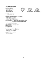
Page 1: ...SA450 Double sided Minifloppy Diskette Storage Drive m 1 r 1 AShugart ...

Page 2: ...Motor On 7 3 4 Track Accessing 7 3 4 1 Step Out 7 3 4 2 Step In 8 3 5 Side Selection 8 3 6 Read Operation 9 3 7 Write Operation 10 3 8 Sequence of Events 12 4 0 Electrical Interface 13 4 1 Signal Interface 14 4 1 1 Input Lines 14 4 1 1 1 Input Line Terminations 15 4 1 1 2 Drive Select 1 4 15 4 1 1 3 Motor On 15 4 1 1 4 Direction Select 16 4 1 1 5 Step 16 4 1 1 6 Write Gate 16 4 1 1 7 Write Data 16...

Page 3: ... Write Initiate Timing 11 8 Write Data Timing FM 11 9 General Control and Data Timing Requirements 12 10 Interface Connections 13 1 1 Interface Signal Driver Receiver 14 12 Step Timing 16 1 3 Write Data Timing 17 14 Index Timing SA1 54 Media 17 15 Index Sector Timing SA1 55 Media 18 16 Index Sector Timing SA1 57 Media 18 1 7 Read Data Timing FM 19 18 Interface Connectors Physical Locations 21 1 9 ...

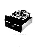
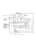
Page 4: ...FIGURE 1 SA450 DOUBLE SIDED MINIFLOPPY III ...

Page 5: ...to keep the door from closing on media DC drive motor with precision servo speed control and integral tachometer unique stepping motor actuator with direct drive spiral cam and ball bearing V groove positive detent same proprietary glass bonded ferrite ceramic read write head as used in Shugart s large floppy drives internal write protect circuitry activity light and solid die cast chassis Typical...

Page 6: ...ity 40 Track 35 Track Flux Density 40 Track 35 Track Track Density Media Requirements SA154 soft sectored SA155 16 sectors hard sectored SA157 10 sectors hard sectored Industry standard flexible diskette Oxide on 0 003 in 0 08mm Mylar 5 25 in 133 4mm square jacket Single Density Double Density FM MFM 250 000 500 000 218 750 437 500 125 000 250 000 109 375 218 750 3 125 6 250 163 840 327 680 143 36...

Page 7: ...imensions exclusive of front panel Width 5 75 in 146 1mm height 3 25 in 82 6mm Depth 8 0 in 203 2mm Nominal Weight 3 lbs 1 36KG Nominal Power Dissipation 1 1 5 Watts 40BTU Hr Continuous typical 7 3 Watts 25BTU HR Standby typical 1 2 4 Reliability Specifications MTBF 8000 POH under typical usage PM Not required MTTR 30 minutes Error Rates Soft Read Errors 1 per 1 9 bits read Hard Read Errors 1 per ...

Page 8: ...of a precision spiral cam This cam has a V groove with a ball bearing follower which is attached to the head carriage assembly Precise track location is accomplished as the cam is rotated in discrete increments by a stepping motor 2 5 Read Write Heads The proprietary heads are a single element ceramic read write head with straddle erase elements to provide erased areas between data tracks Thus nor...

Page 9: ......

Page 10: ... SELECT 4 LINES TRACK 00 INDEX SECTOR MOTOR ON SIDE SELECT SIDE SELECT CONTROL LOGIC WRITE HEADO WRITE HEAD 1 WRITE PROTECT N C WRITE PROTECT SWITCH ACTIVITY LIGHT NDEX SECTOR LED STEPPER MOTOR TRACK 00 COM TRACK 00 N O MOTOR ON STEPPER A MOTOR DRIVER MOTOR CONTROL TACHOMETER STEPPER B STEPPER C STEPPER D INDEX SECTOR LED INDEX SECTOR DETECTOR FIGURE 2 SA450 FUNCTIONAL DIAGRAM ...

Page 11: ...g this line to allow the motor to come up to speed before reading or writing can be accomplished The motor must be turned off by the host system by deactivating the MOTOR ON line This should be done if the drive has not received a new command within two 2 seconds 10 revolutions of diskette after com pleting the execution of a command This will insure maximum motor and media life 3 4 Track Accessin...

Page 12: ...STEP line must have the timing characteristics shown in Figure 3 3 5 Side Selection Head Selection is controlled via the I O signal line designated SIDE SELECT A plus logic level on the SIDE SELECT line selects the read write head on the side surface of the diskette A minus logic level selects the side 1 read write head When switching from one side to the other A 200 s delay is required after SIDE...

Page 13: ... order to guarantee that the read write heads position has stabilized prior to reading The timing of Read Data FM is shown in Figure 5 The encoding scheme of the recorded data can be either FM or MFM FM encoding rules specify a clock bit at the start of every bit cell Refer to Figure 6 MFM encoding rules allow clock bits to be omitted from some bit cells with the following prerequisites The clock ...

Page 14: ...MFM CODE COMPARISONS 3 7 Write Operation Writing data to the SA450 is accomplished by a Activating the DRIVE SELECT line b Selecting Head c Activating the WRITE GATE line d Pulsing the WRITE DATA line with the data to be written The timing relationships required to initiate a Write Data sequence are shown in Figure 7 These timing specifications are required in order to guarantee that the read writ...

Page 15: ...TE INITIATE TIMING y LJ LJ ur Lr Lr 200 ns MIN 2100 ns MAX 8 00jis 40 ns 400 iS 20 ns FIGURE 8 WRITE DATA TIMING FM Write data encoding can be FM or MFM The write data should be precompensated 100 ns on all tracks to counter the effects bit shift The direction of compensation required for any given bit in the data stream depends on the pattern it forms with nearby bits 11 ...

Page 16: ...RT PROT OUTPUT VALID INDEX SECTOR OUTPUT DIRECTION SELECT STEP WRITE GATE WRITE DATA VALID READ DATA SIDE SELECT 100 MS MIN 500 ns MAX 0 5 SEC MAX 500 ns MAX Vs MIN lS MIN 20 MS 15 MS 500 ns MIN 0 5 SEC MIN 200 s MIN 1 tsMIN 35 MS MIN 45 if 15 SS Sf 4 1f 8 Ms MAX if yinrnnnru 35 MS MIN 2 s MAX 0 5 SEC MAX inr if 8 iS MIN 100aiS MIN ni 200 s MIN ff FIGURE 9 GENERAL CONTROL AND DATA TIMING REQUIREME...

Page 17: ...SPARE SIGNAL LINE J1 2 i FLAT RIBBON OR TWISTED PAIR IN USE 4 3 5 7 9 i11 13 15 17 19 21 23 25 27 29 31 DRIVE SELECT 4 6 INDEX SECTOR 8 DRIVE SELECT 1 10 DRIVE SELECT 2 12 i DRIVE SELECT 3 14 MOTOR ON 16 1 DIRECTION SELECT 19 STEP 20 WRITE DATA 22 WRITE GATE 24 TRACK 00 4 26 AC GND TWISTED PAIR i WRITE PROTECT 28 READ DATA 30 SIDE SELECT 32 SPARE SIGNAL LINE 1 34 t 5VDC J2 4 3 2 FLOGIC GND 12VDC 1...

Page 18: ... affect all the drives in a daisy chain system The input signals to be multiplexed are 1 DIRECTION SELECT 2 STEP 3 WRITE DATA 4 WRITE GATE 5 SIDE SELECT The input signals which are intended to do the multiplexing are 1 DRIVE SELECT 1 2 DRIVE SELECT 2 3 DRIVE SELECT 3 4 DRIVE SELECT 4 The signals which are not multiplexed are IN USE and MOTOR ON The input lines have the following electrical specifi...

Page 19: ...orted and MS shorted DRIVE SELECT when ac tivated to a logical zero level will turn the motor on Since MX is shorted the I O lines are always enabled In a multiple drive system program shunt position MX open the four input lines DRIVE SELECT 1 DRIVE SELECT 2 DRIVE SELECT 3 and DRIVE SELECT 4 are provided so that the using system may select which drive oh the interface is to be used In this mode of...

Page 20: ...ro to logical one transition or the trailing edge of the signal pulse Any change in the DIRECTION SELECT line must be made at least 1 Ms before the trailing edge of the STEP pulse the DIRECTION SELECT logic level must be maintained Vs after trailing edge of STEP pulse Refer to Figure 12 for these timings V WRITE GATE DRIVE SELECT DIRECTION SELECT 500 ns MIN REVERSE STEP Vs MIN Vs MIN FIGURE 12 STE...

Page 21: ...d at track zero the outermost track and the access circuitry is driving current through phase A of the stepper motor This signal is at a logical one level or inactive state when the drive s read write heads are not at track zero When the drive s read write heads are at track zero and an additional step out pulse is issued to the drive a mechanical stop will keep the read write heads at track zero ...

Page 22: ...s the raw data clock and data together as detected by the drive electronics Normally this signal is a logical one level and becomes a logical zero level for the active state Refer to Figure 17 for the timing and bit shift tolerance within normal media variations 4 1 2 4 Write Protect This interface signal is provided by the drive to give the user an indication when a Write Protected Diskette is in...

Page 23: ...host system AC or frame ground Failure to do so may result in drive noise susceptibility The 1 2V current is composed of 3 components Diskette Drive Motor Current Read Write stepper functions on the PCB and Write Erase Current In the multiplex mode the drive motor is turned off when the Drive is deselected but can be turned on by the MOTOR ON interface line Each of these functions has the followin...

Page 24: ......

Page 25: ...P N 583717 5 Frame Ground Amp P N 61664 1 J2 Amp P N 350211 1 Frame Connector Amp P N 60972 1 P2 Connector Amp P N 1 480424 0 FIGURE 18 INTERFACE CONNECTORS PHYSICAL LOCATIONS 5 1 J1 P1 Connector Connection to J1 is through a 34 pin PCB edge connector The dimensions for this connector are shown in Figure 19 The pins are numbered 1 through 34 with the even numbered pins on the component side of the...

Page 26: ...Wire used should be 18 AWG Figure 20 illustrates J2 connector as seen on the drive PCB from non component side FIGURE 20 J2 CONNECTOR 5 3 Frame Grounding The SA450 must be frame grounded to the host system to insure proper operation If the frame of the drive is not fastened directly to the frame of the host system with a good AC ground a wire from the system AC frame ground must be connected to th...

Page 27: ...ing mounted upright 2 Front Loading mounted vertical with door opening left or right mounted horizontal with PCB up DO NOT HORIZONTAL MOUNT WITH PCB DOWN Mounting Holes 4 on bottom 2 on each side 6 32 x 25 DP MIN 8x 63 29 73 04 10 CO CJ1 19 02 48 05 8 25 max 20 96 5 675 02 14 41 05 1 905 060 4 84 15 _ 3 12 04 8x 7 92 10 MINI PCB 06 01 15 02 834 050 4 X K 2 12 13 i ii cn cn fc J J CD en 1 io o o S ...

Page 28: ...pondingly the most significant byte of data is transferred to the disk first and the least significant byte is transferred last When data is being read back from the drive bit cell of each byte will be transferred first with bit cell 7 last As with reading the most significant byte will be transferred first from the drive to the user Figure 22 illustrates the relationship of the bits within a byte...

Page 29: ...RECORDS 10 RECORDS 5 RECORDS 2 RECORDS 1 RECORDS UPDATE WRITE 00 SUSER I 1 DATA HJ FF FF 128 128 256 512 1024 2048 GAP 4 FF 11 85 26 101 19 69 70 54 499 5 1032 NOTES 1 Track Number Head Number Sector Number Sector Length 2 IBM or Equivalent CRC Generator 3 FB for Data or F8 for Deleted Data FIGURE 24 RECOMMENDED SOFT SECTOR SINGLE DENSITY FM EVEN BOUNDARIES PHYSICAL INDEX 1 NUMBER OF BYTES HEX BYT...

Page 30: ...nc is a fixed number of bytes for Separator synchrohiztion prior to the AM Includes a minimum of two bytes plus worst case separator sync up requirements Pre Data Address Mark MFM Three bytes of A1 with unique clock bits not written per the encode rules Data Address Mark FM is a unique byte to identify the Data Field and it is not written per the encode rules Data Address Mark MFM is one byte of F...

Page 31: ...RECORDS 128 36 10 RECORDS FF 256 25 AA MFM OB B HEX BYTE AA NUMBER OF BYTES 16 6 1 4 2 16 RECORDS 256 101 10 RECORDS 512 79 UPDATE WRITE I NOTES 1 Track Number Head Number Record Number Record Length 2 User Data 3 Generated by CRC Generator IBM or Equivalent FIGURE 26 RECOMMENDED HARD SECTOR FM AND MFM FORMATS 27 ...

Page 32: ...c tape apply These precautionary procedures are as follows 1 Return the diskette to its storage envelope whenever it is removed from drive 2 Do not bend or fold the diskette 3 Store diskettes not for immediate use in their box 4 Keep diskettes away from magnetic fields and from ferromagnetic materials which might become magnetized Strong magnetic fields can distort recorded data on the disk 5 Repl...

Page 33: ... a Shugart Copyright Shugart 475 Oakmead Parkway Sunnyvale California 94086 Telephone 408 733 0100 TWX 910 339 9355 SHUGART SUVL 39013 1 10 80 PRINTED IN U S A ...

Reviews: