background image

SERVICE MANUAL

8M29B CHASSIS

Description:

MODEL.

Engineering Dept:

Artwork By:

Checked By:

Approved By:

Brand Name:

JOB NO.

Date:

Date:

Date:

SERVICE MANUAL 8M29B

2011-5-23

SKYWORTH

SIZE:A5

Design and specifications are subject to change without prior notice.

(Only Referrence)

Summary of Contents for 8M29B

Page 1: ...scription MODEL Engineering Dept Artwork By Checked By Approved By Brand Name JOB NO Date Date Date SERVICE MANUAL 8M29B 2011 5 23 SKYWORTH SIZE A5 Design and specifications are subject to change without prior notice Only Referrence ...

Page 2: ...Content 2 2 Technical Specification 3 14 8M29 Block Diagram 15 List of key parts 16 IC BLOCK Diagram 17 31 MAIN PCB TOP 32 MAIN PCB BOT 33 Circuit Diagrams 34 42 ...

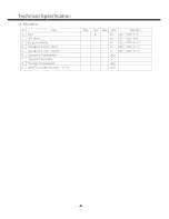
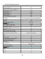
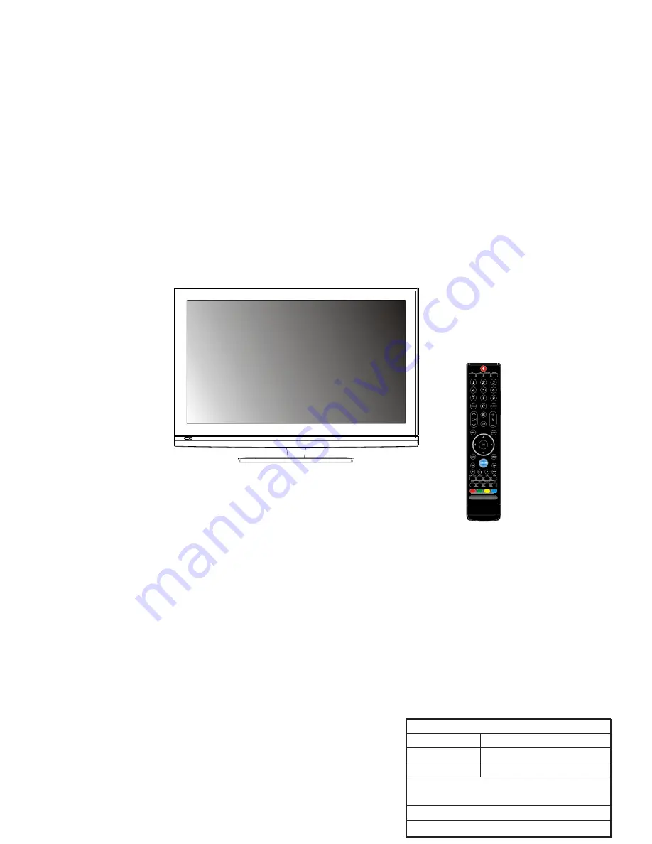
Page 3: ... 3 LCD 8M29B chassis ...

Page 4: ...105 140 For 32LED For 42LED 4 4 5 Base on different order FOR 32LED FOR 42LED 93 400 95 97 93 95 97 450 ...

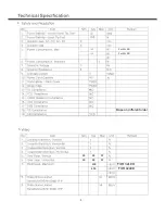
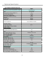
Page 5: ...For 42LED For 42LED 5 8 8 10 15 9800 12500 12500 266 276 9800 280 290 6500 313 329 ...

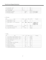
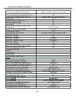
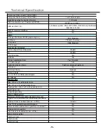
Page 6: ...40 40 3 2 1 4 2 50 0 5 80 40 12000 6 24 6 ...
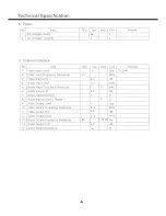
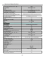
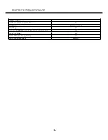
Page 7: ...1080 1920 uv uv 40 YES 8 6 46 46 NO NO Standard English Standard 20 Middle 7 For 42LED For 42LED Base on different order No Low in some status ...

Page 8: ... 8 4 ...

Page 9: ...e Finish Regional requirement Homologation Gostandard CE MPTT CB CB RoHS Yes Power supply 100 240V AC 10 100 240V AC 20 10 Power consumption working Annual Power consumption standby 1W Power plug VDE UL BS UCIEE 2pins Picture display Screen size diagonale inch 32 42 46 Aspect ratio 16 9 4 3 15 9 16 9 1st panel supplier panel suppliers LG 1st panel supplier panel reference Panel Display Type MVA PV...

Page 10: ... Zoom type Auto by SCART Pin8 and WSS Yes Picture Auto adjustment PC mode Yes 3D Panel Type PR SG 3D Mode 3D To 2D Y N 2D To 3D Y N Left Right Swap For PR Panel Sound Sound type Mono AV stereo Stereo stereo Music Power Watt RMS Power Watt 2 x 8W Tone control Bass Treble Graphic Equalizer Bass Treble Special sound effect AVL WIDE Pseudo AVL Suround system Dolby VD SRS BBE Built in Surround Sound co...

Page 11: ...nish Portuguese French OSD Positioning No OSD Transparency Adjust No OSD Timeout Adjust No Customer Brand name LOGO Yes IB languages English ATV Program Numbers example 99 3AV input 99 7AV DTV Program Numbers 600 Program edit naming sorting skip swap Naming Skip Swap Auto Naming Auto Sorting No TV Guide DTV EPG EPG next Seven day Favorite program Yes Number of buttons on cabinet Power Vol Pr Menu ...

Page 12: ...ctors Rear RF Input Antenna Air Cable 2in1 Air Cable Scart CVBS in out RGB S VIDEO No CINCH video in out AV1 No CINCH audio in out No volumpe control on Audio out can be jack 3 5mm No S video in No Component Video Input YCrCb YPrPb No Component Audio Input YCrCb YPrPb No VGA in Audio L R in Jack audio in 3 5mm VGA dia 3 5mm for audio in HDMI 2 DVI No Audio input for DVI No CINCH subwoofer out Coax...

Page 13: ...ration Card Yes English AC Cable Length 1 8m Audio Cord Jack 3 5mm Yes For component audio in VGA Cord No Wallmount frame Optional Antenna Cable No 6 in 1 YPbPr CVBS cable adapter No 3D Glasses No General Data Size W x H x D with stand in mm Size W x H x D without stand in mm Package Size W x H x D without stand in mm Net Weight in kg Gross Weight in Kg Design Mechanical Wallmount VESA compatible ...

Page 14: ...n stand number of colors on carton box 2 Brand logo Customer Inlet Other logo No External AC DC Power with DC power cord yes No No Handle yes No No Detachable speaker yes No No Rating Label langages English 14 ...

Page 15: ...ar Terminals HDMI2 HDMI3 PC PC Audio S PDIF HDMI1 Uplayer2 IF SAW P S PIXELWORKS 3D Processor Motion Engine PA131DG Uplayer1 MSD309PX LF SB DVB T IF Demo Build in MPEG1 2 4 H 264 Decoder JPEG MP3 Decoder 3D Comb filter Video Decoder DVB T ATV Demo d KEY PAD IR Receiver Ambient Sensor IF ATV ATV DTV Tuner Optional 15 ...

Page 16: ...4401 4900 744015 0X00 U3 MP1482DS 476A M14820 0080 U5 MP1482DS 476A M14820 0080 8 MP1482DS 476A M14820 0080 8 MP1482DS 476A M14820 0080 U9 W9751G6JB 25 4737 W97511 0840 U15 W9751G6JB 25 4737 W97511 0840 U24 EN25F32 100HIP 471R N25321 0080 U55 TC90517FG 4701 T90510 0640 U37 AS1117L 3 3 47B6 A11170 03 U38 AS1117L 3 3 47B6 A11170 03 N1 AS1117L 3 3 47B6 A11170 03 N2 AS1117L 1 2 47B6 A11175 0300 U54 TP...

Page 17: ...5 2 O T 0 2 2 O T Pin Configurations AS1117L 3 3 INPUT OUTPUT ADJ GND VOUT INPUT OUTPUT ADJ GND VOUT INPUT OUTPUT ADJ GND VOUT 1 2 3 1 2 3 1 2 3 U Package ADJ GND OUTPUT INPUT VOUT S Package TO 263 R Package INPUT OUTPUT ADJ GND SOT 89 1 2 3 1 2 3 VOUT ...

Page 18: ...t is given by Name Description FB Feedback pin EN Power off pin HΚnormal operation Step down LΚStep down operation stopped All circuits deactivated OCSET Add an external resistor to set max switch output current VCC IC power supply pin SW Switch pin Connect external inductor diode here Top View 1 2 3 4 8 7 6 5 FB Ocset SOP 8L AX3113 Vcc EN Vss Vss SW SW VSS GND pin ...

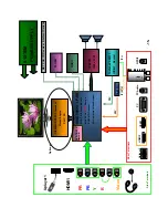
Page 19: ...IC Block Diagram 19 LM4558 MP1482DS BS IN SW GND SS EN COMP FB 1 2 3 4 8 7 6 5 TOP VIEW ...

Page 20: ...IC Block Diagram 20 MST6M20S LF ...

Page 21: ... 19 18 17 16 15 14 13 PVCCL SD PVCCL MUTE LIN RIN BYPASS AGND AGND PVCCR VCLAMP PVCCR PGNDL PGNDL LOUT BSL AVCC AVCC GAIN0 GAIN1 BSR ROUT PGNDR PGNDR PWP TSSOP PACKAGE TOP VIEW PIN CONFIGURATION SOIC 150 MIL 208 MIL PAD CONFIGURATION WSON 6X5 MM PIN CONFIGURATION PDIP 300 MIL ...

Page 22: ...IC Block Diagram 22 EN25F32 Figure 1 CONNECTION DIAGRAMS 8 LEAD SOP DIP 8 CONTACT VDFN 16 LEAD SOP ...

Page 23: ...IC Block Diagram 23 EN25F32 Figure 2 BLOCK DIAGRAM ...

Page 24: ... program or status register cycle is in progress When CS is brought low the device will be selected power consumption will increase to active levels and instructions can be written to and data read from the device After power up CS must transition from high to low before a new instruction will be accepted Hold HOLD The HOLD pin allows the device to be paused while it is actively selected When HOLD...

Page 25: ... 2 C control Filter AGC ISIC unguarded preecho postecho suppression FFT Control Adaptive interpolation filter Equalization CSI reliability detection CVI CW interference detection AGC control output Tuner I 2 C Clock PLL Viterbi decoding Memory Frequency deinterleaving RS decoding Error detection Output control Layer isolation TMCC demodulation Interpolation phase correction Synchroni zation Demapp...

Page 26: ...IC Block Diagram 26 TC90517FG Toshiba products specification Tentative CONFIDENTIAL 3 Pin Assignment Top view ...

Page 27: ...o crystal The amplitude p p is 0 5 V to PLLVDD when an external reference clock is input 20 PLLVDD Clock PLL power supply Connects to analog 2 5 V typ 21 FIL O PLL filter output Connects to AGND via 1500 pF 22 AD_AVDD ADC analog power supply Connects to analog 2 5 V typ 23 AD_AVSS ADC analog GND Connects to AGND 24 AD_VREFP ADC reference voltage output 1 75 V typ Connects to AGND via PC 25 AD_VREF...

Page 28: ...g output Open fixed to L when not used 56 VDDC Digital 1 2 V power supply Connects to digital 1 2 V typ 57 VSS Digital GND Connects to DGND 58 PBVAL O TS valid flag output Open fixed to L when not used 59 SBYTE O TS synchronization byte flag output Open fixed to L when not used 60 SRDT O Serial TS data output 61 SRCK O TS serial clock output 62 VSS Digital GND Connects to DGND 63 VDDC Digital 1 2 ...

Page 29: ...S V D D Q V D D Q D Q 7 V D D O D T V D D D Q 14 V D D Q D Q 12 N C V D D L N C V S S Q D Q 9 V S S Q A 3 C K E B A 0 B A 1 W E D Q 3 LD M V S S D Q 11 V D D Q V S S U D M V D D D Q 6 V D D Q D Q 4 V S S V D D A 12 N C N C N C A 11 A 8 A 9 A 7 A 5 A 1 A 10 A P V S S V R E F D Q 1 V S S Q V D D Q V S S Q N C V S S Q LD Q S V S S Q D Q 10 D Q 15 D Q 13 V D D Q V D D Q D Q 5 V D D V S S M N P R V S S...

Page 30: ... used when differential data strobe mode is enabled via the control bit at EMR 1 A10 EMRS command L8 Chip Select All commands are masked when is registered HIGH provides for external bank selection on systems with multiple ranks is considered part of the command code K7 L7 K3 RAS CAS Command Inputs RAS CAS and along with define the command being entered B3 F3 UDM LDM Input Data Mask DM is an input...

Page 31: ...UMN DECODER SENSE AMPLIFIER CELL ARRAY BANK 2 COLUMN DECODER SENSE AMPLIFIER CELL ARRAY BANK 0 COLUMN DECODER SENSE AMPLIFIER CELL ARRAY BANK 3 DATA CONTROL CIRCUIT DQ BUFFER COLUMN DECODER SENSE AMPLIFIER CELL ARRAY BANK 1 NOTE The cell array configuration is 8192 1024 16 A0 A9 A11 A12 BA1 BA0 CS RAS CAS WE CLK CLK PREFETCH REGISTER ODT CONTROL DQ0 DQ15 LDQS LDQS UDQS UDQS LDM UDM ODT ...

Page 32: ...MAIN PCB TOP 32 ...

Page 33: ...MAIN PCB BOT 33 ...

Page 34: ... 2 3 U3 MPS1482 U3 MPS1482 IN 2 BS 1 GND 4 FB 5 COMP 6 EN 7 SS 8 SW 3 C442 0 1u C442 0 1u C104 10n C104 10n ADJ OUT IN U37 AMS1117 3 3V ADJ OUT IN U37 AMS1117 3 3V 3 2 1 4 C481 3 3nF C481 3 3nF C427 0 1u C427 0 1u C394 NC 0 1u C394 NC 0 1u TP6 TP6 1 R25 0 R25 0 R43 5 6K R43 5 6K TP22 TP22 1 C32 NC 0 1uF C32 NC 0 1uF R24 1K R24 1K CA18 470uF 16V CA18 470uF 16V C3 10nF C3 10nF C439 0 1u C439 0 1u U5...

Page 35: ...L10 AVDD_DVI F9 AVDD_DVI F10 AVDD_DVI G9 AVDD_DMPLL G10 AVDD3P3_ADC H9 AVDD3P3_ADC H10 GND V7 GND W7 GND V8 GND W8 GND V9 GND W9 GND J10 GND K10 GND M10 GND N10 GND P10 GND R10 GND T10 GND U10 GND V10 GND W10 GND D11 GND G11 GND H11 GND J11 GND K11 GND L11 GND M11 GND N11 GND P11 GND R11 GND T11 GND U11 GND V11 GND W11 GND D12 GND E12 GND F12 GND G12 GND H12 GND J12 GND K12 GND L12 GND M12 GND N12...

Page 36: ... 1 8 6 4 2 RP19 75RX4 R107 10k R107 10k 7 5 3 1 8 6 4 2 RP21 22RX4 7 5 3 1 8 6 4 2 RP21 22RX4 7 5 3 1 8 6 4 2 RP1 22RX4 7 5 3 1 8 6 4 2 RP1 22RX4 7 5 3 1 8 6 4 2 RP17 75RX4 7 5 3 1 8 6 4 2 RP17 75RX4 7 5 3 1 8 6 4 2 RP6 75RX4 7 5 3 1 8 6 4 2 RP6 75RX4 R378 100R R378 100R 7 5 3 1 8 6 4 2 RP18 75RX4 7 5 3 1 8 6 4 2 RP18 75RX4 A B C D E F G H J K L M N P R 1 2 3 7 8 9 Vdd NC Vss DQ14 VssQ UDM VddQ DQ...

Page 37: ...r RFAGC㛮ᬒ㕂 DVB T TUNER TUNER POWER 䴴䖥tunerᬒ㕂 Q604 3906 Q604 3906 1 3 2 C89 0 1u C89 0 1u C474 0 1u C474 0 1u R429 NC 390R R429 NC 390R U10 VA1P1BF8401 U10 VA1P1BF8401 Body 15 NC 3 AS 4 SDA 6 SCL 5 IFD_OUT2 11 IF_AGC 9 IFD_OUT1 10 Body 12 Body 14 Body 13 RFAGC_M 1 NC 2 VCC_5V 7 IFA_OUT 8 R422 100K R422 100K R456 22R R456 22R Q403 3904 Q403 3904 1 2 3 U11 VA1P1BF8402 U11 VA1P1BF8402 Body 15 NC 3 AS ...

Page 38: ...02 Q416 3904 Q416 3904 1 2 3 DD81 NC ESD 0402 DD81 NC ESD 0402 R135 10R R135 10R R149 10R R149 10R Q412 3904 Q412 3904 1 2 3 R140 10R R140 10R R146 10R R146 10R DD86 NC ESD 0402 DD86 NC ESD 0402 R161 1K R161 1K R354 NC 10K R354 NC 10K DD55 ESD 0402 DD55 ESD 0402 DD97 NC ESD 0402 DD97 NC ESD 0402 R158 10K R158 10K R183 10K R183 10K R160 10R R160 10R DD68 ESD 0402 DD68 ESD 0402 DD82 NC ESD 0402 DD82...

Page 39: ...43 1n C43 1n C101 47n C101 47n R241 75R R241 75R P5 PHONEJACK STEREO SW 180d P5 PHONEJACK STEREO SW 180d 1 2 3 R214 10K R214 10K R63 75R R63 75R C96 47n C96 47n P15A P15A 1 1 2 2 3 3 4 4 6 6 5 5 7 7 R113 100R R113 100R C126 2 2u C126 2 2u R346 NC 100R R346 NC 100R R84 33R R84 33R R254 75R R254 75R R66 10K R66 10K R326 12K R326 12K R104 68R R104 68R R156 0R R156 0R C97 1n C97 1n C67 200p C67 200p P...

Page 40: ...ay December 10 2010 Title Size Document Number Rev Date Sheet of 8 10 0 1 USB A 8 10 Friday December 10 2010 2pF 2pF 2pF 2pF close to USB connector 2010 3 3 R189 4 7K R189 4 7K R297 0R R297 0R R282 0R R282 0R CA110 100uF 16V CA110 100uF 16V P9 USB_A P9 USB_A 1 1 2 2 3 3 4 4 5 5 6 6 Q434 3904 Q434 3904 1 2 3 R61 4 7K R61 4 7K R287 0R R287 0R R298 0R R298 0R P9A USB_A P9A USB_A 1 1 2 2 3 3 4 4 5 5 6...

Page 41: ...12K C254 4 7u C254 4 7u R438 470 R438 470 U45A TL062 U45A TL062 3 2 1 8 4 R294 24K R294 24K L1 CON2_1 L1 CON2_1 2 1 3 4 5 6 R369 10K R369 10K C267 1uF C267 1uF R365 1 5K R365 1 5K R280 10K R280 10K R335 10K R335 10K C264 1uF C264 1uF Q35 A03401 Q35 A03401 1 3 2 R278 100R R278 100R R361 10K R361 10K R398 330R R398 330R H15 TPAD H15 TPAD 1 R367 10K R367 10K CA83 470uF 16V CA83 470uF 16V CA55 220uF 3...

Page 42: ... C881 1500pF R533 NC 1K R533 NC 1K R535 1K R535 1K L408 FB0603 L408 FB0603 L410 FB220 300mA L410 FB220 300mA C886 1u C886 1u 7 5 3 1 8 6 4 2 RP62 33RX4 7 5 3 1 8 6 4 2 RP62 33RX4 C863 0 1u C863 0 1u C883 NC 10p C883 NC 10p R530 1K R530 1K R525 10K R525 10K C855 1u C855 1u C856 0 1u C856 0 1u C861 0 1u C861 0 1u R510 100R R510 100R C897 100uF 16V C897 100uF 16V C894 100uF 16V C894 100uF 16V R513 10...

Page 43: ...3 3 3UH R47 101 2W R47 101 2W F2 FUSE T1A 250VAC F2 FUSE T1A 250VAC U9 PC817C U9 PC817C 1 2 3 4 C49 4 7U 50V C49 4 7U 50V LF1 ET24E LF1 ET24E 1 2 3 4 J18 J18 D32 2 2M 1 2W D32 2 2M 1 2W L3 5uH L3 5uH CX1 224 275VAC CX1 224 275VAC R21A 2M2 1 4W R21A 2M2 1 4W R15 3 3K 2W R15 3 3K 2W J23 J23 C27 224 C27 224 C23 2200uF 10V C23 2200uF 10V BD1 KBJ606J BD1 KBJ606J 2 1 3 4 R67 2K 1 6W R67 2K 1 6W CN2 PIN1...

Page 44: ... Rev Date Sheet of Doc RevCode 5800 P32ALB W010 Custom 2 3 Tuesday September 20 2011 C46 474 C46 474 U1 OB6572AP U1 OB6572AP GND 1 ICOMP 2 ISENSE 3 FRE 4 VCOMP 5 VSENSE 6 VCC 7 Gate 8 C48 104 C48 104 J23 J23 R9 2 2M 1 4W R9 2 2M 1 4W R13 471 1 6W R13 471 1 6W C40 104 C40 104 C44 472 C44 472 R36 33R 1 6W R36 33R 1 6W R99 20K 1 6W R99 20K 1 6W C41 10U 35V C41 10U 35V R100 33R 1 6W R100 33R 1 6W R8 2...

Page 45: ...148 J8 J8 CA15 104 CA15 104 CA17 474 CA17 474 RA23 10R 1 6W RA23 10R 1 6W J25 J25 CA20 105 450V CA20 105 450V RA28 22R 1 6W RA28 22R 1 6W QA5 T01N60 QA5 T01N60 2 1 3 U6 OB3309 U6 OB3309 DRC 4 BF DMOD 5 POL 6 VDD 7 GATE1 8 GATE2 9 GND 10 VS 11 PRT 12 CS 13 CMP 14 STIME 15 ENA 1 RT 3 RI 2 DIM 16 RA16 1K 1 6W RA16 1K 1 6W RA17 121R 2W RA17 121R 2W J2 J2 QA9 2N2907 QA9 2N2907 1 3 2 CA5 472 1KV CA5 472...

Reviews: