background image

CDP-C591/CE235/CE335

US Model

CDP-C591/CE235/CE335

Canadian Model

AEP Model

UK Model

E Model

Australian Model

CDP-CE235/CE335

SERVICE MANUAL

COMPACT DISC PLAYER

MICROFILM

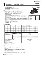
SPECIFICATIONS

Model Name Using Similar Mechanism

NEW

CD Mechanism Type

CDM27-5BD32A

Base Unit Type

BU-5BD32A

Optical Pick-up Type

KSS-213BA/F-NP

Compact Disc Player

Laser

Semiconductor laser (

λ

 = 780 nm)

Emission duration: continuous

Laser output

Max 44.6 µW*
* This output is the value measured at a distance of

200 mm from the objective lens surface on the
Optical Pick-up block with 7 mm aperture.

Frequency response 2 Hz to 20 kHz ± 0.5 dB
Signal-to-noise ratio More than 102 dB
Dynamic range

More than 98 dB

Harmonic distortion Less than 0.0045%

Output

Jack

Maximum

Load

type

output

impedance

level

LINE OUT

Phono

2V

Over 10 k

jacks

(at 50 k

)

DIGITAL OUT

Optical

–18 dBm

Wave length:

(OPTICAL)

output

660 nm

connector

General

Power requirements

Where purchased

Power requirements

USA and Canada

120V AC, 60 Hz

Europe and some Asian countries

220V – 230V AC, 50/60 Hz

Other countries

110V – 120V AC or 220V –
240V AC, adjustable, 50/60 Hz

Power consumption

14 W

Dimensions (approx.) 430 

×

 120 

×

 385 mm

(w/h/d)

(17 

×

 4 

3

/

4


×

 15 

1

/

4

 in.) incl. projecting parts

Mass (approx.)

5.4 kg (11 lbs 15 oz)

Supplied accessories

Audio cord (2 phono plugs–2 phono plugs) (1)
Remote commander (remote) (1) (CDP-CE335 only)
R6 (size AA) batteries (2) (CDP-CE335 only)

Design and specifications are subject to change without notice.

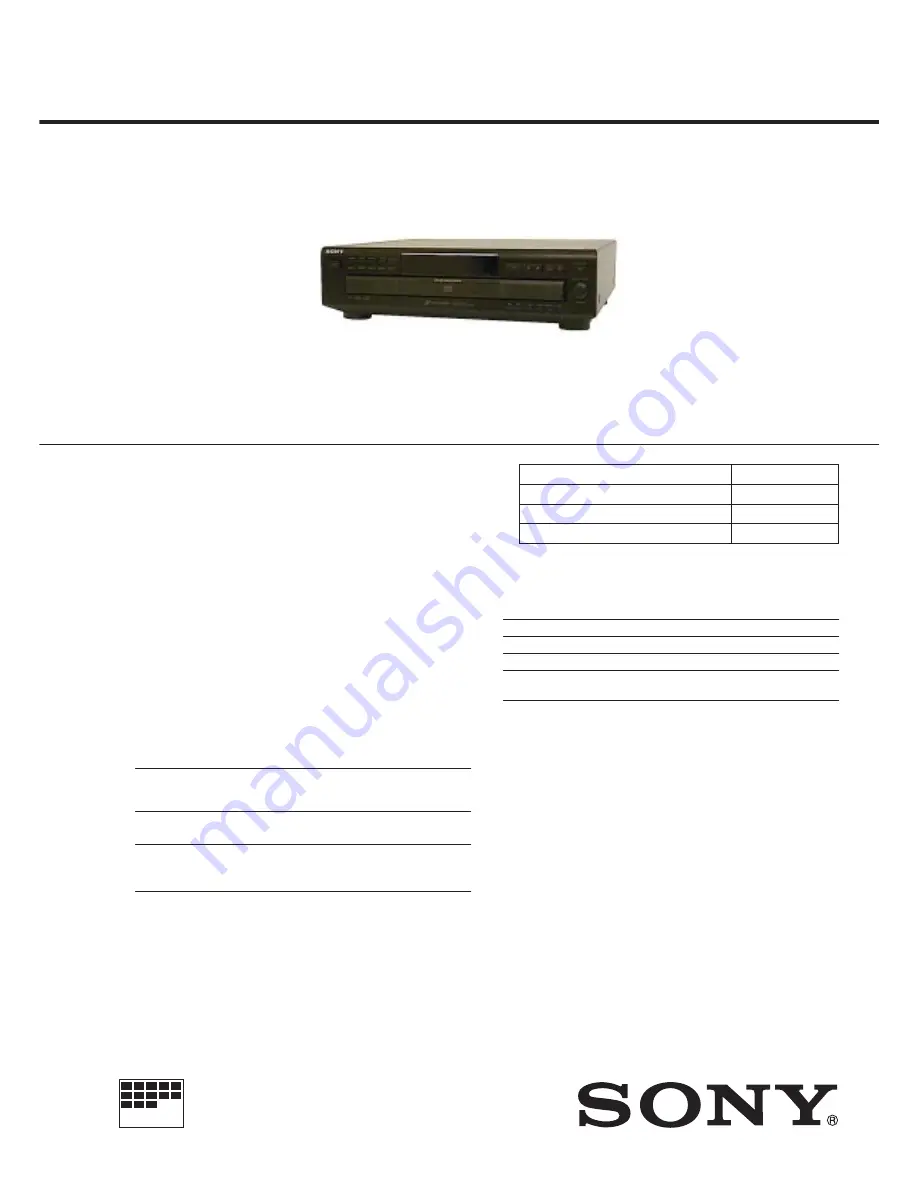
Photo : CDP-CE235

Summary of Contents for CDP-C591

Page 1: ...ratio More than 102 dB Dynamic range More than 98 dB Harmonic distortion Less than 0 0045 Output Jack Maximum Load type output impedance level LINE OUT Phono 2V Over 10 kΩ jacks at 50 kΩ DIGITAL OUT Optical 18 dBm Wave length OPTICAL output 660 nm connector General Power requirements Where purchased Power requirements USA and Canada 120V AC 60 Hz Europe and some Asian countries 220V 230V AC 50 60 ...

Page 2: ...RKING is located on the rear exterior CAUTION Use of controls or adjustments or performance of procedures other than those specified herein may result in hazardous radiation exposure 1 GENERAL 5 2 DISASSEMBLY 2 1 Case Bottom Plate and Front Panel 6 2 2 Back Panel and Disc Table 6 2 3 Optical Pick up Block Assembly 7 2 4 Bracket Gear Assembly 7 3 TEST MODE 8 4 ELECTRICAL BLOCK CHECKING 9 5 DIAGRAMS...

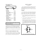
Page 3: ...meter The Data Precision 245 digital multimeter is suitable for this job 3 Measuring the voltage drop across a resistor by means of a VOM or battery operatedAC voltmeter The limit indication is 0 75 V so analog meters must have an accurate low voltage scale The Simpson 250 and Sanwa SH 63Trd are examples of a passive VOM that is suitable Nearly all battery operated digital multimeters that have a ...

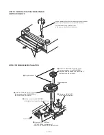
Page 4: ... out of the ENCODER to the right when viewed from the front view 3 Install the MAIN GEAR while aligning the protrusion of the MAIN GEAR to the cut off of the ENCODER 6 Stopper washer 5 5 Rotate the MAIN GEAR until the portion that has no gears of the MAIN GEAR is aligned with the shaft of the GEAR REV Then insert the GEAR REV Projected portion SHAFT 1 Rotate the GEAR U D to the arrow A direction 4...

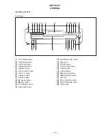
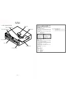
Page 5: ...6 DISC CHECK button 7 DISC 1 5 button 8 Display window 9 play button º P pause button p stop button EX CHANGE button DISC SKIP button 6 OPEN CLOSE button AMS knob FADER button MUSIC SCAN button CLEAR button ª CHECK button º forward button 0 backward button Disc tray PEAK SEARCH button EDIT TIME FADE button TIME button 1 2 3 4 5 6 7 8 9 0 º ª ...

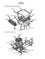
Page 6: ... screws M3 8 3 Two screws BV3 8 1 Two screws M3 8 0 Two screws BVTT3 8 Front panel 4 Case 8 Flat type wire 35 core MAIN board to CN402 9 Flat type wire 9 core MAIN board to CN402 7 Screw BVTP 3 8 Screw BVTP 3 8 9 Screw BVTP 3 8 5 Screw BVTP 3 8 6 Bracket guide B1 Bracket guide B1 0 Bracket guide F1 8 Bracket guide F1 4 Flat type wire 6 core MAIN board to CN404 1 Connector 3 Back panel Disc table B...

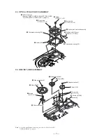
Page 7: ...mpression spring BU 1 Pull out the tray Refer to HOW TO OPEN THE DISC TRAY WHEN POWER SWITCH TURNS OFF on page 4 6 Holder BU 8 Compression spring BU 9 Optical pick up block assembly 2 Flat type wire 16 core BD board to CN101 3 Screw PTPWH 3 12 6 Rotary encoder 4 Gear MAIN 2 Gear REV 8 Gear U D 0 Bracket GEAR assembly 3 Stopper washer 5 1 Stopper washer 5 7 Stopper washer 5 5 Screws BVTP 3 8 9 Five...

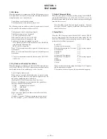
Page 8: ...r of the keys that have been pressed appear on the left and the key number appears on the right Pushing the JOG key is counted as one of the keys However the following keys are treated as the special keys that show the different operations STOP All display turn on check PLAY Grid check PAUSE Segment check JOG Calendar check When receiving a signal from remote controller the display appears Number ...

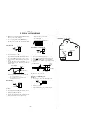
Page 9: ...ecks S Curve Check Procedure 1 Connect oscilloscope to TP FE 2 Connect between TP FE1 and TP VC by lead wire 3 Connect between TP AGCCON and TP GND by lead wire 4 Turn Power switch on 5 Load a disc YEDS 18 and actuate the focus search In consequence of open and close the disc tray actuate the focus search 6 Confirm that the oscilloscope waveform S curve is symmetrical betweenA and B And confirm pe...

Page 10: ... respect to ground under no signal detuned conditions Voltages are taken with aVOM Input impedance 10 MΩ Voltage variations may be noted due to normal produc tion tolerances Waveforms are taken with a oscilloscope Voltage variations may be noted due to normal produc tion tolerances Circled numbers refer to waveforms Signal path J CD c CD DIGITAL Abbreviation CND Canadian AED North European AUS Aur...

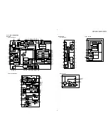
Page 11: ... MIRR DFCT FOK DETECTOR DIGITAL CLV SUBCODE PROCESSOR SERVO INTERFACE SERVO DSP FOCUS SERVO TRACKING SERVO SLED SERVO PWM GENERATOR FOCUS PWM GENERATOR TRACKING PWM GENERATOR SLED PWM GENERATOR 16K RAM ERROR CORRECTOR INTERNAL BUS A D CONVERTER OPERATIONAL AMPLIFIER ANALOG SWITCH 11 12 10 VC VC VC VC VC VC VC VCC VCC RF SUMMING AMP RF_EQ_AMP ERROR AMP FOCUS TRACKING ERROR AMP VC BUFFER VCC VCC VC ...

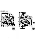
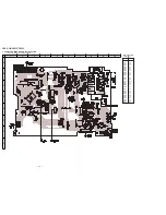
Page 12: ...ED WIRING BOARD BD SECTION See page 10 for Circuit Board Location Page 14 E 16 16 GND TE1 FE1 RF VC FE TE AGCCON PLCK Ref No Location IC101 C 2 IC102 B 1 IC103 B 1 Semiconductor Location Ref No Location Q101 C 3 Semiconductor Location ...

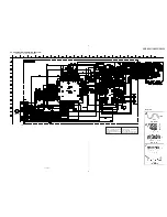
Page 13: ...r IC Block Diagrams Waveform The components identified by mark or dotted line with mark are critical for safety Replace only with part number specified Les composants identifiés par une marque sont critiques pour la sécurité Ne les remplacer que par une pièce portant le numéro spécifié ...

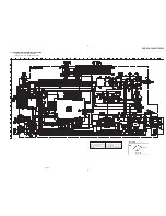
Page 14: ... 6 7 8 9 10 12 16 16 16 16 16 Ref No Location D302 F 7 D401 G 9 D501 G 9 D601 C 7 D602 B 7 D603 B 7 D604 B 7 D605 C 7 D606 C 7 D608 D 7 D609 D 6 IC302 D 2 IC304 D 5 IC371 G 10 IC401 E 7 IC601 C 6 IC602 C 6 IC603 C 7 Q201 E 4 Q402 E 8 Q404 C 2 Q405 F 9 Q406 E 8 Q502 F 8 Q503 G 9 Q505 F 9 Q506 E 8 Q601 C 7 Semiconductor Location ...

Page 15: ...for IC Pin Function IC302 17 17 13 17 17 The components identified by mark or dotted line with mark are critical for safety Replace only with part number specified Les composants identifiés par une marque sont critiques pour la sécurité Ne les remplacer que par une pièce portant le numéro spécifié Waveform ...

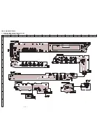
Page 16: ...CDP C591 CE235 CE335 16 5 7 PRINTED WIRING BOARD DISPLAY SECTION See page 10 for Circuit Board Location 1 2 A B C D E F G H I 3 4 5 6 7 8 9 10 11 12 14 14 14 14 ...

Page 17: ...CDP C591 CE235 CE335 17 5 8 SCHEMATIC DIAGRAM DISPLAY SECTION 15 15 15 15 ...

Page 18: ...nd Not used Open FL display tube segmant output 1 FL display tube segmant output 2 FL display tube segmant output 3 I O O O O O O O O O O O O O O O O O O O O O O O O O O O O O I O I I I Pin Name P4 P5 P6 P7 P8 P9 P10 P11 P12 P13 P14 P15 P16 P17 P18 P19 P20 NC G1 G2 G3 G4 G5 G6 G7 G8 VG VDD NC NC NC AFADJ BUS OUT DSENS SENS SCOR Pin No 41 42 43 44 45 46 47 48 49 50 51 52 53 54 55 56 57 58 to 62 63 ...

Page 19: ...ro spécifié 6 1 FRONT PANEL AND CASE SECTION 8 16 15 2 3 6 7 1 9 1 1 not supplied 21 17 17 17 17 17 22 21 21 20 7 2 1 not supplied 1 19 18 14 11 10 13 12 5 4 1 4 997 437 11 PANEL LOADING 2 4 987 779 01 WINDOW FL CE235 C591 2 4 987 779 11 WINDOW FL CE335 3 3 008 600 01 EMBLEM 5 AR SONY 4 4 987 994 01 KNOB AMS 5 3 354 981 01 SPRING SUS RING 6 4 978 398 21 CUSHION 7 4 977 593 01 RING DIA 50 ORNAMENTA...

Page 20: ... 2P E 68 1 569 008 31 ADAPTOR CONVERSION EA 69 4 951 619 21 CUSHION A 70 3 703 571 11 BUSHING S FBS002 CORD E 70 4 966 267 11 BUSHING FBS001 CORD EXCEPT E 71 4 214 618 01 PANEL BACK CE235 US 71 4 214 618 11 PANEL BACK CE235 CND 71 4 214 618 22 PANEL BACK CE235 AEP AED 71 4 214 618 32 PANEL BACK CE235 UK 71 4 214 618 41 PANEL BACK CE235 AUS 71 4 214 618 51 PANEL BACK CE235 E EA 71 4 214 618 61 PANE...

Page 21: ...LOADING BOARD 119 X 4949 851 1 PULLEY ASSY 120 4 944 490 01 BELT TIMING 121 4 957 555 01 SHEET INSULATING EXCEPT US CND 122 4 957 556 01 SHEET INSULATING EXCEPT US CND 123 3 531 576 11 RIVET EXCEPT US CND 124 A 4724 491 A MAIN BOARD COMPLETE US CND 124 A 4724 492 A MAIN BOARD COMPLETE AEP UK AED SP AUS 124 A 4724 493 A MAIN BOARD COMPLETE E EA 125 1 452 925 21 MAGNET ASSY 126 4 993 142 11 PULLEY L...

Page 22: ...4724 494 A BD BOARD COMPLETE 758 4 951 620 01 SCREW 2 6 8 BVTP M101 X 4917 523 3 MOTOR ASSY SPINDLE M102 X 4917 504 1 MOTOR ASSY SLED S101 1 572 085 11 SWITCH LEAF LIMIT IN Ref No Part No Description Remarks Ref No Part No Description Remarks The components identified by mark or dotted line with mark are critical for safety Replace only with part number specified Les composants identifiés par une ...

Page 23: ...128 1 163 038 91 CERAMIC CHIP 0 1uF 25V C129 1 163 031 11 CERAMIC CHIP 0 01uF 50V C130 1 164 346 11 CERAMIC CHIP 1uF 16V C131 1 124 779 00 ELECT CHIP 10uF 20 16V C133 1 164 346 11 CERAMIC CHIP 1uF 16V C140 1 164 346 11 CERAMIC CHIP 1uF 16V C141 1 164 346 11 CERAMIC CHIP 1uF 16V C143 1 163 038 91 CERAMIC CHIP 0 1uF 25V C151 1 163 235 11 CERAMIC CHIP 22PF 5 50V C153 1 163 038 91 CERAMIC CHIP 0 1uF 2...

Page 24: ...BON 3 3K 5 1 4W R822 1 249 427 11 CARBON 6 8K 5 1 4W F R823 1 249 431 11 CARBON 15K 5 1 4W R824 1 249 431 11 CARBON 15K 5 1 4W R840 1 247 807 31 CARBON 100 5 1 4W SWITCH S801 1 554 303 21 SWITCH TACTILE FADER S802 1 554 303 21 SWITCH TACTILE MUSIC SCAN S803 1 554 303 21 SWITCH TACTILE CLEAR S804 1 554 303 21 SWITCH TACTILE CHECK S805 1 554 303 21 SWITCH TACTILE S806 1 554 303 21 SWITCH TACTILE 0 S...

Page 25: ...2 473 21 INDUCTOR 0uH L602 1 414 151 21 INDUCTOR 470uH L603 1 412 473 21 INDUCTOR 0uH TRANSISTOR Q201 8 729 119 78 TRANSISTOR 2SC403SP 51 Q402 8 729 141 26 TRANSISTOR 2SC3622A LK Q404 8 729 119 78 TRANSISTOR 2SC403SP 51 Q405 8 729 029 56 TRANSISTOR DTA144ESA Q406 8 729 141 26 TRANSISTOR 2SC3622A LK Q502 8 729 141 26 TRANSISTOR 2SC3622A LK Q503 8 729 029 56 TRANSISTOR DTA144ESA Q505 8 729 029 56 TR...

Page 26: ...554 303 21 SWITCH TACTILE SHUFFLE S708 1 554 303 21 SWITCH TACTILE PROGRAM S709 1 554 303 21 SWITCH TACTILE REPEAT S710 1 554 303 21 SWITCH TACTILE DISC CHECK S751 1 554 118 00 SWITCH PUSH 1 KEY POWER 1 659 737 11 SENSOR BOARD CONNECTOR CN851 1 573 383 11 PIN CONNECTOR PC BOARD 2P CN852 1 750 243 11 SOCKET CONNECTOR 6P DIODE D851 8 749 924 18 DIODE PHOTO INTERRUPTER RPI 1391 D852 8 749 924 30 DIOD...

Page 27: ...AL INSTRUCTION GERMAN DUTCH ITALIAN PORTUGUESE AEP 3 865 901 41 MANUAL INSTRUCTION CHINESE E SP 3 865 901 51 MANUAL INSTRUCTION ARABIC EA 3 865 901 61 MANUAL INSTRUCTION SWEDISH DANISH FINNISH AED 4 981 643 01 COVER BATTERY For RM DC335 CE335 HARDWARE LIST 1 7 685 647 79 SCREW BVTP 3 10 TYPE2 N S 2 7 685 872 09 SCREW BVTT 3 8 S 3 7 685 648 79 SCREW M3 12 TAPPING 4 7 685 646 79 SCREW BVTP 3 8 TYPE2...

Page 28: ... 28 CDP C591 CE235 CE335 Sony Corporation Home A V Products Company 9 928 847 11 99C1689 1 Printed in Japan 1999 3 Published by Quality Assurance Dept Shinagawa ...

Reviews: