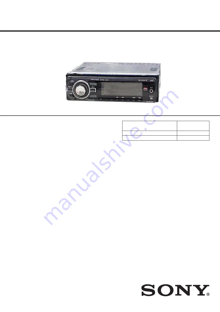
background image

SERVICE MANUAL

Published by Sony Techno Create Corporation

Sony Corporation

Audio Business Group

SPECIFICATIONS

9-889-086-01

2008D04-1

© 

2008.04

E Model

Ver. 1.0  2008.04

Model Name Using Similar Mechanism

CDX-GT527EE/
GT570/GT570S

CD Drive Mechanism Type

MG-101TC-188//Q

Optical Pick-up Name

DAX-25A

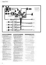
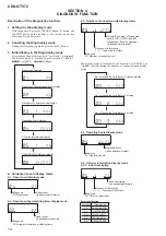
•  The tuner and CD sections have no adjustments.

CDX-GT572

FM/MW/SW COMPACT DISC PLAYER
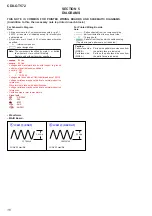
CD Player section

Signal-to-noise ratio:

 120 dB

Frequency response:

 10 – 20,000 Hz

Wow and fl utter:

 Below measurable limit

Tuner section

FM

Tuning range:

  87.5 – 108.0 MHz (at 50 kHz step)
  87.5 – 107.9 MHz (at 200 kHz step)

FM tuning interval: 


  50 kHz/200 kHz switchable

Antenna (aerial) terminal:

  External antenna (aerial) connector

Intermediate frequency:

 10.7 MHz/450 kHz

Usable sensitivity:

 9 dBf

Selectivity:

 75 dB at 400 kHz

Signal-to-noise ratio:


  67 dB (stereo), 69 dB (mono)

Harmonic distortion at 1 kHz:


  0.5 % (stereo), 0.3 % (mono)

Separation:

 35 dB at 1 kHz

Frequency response:

 30 – 15,000 Hz

MW

Tuning range:


  531 – 1,602 kHz (at 9 kHz step)
  530 – 1,710 kHz (at 10 kHz step)

MW tuning interval: 
 

9 kHz/10 kHz switchable

Antenna (aerial) terminal:

  External antenna (aerial) connector

Intermediate frequency:

 10.7 MHz/450 kHz

Sensitivity:

 30 

μ

V

SW

Tuning range:


  SW1: 2,940 – 7,735 kHz 
  SW2: 9,500 – 18,135 kHz 
  (except for 10,140


– 11,500 kHz)

Antenna (aerial) terminal:

  External antenna (aerial) connector

Intermediate frequency:

 10.7 MHz/450 kHz

Sensitivity:

 30 

μ

V

Power amplifi er section

Outputs:

 Speaker outputs (sure seal connectors)

Speaker impedance:

 4 – 8 ohms

Maximum power output:

 52 W × 4 (at 4 ohms)

General

Output:

  Audio outputs terminal (front/rear) 
  Subwoofer output terminal (mono) 
  Power antenna (aerial) relay control terminal
 Power 

amplifi er control terminal

Inputs:

  BUS control input terminal
  BUS audio input terminal
  Remote controller input terminal
  Antenna (aerial) input terminal
  AUX input jack (stereo mini jack)

Tone controls:

  Low: ±10 dB at 60 Hz (XPLOD)
  Mid: ±10 dB at 1 kHz (XPLOD)
  High: ±10 dB at 10 kHz (XPLOD)

Power requirements:

 12 V DC car battery

  (negative ground (earth))

Dimensions:

 Approx. 178 × 50 × 180 mm

 (7

 1

/

8

 × 2 × 7

 1

/

8

 in.) (w/h/d)

Mounting dimensions:

 Approx. 

  182 × 53 × 162 mm
 (7

 1

/

4

 × 2

 1

/

8

 × 6

 1

/

2

 in.) (w/h/d)

Mass:

 Approx. 1.2 kg (2 lb 11 oz)

Supplied accessories:

  Card remote commander: RM-X151
  Parts for installation and connections (1 set)

Design and specifi cations are subject to change
without notice.

Summary of Contents for CDX-GT572

Page 1: ...kHz switchable Antenna aerial terminal External antenna aerial connector Intermediate frequency 10 7 MHz 450 kHz Sensitivity 30 μV SW Tuning range SW1 2 940 7 735 kHz SW2 9 500 18 135 kHz except for 10 140 11 500 kHz Antenna aerial terminal External antenna aerial connector Intermediate frequency 10 7 MHz 450 kHz Sensitivity 30 μV Power amplifier section Outputs Speaker outputs sure seal connector...

Page 2: ...tat ic break down because of the potential difference generated by the charged electrostatic load etc on clothing and the human body During repair pay attention to electrostatic break down and also use the procedure in the printed matter which is included in the repair parts The flexible board is easily damaged and should be handled with care NOTES ON LASER DIODE EMISSION CHECK The laser beam on t...

Page 3: ...NCTION 14 TABLE OF CONTENTS 5 DIAGRAMS 5 1 Block Diagram Main Section 17 5 2 Block Diagram Display Section 18 5 3 Printed Wiring Board Main Section 19 5 4 Schematic Diagram Main Section 1 3 20 5 5 Schematic Diagram Main Section 2 3 21 5 6 Schematic Diagram Main Section 3 3 22 5 7 Printed Wiring Boards Sub Section 23 5 8 Schematic Diagram Sub Section 23 5 9 Printed Wiring Boards Key Section 24 5 10...

Page 4: ... alignment 1 Insert the AUX jack into the KEY board 2 Place the KEY board on the front panel 3 Solder the three terminals of the jack SECTION 1 SERVICE NOTE EXTENSION CABLE AND SERVICE POSITION When repairing or servicing this set connect the jig extension cable as shown below Connect the MAIN board CN350 and the SERVO board CN2 with the extension cable Part No J 2502 076 1 KEY board front panel A...

Page 5: ...stations press store stations press and hold N DSPL display SCRL scroll button page 8 To change display items press scroll the display item press and hold O RESET button page 4 P Z eject button page 5 To eject the disc Q Disc slot page 5 To insert the disc The following buttons on the card remote commander have also different buttons functions from the unit Remove the insulation film before use pa...

Page 6: ... common negative lead for the right and left speakers Do not connect the unit s speaker leads to each other Note on connection If speaker and amplifier are not connected correctly FAILURE appears in the display In this case make sure the speaker and amplifier are connected correctly Diagrama de conexión 1 A una superficie metálica del automóvil Conecte primero el cable de conexión a masa negro y d...

Page 7: ...SSY Page 8 3 2 CD MECHANISM BLOCK Page 8 SET 3 3 MAIN BOARD Page 9 3 5 CHASSIS T SUB ASSY Page 10 3 6 ROLLER ARM ASSY Page 10 3 7 CHASSIS OP ASSY Page 11 3 8 CHUCKING ARM SUB ASSY Page 11 3 9 SLED MOTOR ASSY Page 12 3 10 OPTICAL PICK UP SECTION Page 13 3 11 OPTICAL PICK UP Page 13 3 4 SERVO BOARD Page 9 ...

Page 8: ... in the numerical order given 3 1 SUB PANEL ASSY 3 2 CD MECHANISM BLOCK two claws two claws sub panel assy two screws PTT 2 6 6 flexible flat cable 17 core CN702 CN350 screw PTT 2 6 6 screw PTT 2 6 6 two screws PTT 2 6 4 bracket CD CD mechanism block ...

Page 9: ...2 5 Remove the eleven solders GRY YEL BLU ORG RED BLK RED WHT BLK RED WHT optical pick up 16 core CN1 RE MAIN board insulating sheet two screws PTT 2 6 8 screw PTT 2 6 8 three ground point screws PTT 2 6 6 two screws P 2 6 8 RB screw PTT 2 6 10 RT heat sink cord RCA two screws P 2 6 8 two screws PTT 2 6 10 screw PTT 2 6 10 CN410 3P ...

Page 10: ...CDX GT572 10 3 5 CHASSIS T SUB ASSY 3 6 ROLLER ARM ASSY chassis T sub assy claw two precision screws P 1 7 2 2 two precision screws P 1 7 2 2 washer gear RA1 roller arm assy spring RAL spring RAR ...

Page 11: ... spring damper natural coil spring damper blue chassis OP assy tension spring KF gear LE1 lever D slider R chucking arm sub assy spring Note Have this portion receive the chassis Note Have this portion receive the chassis Note Be careful not to touch the turn table ...

Page 12: ...urn table three serration screws M 2 3 three serration screws M 2 3 Note Place the stand with care not to touch the turn table Note Never remove these parts since they were adjusted Note for Assembly Note Take care to prevent the chassis from being bent when tightening the three machine screws ...

Page 13: ...ion There is space at the end of the leaf spring sub guide to avoid contact with the slide pan tapping screw M 1 4 2 5 leaf spring sub guide leaf spring OP optical pick up lead screw assy Notes for Assembly Prevent the end of the leaf spring sub guide from being in contact with the OP slide base Prevent the end of the leaf spring sub guide from being in contact with the OP slide base ...

Page 14: ...mode 4 5 CD error information display mode 4 5 1 Error description Reset count in hexadecimal format Diag code 01 Reset count Reset count in hexadecimal format Diag code 02 Number of resets by watchdog timer Shown the number of connected units for CD C MD C and XM respectivery from the rightmost in hexadecimal format Recency of information 1 3 1 represents the latest Diag code 03 Number of connect...

Page 15: ...formation Disc type CD error info history 1 latest Error description plus error details display CD error info history 3 Disc type plus operating hours display CD error info history 3 Error description plus error details display CD error info history 2 Disc type plus operating hours display CD error info history 2 Error description plus error details display CD error info history 1 latest Disc type...

Page 16: ...taken with a oscilloscope Voltage variations may be noted due to normal production tolerances Circled numbers refer to waveforms Signal path J CD PLAY F FM f MW L AUX g AUDIO For Printed Wiring Boards Note X Parts extracted from the component side Y parts extracted from the conductor side a Through hole Pattern from the side which enables seeing The other layers patterns are not indicated Caution ...

Page 17: ...EEPSIO AU_LCH AU_RCH EJECT_OK UNISO UNISI UNICLK Z MUTE CD ON CDM ON LINK_OFF SYS_RST BUS_ON B U_CHECK A ATT D_3 3V A_3 3V BU_3 3V DR_6V MECHA6V 3 3V SERVO3 3V UNISI UNISO UNISCK SYSRST LINK_OFF BUSON BUIN R CH D511 D400 D493 D491 D494 11 VDD5V 15 E2PVDD AU8V TU 5V 3 3V L 3 R 14 SDA 13 SCL 7 TUN_MUTE 6 S METER 17 E2PSDA 5 QUALITY 11 1 9 2 4 12 3 11 5 6 16 7 10 15 21 22 24 26 16 5 7 28 27 25 9 18 1...

Page 18: ...W 7 NOSE_SW LED201 DISC IN LED202 KEY MATRIX S901 915 VOLUME CONTROL DIAL SELECT BUTTON RE901 ROTARY ENCODER J370 REMOTE IN CN201 CN901 14 14 80 79 X501 32 768kHz OSCIN OSCOUT 83 82 X500 18 432MHz S201 MAIN SECTION A 3 AREASEL2 S102 FRONT PANEL DETECT LCD DRIVER LED CONTROL IC901 CL CE 77 78 76 80 COM1 I COM4 LCD901 LIQUID CRYSTAL DISPLAY PANEL 3 64 65 68 S1 I S62 DIMMER DI LED930 931 LCD BACK LIG...

Page 19: ...C306 D303 D607 C701 L300 CNJ400 TH400 C401 C405 X500 X501 S103 J1 TU1 CN350 J370 C480 C481 S102 R705 J451 CN410 C487 C461 C485 C505 IC300 S501 JW5 JW6 JW21 JW22 JW23 JW24 JW26 JW27 JW44 JW45 JW54 JW55 JW67 JW68 JW69 JW72 JW73 JW81 JW82 JW83 JW84 JW85 JW86 JW87 JW90 JW91 JW92 JW93 JW94 JW95 JW96 JW97 JW104 JW109 JW110 JW112 JW113 JW114 JW117 JW118 JW131 JW135 JW137 JW138 JW139 JW140 JW143 JW154 JW1...

Page 20: ...605 Q601 Q491 C602 JC603 JC602 C601 C901 JC504 C318 JC300 JC301 C301 C323 C704 JC302 C324 C304 C306 C305 C307 C309 C466 C465 C462 C472 IC300 C310 C320 C312 C313 C314 C315 C316 C303 FU601 CN300 R701 C902 R611 R607 R606 R602 R601 L301 L302 L303 J370 Q702 R705 Q605 CNJ400 TH400 D701 D702 L300 D602 D604 D606 D605 D603 IC601 5 4 SCHEMATIC DIAGRAM MAIN Section 1 3 See page 26 for IC Block Diagrams Page ...

Page 21: ...C443 C423 C446 C442 C422 C452 C432 JC490 C413 C414 C14 C8 C9 C3 C7 L4 C63 C64 JC400 R419 R417 R474 Q470 Q460 Q440 Q420 Q430 JC401 C480 C360 C361 C362 C364 C363 C328 C327 C331 C321 C330 C300 R355 R356 C485 C481 R482 R480 C483 C482 R361 C5 JC3 R2 R5 R4 C487 J451 J1 TU1 IC401 C494 JC305 R357 R359 R358 D2 R12 R13 L1 R6 R7 C4 5 5 SCHEMATIC DIAGRAM MAIN Section 2 3 See page 26 for IC Block Diagrams Page...

Page 22: ...17 C415 FB404 JC350 C402 R400 C412 C515 C516 JC518 JC524 C507 JC503 C523 JC501 JC508 C111 C519 C110 C109 C103 C104 C117 C116 C502 C325 R536 L500 C506 C419 C418 C410 FB407 FB406 R351 C512 C513 C510 C511 C508 C509 R577 R371 R548 R549 R517 R518 C504 S501 L101 R547 R535 IC502 R584 R551 CN350 R407 FB401 R144 R146 S103 IC602 Q501 X501 X500 IC501 S102 R525 D102 D104 D103 D110 D109 D108 D114 D115 D107 D10...

Page 23: ...2 CN201 R201 R202 LED201 LED202 1 A B C D E F G 2 3 4 5 6 7 12 12 12 12 R202 LED202 S201 CN201 CN202 R201 LED201 5 8 SCHEMATIC DIAGRAM SUB Section Page 24 Page 25 Page 22 Page 19 5 7 PRINTED WIRING BOARD SUB Section Uses unleaded solder ...

Page 24: ...C982 C983 R905 IC901 R930 R932 R992 R993 R991 R901 R914 R912 CN901 R910 R911 D905 R960 R962 FB880 FB882 FB881 Q901 R917 R952 D984 R922 R924 D907 D911 D908 D909 D903 D906 D904 D981 RE901 J901 5 9 PRINTED WIRING BOARD KEY Section Uses unleaded solder Page 23 Ref No Location Semiconductor Location D903 F 12 D904 F 11 D905 G 10 D906 F 11 D907 G 10 D908 H 11 D909 F 12 D911 H 11 Ref No Location D981 G 7...

Page 25: ...905 S904 S903 S902 S901 D911 C984 C971 C982 C983 C981 C980 IC971 LCD901 FB880 RE901 Q901 R994 J901 LED931 LED930 D982 IC901 R969 CN901 D908 D907 D909 R999 LED965 LED966 LED963 LED964 LED961 LED962 LED959 LED960 LED946 LED949 LED993 LED951 LED952 LED954 LED955 LED958 LED956 LED957 LED953 R970 R971 R972 R922 R924 R926 R928 R930 R932 R960 R962 R940 R942 R948 R950 R956 R958 R934 R936 R938 R944 R946 R9...

Page 26: ...ND3 SVR IN_RR IN_LR ACGND PGND2 VP1 STB PGND1 RST CRES REG1 GND REG5 CBU FL RL RR VP FR I 2 C BUS 1 2 3 4 5 6 7 8 9 10 14 13 12 11 BUS ON SWITCH RESET SWITCH BATTERY SWITCH BUS ON RST BATT CLK VREF GND VCC RST BUS IN CLK IN B U C DATA IN DATA OUT DATA I O 1 2 A1 100k 100k 100k 100k 100k 100k 250k 250k 250k A2 B1 3 4 B2 5 C1 6 C2 7 DP1 8 DN 9 DP2 10 DS32 11 DS12 12 DS22 13 EBIAS 14 DS21 15 DS11 16 ...

Page 27: ... communication 25 EEP_CKO O Serial clock signal output for EEPROM communication 26 AMPSTB O Stand by signal output to power amp IC 27 LCD_CE O Chip enable signal output to LCD drive IC 28 LCD_SO O Serial data signal output to LCD drive IC 29 LCD_CKO O Serial clock signal output to LCD drive IC 30 RDSON O RDS radio data system ON signal output Not used in this set Open 31 RS SEL I Rear sub switchab...

Page 28: ...n OFF 76 AD_ON O A D converter power supply control signal output 77 RESET I System reset signal input 78 NCO O Not used Open 79 XOUT O Low speed operation clock signal output 32 768 kHz 80 XIN I Low speed operation clock signal input 32 768 kHz 81 VSS1 Ground pin 82 OSCIN I High speed operation clock signal input 18 432 MHz 83 OSCOUT O High speed operation clock signal output 18 432 MHz 84 VCC3 P...

Page 29: ...NON SLIT 5 7 685 794 09 SCREW PTT 2 6X10 S Ref No Part No Description Remark Ref No Part No Description Remark Note XX and X mean standardized parts so they may have some difference from the original one Items marked are not stocked since they are seldom required for routine ser vice Some delay should be anticipated when ordering these items The mechanical parts with no reference number in the exp...

Page 30: ... 250 543 21 SCREW B P TITE M2 59 X 2187 544 1 CASE ASSY for FRONT PANEL J901 1 820 833 11 JACK SMALL TYPE VERTICAL AUX LCD901 1 802 535 11 DISPLAY PANEL LIQUID CRYSTAL RE901 1 479 902 22 ENCODER ROTARY VOLUME CONTROL DIAL SELECT BUTTON Ref No Part No Description Remark Ref No Part No Description Remark 6 2 FRONT PANEL SECTION LCD901 not supplied KEY board not supplied not supplied not supplied not...

Page 31: ...CREW M2X3 SERRATION 105 3 348 998 31 SCREW M1 4X2 5 TAPPING PAN 106 3 352 758 31 SCREW M1 7X2 5 TOOTHED LOCK 107 A 1177 201 A SERVO BOARD COMPLETE 6 7 627 000 08 SCREW PRECISION P 1 7X2 2 TYPE3 6 3 CD MECHANISM SECTION MG 101TC 188 Q not supplied 6 6 not supplied not supplied not supplied not supplied not supplied not supplied not supplied not supplied not supplied not supplied 101 102 103 105 104...

Page 32: ...6 ALBM LED959 8 719 053 08 LED SML 310DTT86 DSPL SCRL LED960 8 719 053 08 LED SML 310DTT86 6 PAUSE LED961 8 719 053 08 LED SML 310DTT86 5 LED962 8 719 053 08 LED SML 310DTT86 4 SHUF LED963 8 719 053 08 LED SML 310DTT86 3 REP LED964 8 719 053 08 LED SML 310DTT86 2 LED965 8 719 053 08 LED SML 310DTT86 1 LED966 8 719 053 08 LED SML 310DTT86 BTM LED993 8 719 053 08 LED SML 310DTT86 VOLUME ILLUMINATION...

Page 33: ...TACTILE 2 S914 1 786 653 21 SWITCH TACTILE 1 S915 1 786 653 21 SWITCH TACTILE BTM A 1312 912 A MAIN BOARD COMPLETE 7 685 134 19 SCREW P 2 6X8 TYPE2 NON SLIT 7 685 794 09 SCREW PTT 2 6X10 S CAPACITOR C2 1 126 947 11 ELECT 47uF 20 35V C3 1 162 970 11 CERAMIC CHIP 0 01uF 10 25V C4 1 107 826 11 CERAMIC CHIP 0 1uF 10 16V C5 1 126 947 11 ELECT 47uF 20 35V C7 1 162 970 11 CERAMIC CHIP 0 01uF 10 25V C8 1 ...

Page 34: ...IC CHIP 100PF 5 50V C600 1 126 941 11 ELECT 470uF 20 25V C601 1 162 970 11 CERAMIC CHIP 0 01uF 10 25V C602 1 165 319 11 CERAMIC CHIP 0 1uF 50V C701 1 112 302 11 ELECT 3300uF 20 16V C702 1 126 160 11 ELECT 1uF 20 50V C704 1 115 340 11 CERAMIC CHIP 0 22uF 10 25V C901 1 163 009 11 CERAMIC CHIP 0 001uF 10 50V C902 1 163 009 11 CERAMIC CHIP 0 001uF 10 50V CONNECTOR CN300 1 774 701 21 PIN CONNECTOR 16P ...

Page 35: ...46 Q590 8 729 027 23 TRANSISTOR DTA114EKA T146 Q600 8 729 047 76 TRANSISTOR FMC2A T148 Q601 8 729 027 23 TRANSISTOR DTA114EKA T146 Q605 8 729 027 43 TRANSISTOR DTC114EKA T146 Q702 8 729 620 07 TRANSISTOR 2SC3052EF T1 LEF RESISTOR R2 1 216 839 11 METAL CHIP 33K 5 1 10W R3 1 216 843 11 METAL CHIP 68K 5 1 10W R4 1 216 839 11 METAL CHIP 33K 5 1 10W R5 1 216 843 11 METAL CHIP 68K 5 1 10W R6 1 414 595 1...

Page 36: ...ETAL CHIP 2 2K 5 1 10W R550 1 216 845 11 METAL CHIP 100K 5 1 10W R551 1 216 864 11 SHORT CHIP 0 R553 1 216 821 11 METAL CHIP 1K 5 1 10W R554 1 216 821 11 METAL CHIP 1K 5 1 10W R555 1 216 833 11 METAL CHIP 10K 5 1 10W R556 1 216 833 11 METAL CHIP 10K 5 1 10W R557 1 216 809 11 METAL CHIP 100 5 1 10W R558 1 216 809 11 METAL CHIP 100 5 1 10W R559 1 216 845 11 METAL CHIP 100K 5 1 10W R562 1 216 845 11 ...

Page 37: ... LID BATTERY CASE for RM X151 3 217 494 32 MANUAL INSTRUCTION ENGLISH SPANISH PERSIAN 3 217 595 32 MANUAL INSTRUCTION INSTALL ENGLISH SPANISH PERSIAN X 2187 544 1 CASE ASSY for FRONT PANEL PARTS FOR INSTALLATION AND CONNECTIONS 151 X 2179 431 1 FRAME ASSY FITTING 152 1 833 974 21 CONNECTION CORD FOR AUTOMOBILE POWER 153 3 246 471 01 KEY FRAME 154 3 209 713 01 COLLAR 155 X 3381 154 1 SCREW ASSY BS4...

Page 38: ...N HISTORY Checking the version allows you to jump to the revised page Also clicking the version at the top of the revised page allows you to jump to the next revised page Ver Date Description of Revision 1 0 2008 04 New ...

Reviews: