background image

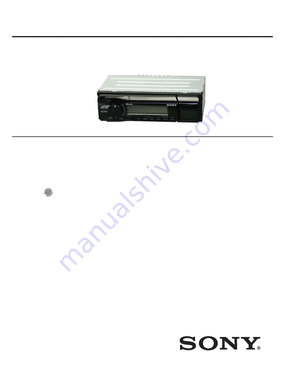
SERVICE MANUAL

Sony Corporation

Published by Sony Techno Create Corporation

DSX-M50BT

SPECIFICATIONS

9-893-910-01

2013K33-1

© 

2013.11

US Model

Canadian Model

Ver. 1.0  2013.11

•  This model is not equipped with a mechanism deck.

FOR THE CUSTOMERS IN THE USA. NOT 
APPLICABLE IN CANADA, INCLUDING IN 
THE PROVINCE OF QUEBEC.

POUR LES CLIENTS AUX ÉTATS-UNIS. NON 
APPLICABLE AU CANADA, Y COMPRIS LA 
PROVINCE DE QUÉBEC.

AUDIO POWER SPECIFICATIONS

CEA2006 Standard
Power Output: 17 Watts RMS × 4 at 
4 Ohms < 1% THD+N
SN Ratio: 80 dBA 
(reference: 1 Watt into 4 Ohms)

Tuner section

FM

Tuning range: 

87.5 – 108.0 MHz (at 50 kHz step)
87.5 – 108.0 MHz (at 100 kHz step)
87.5 – 107.9 MHz (at 200 kHz step)

USB Player section

Interface: USB (Full-speed)

Maximum current: 1 A

The maximum number of recognizable data:

Folders (albums): 128
Files (tracks) per folder: 512

Corresponding codec: 

MP3 (.mp3) and WMA (.wma)

Wireless Communication

Communication System: 

BLUETOOTH Standard version 2.1 + EDR

Output: 

BLUETOOTH Standard Power Class 2 
(Max. +4 dBm)

Maximum communication range: 

Line of sight approx. 10 m (33 ft)*

1

FM tuning step: 

50 kHz/100 kHz/200 kHz switchable

Antenna (aerial) terminal: 

External antenna (aerial) connector

Intermediate frequency: 25 kHz

Usable sensitivity: 8 dBf

Selectivity: 75 dB at 400 kHz

Signal-to-noise ratio: 80 dB (stereo)

Separation: 50 dB at 1 kHz

Frequency response: 20 – 15,000 Hz

AM

Tuning range: 

531 – 1,602 kHz (at 9 kHz step)
530 – 1,710 kHz (at 10 kHz step)

AM tuning step: 

9 kHz/10 kHz switchable

Antenna (aerial) terminal: 

External antenna (aerial) connector

Intermediate frequency: 

9,124.5 kHz or 9,115.5 kHz/4.5 kHz (at 9 kHz 
step)
9,115 kHz or 9,125 kHz/5 kHz (at 10 kHz step)

Sensitivity: 26 μV

Frequency band: 

2.4 GHz band (2.4000 – 2.4835 GHz)

Modulation method: FHSS

Compatible BLUETOOTH Profiles*

2

:

A2DP (Advanced Audio Distribution Profile) 
1.2
AVRCP (Audio Video Remote Control Profile) 
1.3
HFP (Handsfree Profile) 1.5
PBAP (Phone Book Access Profile)

*1 The actual range will vary depending on factors 

such as obstacles between devices, magnetic 
fields around a microwave oven, static 
electricity, reception sensitivity, antenna 
(aerial)’s performance, operating system, 
software application, etc.

*2 BLUETOOTH standard profiles indicate the 

purpose of BLUETOOTH communication 
between devices.

Power amplifier section

Output: Speaker outputs

Speaker impedance: 4 – 8 ohms

Maximum power output: 55 W × 4 (at 4 ohms)

General

Outputs:

Audio outputs terminal (front, rear)
Power antenna (aerial)/Power amplifier 
control terminal (REM OUT)

Inputs:

Remote controller input terminal
Antenna (aerial) input terminal
AUX input jack (stereo mini jack)
USB port

Power requirements: 12 V DC boat battery 

(negative ground (earth))

Dimensions: 

Approx. 178 mm × 50 mm × 120 mm 
(7 

1

/

8

 in × 2 in × 4 

7

/

8

 in) (w/h/d)

Mounting dimensions: 

Approx. 182 mm × 53 mm × 103 mm 
(7 

1

/

4

 in × 2 

1

/

8

 in × 4 

1

/

8

 in) (w/h/d)

Mass: Approx. 0.7 kg (1 lb 9 oz)

Package contents:

Remote commander (1): RM-X231
Parts for installation and connections (1 set)

Design and specifications are subject to 
change without notice.

FM/AM DIGITAL MEDIA PLAYER

Summary of Contents for DSX-M50BT

Page 1: ...kHz at 10 kHz step AM tuning step 9 kHz 10 kHz switchable Antenna aerial terminal External antenna aerial connector Intermediate frequency 9 124 5 kHz or 9 115 5 kHz 4 5 kHz at 9 kHz step 9 115 kHz or 9 125 kHz 5 kHz at 10 kHz step Sensitivity 26 μV Frequency band 2 4 GHz band 2 4000 2 4835 GHz Modulation method FHSS Compatible BLUETOOTH Profiles 2 A2DP Advanced Audio Distribution Profile 1 2 AVRC...

Page 2: ...at the minus side of a tantalum capacitor may be dam aged by heat The Bluetooth word mark and logos are owned by the Bluetooth SIG Inc and any use of such marks by Sony Corporation is under license Other trademarks and trade names are those of their respective owners Windows Media is either a registered trademark or trademark of Microsoft Corporation in the United States and or other countries Thi...

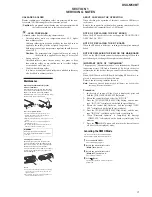
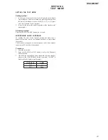
Page 3: ... checking the operation of this unit connect a USB device to this unit Refer to the support site written in the operating instruction for the details about the compatibility of a USB device NOTE OF REPLACING THE KEY BOARD When the KEY board is defective exchange the FRONT PANEL ASSY Ref No FP1 NOTE OF REPLACING THE BT BOARD When the BT board is defective exchange the complete mounted board NOTE OF...

Page 4: ...K M button The digit returns by pressing the MODE or SEEK m button 3 The setting is completed by pressing the PUSH ENTER SE LECT button and the initialization operation is done Method of operation by remote commander 1 Press the V or v button and select the alphanumeric char acter of 0 to F 2 The digit advances by pressing the b button The digit returns by pressing the B button 3 The setting is co...

Page 5: ...n lights 2 Playback Bluetooth audio Confirm the sound is emitted from this unit when this unit is switched to Bluetooth Audio source 3 Confirm whether Bluetooth audio can be controlled by oper ating this unit the SEEK M SEEK m and PAUSE 3 buttons operation Note Varies depending on the connected Bluetooth audio device 8 What to Do after Checking After checking select BT INIT from the menu list of t...

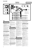
Page 6: ...ción aunque apague el interruptor de encendido Notas sobre la conexión de los altavoces ˎ Antes de conectar los altavoces desconecte la alimentación de la unidad ˎ Utilice altavoces con una impedancia de 4 a 8 Ω con la capacidad de potencia adecuada para evitar que se dañen ˎ No conecte los terminales de altavoz al chasis del barco ni conecte los terminales del altavoz derecho con los del izquierd...

Page 7: ...supplied Operating Instructions ˎ If replacing the boat battery or changing the connections the tuning step setting will be erased Français Précautions ˎ Choisissez soigneusement l emplacement d installation pour que l appareil ne gêne pas la conduite du bateau ou de la voiture ˎ Évitez d installer l appareil dans un endroit exposé à la poussière à la saleté à des vibrations excessives ou à des te...

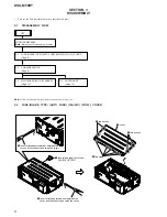
Page 8: ...SSY Note Illustration of disassembly is omitted 3 5 ANTENNA BT Page 10 2 Insert a flathead screwdriver between the cover and the chassis and raise the cover 2 Insert a flathead screwdriver between the cover and the chassis and raise the cover 5 cover 4 five claws 3 two bosses 3 two bosses 1 fuse blade type auto fuse 10A 32V FU101 Note Follow the disassembly procedure in the numerical order given 3...

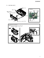
Page 9: ...de connector CN1004 4 two claws 5 sub panel block Note 1 Where USB cover is closed remove the sub panel block antenna BT USB cover OK NG close open Note 2 Where USB cover is closed attach the sub panel block Antenna BT may be damaged if it pushes in strongly where USB cover is opened QQHU YLHZ contact front side microphone wire filament tape BT board MAIN board ...

Page 10: ...NA BT 1 lead wire with connector CN1006 2 screw T 3 antenna BT LUH VHWWLQJ connector connector lead wire with connector lead wire with connector BT board lead wire with connector connector CN1006 antenna BT front side MAIN board filament tape OK NG Note 1 When the complete MAIN board is replaced it is necessary to confirm operation Refer to BLUETOOTH FUNCTION CHECKING METHOD USING A CELLULAR PHONE...

Page 11: ...od Press the SOURCE OFF button for 1 second MICROPHONE AUDIO LOOPBACK To confirm the state of the internal microphone used when a handsfree function is used the microphone audio is output from the speaker The breakdown judgment of the microphone can be done without connecting H F with the cellular phone Procedure 1 Enter the test mode 2 Press the SOURCE OFF button to select the Bluetooth Phone fun...

Page 12: ...DSX M50BT 12 MEMO ...

Page 13: ...IN MIC_OUT LCH_P LCH_N SDA SCL RSTN R CH ANT601 MIC601 RCH_P RCH_N UART_TX UART_RX UART_RTS UART_CTS MUTE RESET MODULE_PON MIX AMP IC602 SIFDO SDI 53 22 SIFDI SDO 52 21 SIFCK SCK 55 19 SIFCE CE 22 MUTE 16 AC_GND 4 STBY 56 17 BUSYB BUSY 86 16 CMDERR CMD_ERR 62 23 USBINS1 USB_IN 47 25 SMON1 WDT_MON 51 18 RESETB SYSRST LINE AMP IC302 EEPROM IC202 MUTING Q305 MUTING Q303 X201 12MHz 75 2 SCL 6 74 X12IN...

Page 14: ...0 99 LCD_SO 100 LCD_CLK 98 LCD_CE 89 FLT_USB 81 BT_MIC_ON A50 74 AUDIO_EN 73 SYS_EN 10 RESET 90 KEYACK0 KEYACK1 KEY BOARD LCD_DATA LCD_CLK LCD_CE SIRCS KEY_1 KEY_0 RE_1 RE_0 PANEL_SW X102 7 92MHz 11 OSCOUT 13 OSCIN 3 3V REGULATOR IC102 3 3V REGULATOR IC601 RESET SIGNAL GENERATOR IC105 B SWITCH Q102 SYS 3 3V BT 3 3V 5V REGULATOR IC603 TU 5V 59 ILL_ON 9V REGULATOR IC402 ILL 9V AUDIO 8 5V 15 REG 3 3V...

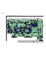
Page 15: ...oted due to normal production tolerances Circled numbers refer to waveforms Signal path F AUDIO f TUNER d USB E AUX a Bluetooth N MIC Caution Pattern face side Conductor Side Parts face side Component Side Parts on the pattern face side seen from the pattern face are indicated Parts on the parts face side seen from the parts face are indicated Indication of transistor C B These are omitted E Q Not...

Page 16: ...133 R328 R329 R138 R139 R330 R331 C101 R332 C102 R333 R334 R140 C105 R335 R336 C106 R143 C301 R149 C302 C303 C304 C110 C305 C306 C308 C309 R152 R153 R154 C119 R155 C502 R156 R157 C310 C504 R158 C505 R159 C313 C314 C508 CL201 C509 CL202 C122 C317 CL203 R160 C319 CL011 R161 R162 CL012 CL013 C510 CL014 C511 CL015 R165 CL016 C513 R167 CL017 C320 C514 CL018 R168 C321 C515 R169 CL019 C322 C516 C323 C517...

Page 17: ...2 TU252 TUX DSP03 TUNER UNIT CN201 J304 C341 MAIN BOARD CONDUCTOR SIDE 1 889 211 11 11 E E K A E E A K L R REAR L R FRONT AUDIO OUT AUX KEY BOARD BT BOARD MIC601 ANT601 A B C D E F G H 1 2 3 4 5 6 7 8 9 10 11 12 1 9 17 18 19 16 8 WR1 1 9 WHT BLK WHT GRN BLK GRN VIO BLK VIO GRY BLK GRY RED YEL BLK FRONT LCH FRONT LCH REAR LCH REAR LCH REAR RCH REAR RCH FRONT RCH FRONT RCH ACC BATT GND 2 10 3 11 4 1...

Page 18: ...6US H IC201 1 LFOUT 2 LROUT 3 LVRIN 4 DACOUT_L 5 DACOUT_R 6 RVRIN 7 RROUT 8 RFOUT 9 L1_IN 10 R1_IN 11 L2_IN 12 R2_IN 13 L3_IN_P 14 L3_IN_N 15 R3_IN_P 16 R3_IN_N 17 ATEST01 OPN 18 ATEST02 OPN 19 VREFOUT 20 VREF_ADC 21 AVSS2 22 AVDD2 23 NC 24 NC 25 NC 26 NC 27 NC 28 NC 29 NC 30 NC 31 DVDD 32 DVSS 33 NC 34 NC 35 NC 36 NC 37 NC 38 NC 39 NC 40 NC 41 DVDD 42 DVSS 43 REG1_EXTR OPN 44 DVDD15 45 iTXD 46 iR...

Page 19: ...E 45 HIT2_SDA 46 HIT2_SCL 47 HIT2_RESET 48 EN_USB 49 NC 50 FLT_USB 51 EN_SYS 52 IPOD 53 NC 54 TELATT 55 ACC_IN 56 ATT 57 AMP_MUTE 58 AMPSTB 59 ILL_ON 60 VCC2 61 NC 62 VSS 63 NC 64 NC 65 BT_MUTE A50 66 BU_IN 67 NC 68 NC 69 NC 70 NC 71 NC 72 AMP_REM 73 SYS_EN 74 AUDIO_EN 75 BT_TX A50 76 BT_RX A50 77 NC 78 NC 79 RE IN0 80 RE IN1 81 BT_MIC_ON A50 82 BT_RTS A50 83 BT_CTS A50 84 BT_RESET A50 85 BT_POWER...

Page 20: ... D107 Z2J18000L D114 47p C333 C638 47p CN102 16P 1 FL 2 RL 3 RR 4 FR 5 AMP REM 6 ANT REM 7 ACC 8 GND 9 FL 10 RL 11 RR 12 FR 16 B 13 TEL ATT 14 ILL 15 TEST 17 B 18 B 19 B LTC044EUBFS8TL Q101 LTC014YUBFS8TL Q110 LTC014EUBFS8TL Q103 LTA014EUBFS8TL Q109 LTC014EUBFS8TL Q304 C401 16V 3300 PURE5001H 4WX IC304 1 TAB 2 PW_GND2 FL 3 FL 4 STBY 5 FL 6 VCC2 7 RL 8 PW_GND1 RL 9 RL 10 RIPPLE 11 IN_RL 12 IN_FL 13...

Page 21: ...OUT2 3 ST BY 4 OUT2 5 VCC2 6 OUT1 7 PW GND1 8 OUT1 9 SVR 10 IN1 11 AC GND 16 OUT3 17 PW GND3 18 OUT3 19 VCC1 20 OUT4 21 MUTE 22 OUT4 23 PW GND4 24 HSD 25 IN3 15 IN4 14 S GND 13 IN2 12 HIGH SIDE DRIVER IC401 LV56831P E NC 1 NC 4 NC 7 VCC 8 VCC1 9 AUDIO_EN 2 REG_EN 10 IKREG 11 AMP_EN 12 AMP 13 GND 14 AUDIO 3 VDD 5 IKVDD 6 REG 15 START UP VREF OVER VOLTAGE PROTECTION THERMAL SHUTDOWN OUTPUT CONTROL ...

Page 22: ...VIN 3 EN_SYS 4 USBOUT 5 ISET_USB 10 RT 15 VREF 16 FB_USB 6 USBIN 2V UVLS 7 SYNC 8 GNDA 14 VIC_USB 11 SS_SYS 13 EN_USB 12 HDR OSCILLATOR REFERENCE GENERATOR OVER CURRENT PROTECTION VS SEL Q S R ADJUSTMENT GENERATOR CHARGE PUMP OVER CURRENT LIMIT USB FAULT PROTECITON VOUT_SYS USBIN FAULT PROTECTION IC603 NJM2884U2 05 TE2 5 VIN 4 VOUT 2 GND 3 N C 1 CONTROL BANDGAP REFERENCE THERMAL PROTECTION ...

Page 23: ...o DSP 26 BEEP O Beep sound output to the power amplifier 27 28 NC Not used 29 FW_TXD O Serial data output terminal for flash writing 30 FW_RXD I Serial data input terminal for flash writing 31 FW_CLK I Serial data transfer clock signal input terminal for flash writing 32 FW_BUSY O Busy signal output terminal for flash writing 33 to 38 NC Not used 39 EPM O EPM signal output terminal Fixed at L in t...

Page 24: ...o send signal input from the Bluetooth section 84 BT_RESET A50 O Reset signal output to the Bluetooth section L reset 85 BT_POWER A50 O Power supply on off control signal output to the Bluetooth section H power on 86 NC Not used 87 SYS_ON O System power on off control signal output terminal L power on 88 RCIN1 I Rotary commander shift key input terminal 89 KEYACK0 I Key acknowledge signal wake up ...

Page 25: ...3V for digital system 42 DVSS Ground terminal for digital system 43 REG1_EXTR OPN Internal regulator reserve terminal Not used 44 DVDD15 External capacitor connection terminal for internal regulator 45 iTXD O Serial data output terminal Not used 46 iRXD I Serial data input terminal Not used 47 SMONI O Watch dog timer status monitor output to the system controller 48 NC Not used 49 DVDD Power suppl...

Page 26: ...terminal for digital system 90 DVDD15 External capacitor connection terminal for internal regulator 91 JTRSTB IPD I Reset signal input terminal for JTAG Normally fixed at L 92 JTCK IPD I Clock signal input terminal for JTAG Normally fixed at L 93 JTDI IPD I Data input terminal for JTAG Normally fixed at L 94 JTMS IPU I Mode selection signal input terminal for JTAG Normally fixed at H 95 JTDO O O D...

Page 27: ...ef No Part No Description Remark Ref No Part No Description Remark Note XX and X mean standardized parts so they may have some difference from the original one Items marked are not stocked since they are seldom required for routine ser vice Some delay should be anticipated when ordering these items The mechanical parts with no reference number in the exploded views are not sup plied Color Indicati...

Page 28: ...MIC CHIP 10uF 20 6 3V C235 1 116 720 11 CERAMIC CHIP 10uF 20 6 3V C236 1 125 777 11 CERAMIC CHIP 0 1uF 10 10V C237 1 112 298 91 CERAMIC CHIP 1uF 10 16V C238 1 164 852 11 CERAMIC CHIP 12PF 5 50V C239 1 112 298 91 CERAMIC CHIP 1uF 10 16V C240 1 164 940 11 CERAMIC CHIP 0 0033uF 10 16V C241 1 164 882 11 CERAMIC CHIP 220PF 5 16V C244 1 125 777 11 CERAMIC CHIP 0 1uF 10 10V C245 1 165 492 21 ELECT CHIP 1...

Page 29: ...10 25V C502 1 100 591 91 CERAMIC CHIP 1uF 10 25V C504 1 114 334 11 CERAMIC CHIP 10uF 10 25V C505 1 114 334 11 CERAMIC CHIP 10uF 10 25V C508 1 100 672 11 CERAMIC CHIP 10uF 20 16V C509 1 164 943 81 CERAMIC CHIP 0 01uF 10 16V C510 1 164 936 11 CERAMIC CHIP 680PF 10 50V C511 1 100 055 21 CERAMIC CHIP 22uF 20 16V C513 1 100 567 81 CERAMIC CHIP 0 01uF 10 25V C514 1 114 330 11 CERAMIC CHIP 2 2uF 10 16V C...

Page 30: ...METAL CHIP 100K 5 1 16W R152 1 218 941 81 METAL CHIP 100 5 1 16W R153 1 218 941 81 METAL CHIP 100 5 1 16W R154 1 218 941 81 METAL CHIP 100 5 1 16W R155 1 218 941 81 METAL CHIP 100 5 1 16W R156 1 218 941 81 METAL CHIP 100 5 1 16W R157 1 218 949 11 METAL CHIP 470 5 1 16W R158 1 218 941 81 METAL CHIP 100 5 1 16W R159 1 218 941 81 METAL CHIP 100 5 1 16W R160 1 218 941 81 METAL CHIP 100 5 1 16W R161 1 ...

Page 31: ...3 11 METAL CHIP 220 5 1 10W R326 1 218 945 11 METAL CHIP 220 5 1 16W R327 1 218 965 11 METAL CHIP 10K 5 1 16W R328 1 218 965 11 METAL CHIP 10K 5 1 16W R329 1 218 945 11 METAL CHIP 220 5 1 16W R330 1 218 945 11 METAL CHIP 220 5 1 16W R331 1 218 965 11 METAL CHIP 10K 5 1 16W R332 1 218 965 11 METAL CHIP 10K 5 1 16W R333 1 218 945 11 METAL CHIP 220 5 1 16W R334 1 218 965 11 METAL CHIP 10K 5 1 16W R33...

Page 32: ... 489 810 42 REMOTE COMMANDER RM X231 4 484 593 21 MANUAL INSTRUCTION ENGLISH FRENCH SPANISH 4 484 594 11 MANUAL INSTRUCTION INSTALL ENGLISH FRENCH SPANISH PARTS FOR INSTALLATION AND CONNECTIONS 501 X 2583 962 1 FRAME ASSY FITTING 502 4 276 003 01 KEY FRAME 1 piece 503 1 846 997 11 CONNECTION CABLE AUTOMOBILE POWER 504 4 168 810 02 COLLAR 505 3 934 325 21 SCREW K 5X8 TAPPING 1 piece FITTING FRAME A...

Page 33: ...MEMO DSX M50BT 33 ...
Page 34: ...N HISTORY Checking the version allows you to jump to the revised page Also clicking the version at the top of the revised page allows you to jump to the next revised page Ver Date Description of Revision 1 0 2013 11 New ...

Reviews: