background image

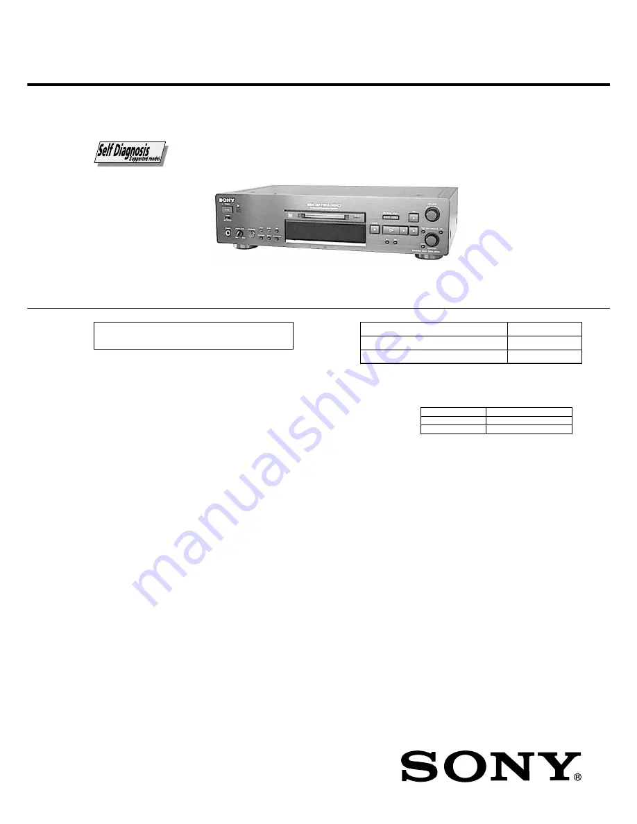
MDS-JB940

US Model

Canadian Model

AEP Model

UK Model

SERVICE MANUAL

MINIDISC DECK

Model Name Using Similar Mechanism

NEW

MD Mechanism Type

MDM-7A

Optical Pick-up Name

KMS-260B/J1N

U.S and foreign patents licensed from Dolby
Laboratories Licensing Corporation.

SPECIFICATIONS

Inputs

Outputs

System

MiniDisc digital audio system

Disc

MiniDisc

Laser

Semiconductor laser (

λ

 = 780 nm) 

Emission duration:  continuous

Laser output

MAX 44.6 

µ

W

1)

1) This output is the value 

measured at a distance of 
200 mm from the objective lens 
surface on the Optical Pick-up 
Block with 7 mm aperture.

Laser diode

Material: GaAlAs

Revolutions (CLV)

400 rpm to 900 rpm 

Error correction

ACIRC (Advanced Cross Interleave 
Reed Solomon Code)

Sampling frequency

44.1 kHz

Coding

ATRAC (Adaptive TRansform 
Acoustic Coding)/ATRAC 3

Modulation system

EFM (Eight-to-Fourteen 
Modulation)

Number of channels

2 stereo channels

Frequency response

5 to 20,000 Hz 

±

0.3 dB

Signal-to-noise ratio

Over 100 dB during play

Wow and flutter

Below measurable limit

ANALOG IN

Jack type:  phono
Impedance:  47 kilohms
Rated input:  500 mVrms 
Minimum input:  125 mVrms

DIGITAL OPTICAL IN1

Connector type:  square optical
Impedance:  660 nm (optical wave 
length)

DIGITAL OPTICAL IN2

Connector type:  square optical
Impedance:  660 nm (optical wave 
length)

DIGITAL COAXIAL IN

Jack type:  phono
Impedance:  75 ohms
Rated input:  0.5 Vp-p, 

±

20 %

PHONES

Jack type:  stereo phone
Rated output:  28 mW
Load impedance:  32 ohms

ANALOG OUT

Jack type:  phono
Rated output:  2 Vrms (at 50 
kilohms)
Load impedance:  over 10 kilohms

DIGITAL OPTICAL OUT

Connector type:  square optical
Rated output:  –18 dBm
Load impedance:  660 nm (optical 
wave length)

DIGITAL COAXIAL OUT

Jack type:  phono
Rated output:  0.5 Vp-p (at 75 ohms)
Load impedance:  75 ohms

General

Power requirements

Supplied accessories

US and foreign patents licensed from Dolby Laboratories.

Design and specifications are subject to change without 
notice.

Where purchased

Power requirements

U.S.A. and Canada

120 V AC, 60 Hz

Europe

230 V AC, 50/60 Hz

Power consumption

18 W

Dimensions (approx.)

430 

×

 111 

×

 286 mm (17 

×

 4

3

/

8


×


11

3

/

8

 in.) (w/h/d) incl. projecting 

parts and controls

Mass (approx.)

5.3 kg (11 lbs 11 oz)

This MD deck comes with the following items:


Audio connecting cords (2)


Optical cable (1)


Remote commander (remote) (1)


R6 (size-AA) batteries (2)

Summary of Contents for MDS-JB940

Page 1: ...Impedance 47 kilohms Rated input 500 mVrms Minimum input 125 mVrms DIGITAL OPTICAL IN1 Connector type square optical Impedance 660 nm optical wave length DIGITAL OPTICAL IN2 Connector type square optical Impedance 660 nm optical wave length DIGITAL COAXIAL IN Jack type phono Impedance 75 ohms Rated input 0 5 Vp p 20 PHONES Jack type stereo phone Rated output 28 mW Load impedance 32 ohms ANALOG OUT...

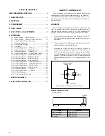
Page 2: ...itable See Fig A SAFETY CHECK OUT To Exposed Metal Parts on Set 0 15 µF 1 5 kΩ AC Voltmeter 0 75V Earth Ground Fig A Using an AC voltmeter to check AC leakage TABLE OF CONTENTS MODEL IDENTIFICATION BACK PANEL Model AEP UK models Canadian model US model Part No 4 228 507 0s 4 228 507 1s 4 228 507 2s Part No SELF DIAGNOSIS FUNCTION 4 1 SERVICE NOTE 6 2 GENERAL 11 3 DISASSEMBLY 14 4 TEST MODE 17 5 EL...

Page 3: ... ved feilaktig skifte av batteri Benytt samme batteritype eller en tilsvarende type anbefalt av apparatfabrikanten Brukte batterier kasseres i henhold til fabrikantens instruksjoner VARNING Explosionsfara vid felaktigt batteribyte Använd samma batterityp eller en likvärdig typ som rekommenderas av apparattillverkaren Kassera använt batteri enligt gällande föreskrifter VAROITUS Paristo voi räjähtää...

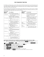
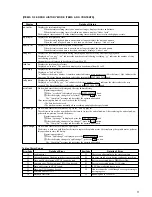
Page 4: ...o return to step 4 8 Press the MENU NO button to display Err Display and release the error history mode 9 To release the test mode press the REPEAT button The unit sets into the STANDBY state and the test mode ends Three or five digit code Message Cause Remedy C11 Protected The inserted MD is record protected Take out the MD and close the record protect slot page 15 C12 Cannot Copy You tried to re...

Page 5: ...ess the l AMS L knob 2 After the display changes to er refresh press the YES button The Complete message indicates that the operation has ended After executing this mode be sure to check the following The data has been erased The mechanism runs normally when recording and playback are performed Mode which erases the total time of op rec tm and op play tm These histories are used as a guideline for...

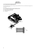
Page 6: ...nd I 3V For measuring IOP Check the deterioration of the optical pick up laser IOP For measuring IOP Check the deterioration of the optical pick up laser TEO TRK error signal Traverse adjustment VC Reference level for checking the signal RF RF signal Check jitter FE FOCUS error SECTION 1 SERVICE NOTE CN105 RF VC TE IOP I 3V GND Mechanism deck RF VC for MDM 7 IOP TE I 3V GND VC RF TE IOP I 3V GND 1...

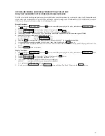
Page 7: ...nged will blink 5 Input the IOP value written on the optical pick up label To select the number Turn the l AMS L knob To select the digit Press the l AMS L knob 6 When the YES button is pressed the display becomes Measu is an arbitrary number 7 As the adjustment results are recorded for the 6 value Leave it as it is and press the YES button 8 Complete will be displayed momentarily The value will b...

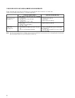
Page 8: ...isconnection of the circuits around D101 BD board Check the signals around IC101 IC151 CN102 CN103 BD board Note The criteria for determination above is intended merely to determine if satisfactory or not and does not serve as the specified value for adjustments When performing adjustments use the specified values for adjustments Criteria for Determination Unsatisfactory if specified value is not ...

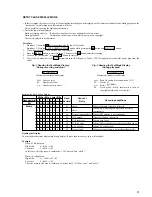
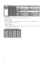
Page 9: ...er of retry errors Fig 2 Reading the Test Mode Display During playback Fluorescent indicator tube display Parts No name of area named on TOC Cluster Sector Track mode Track information such as copyright information of each part Higher Bits Lower Bits 8 4 2 1 8 4 2 1 b7 b6 b5 b4 b3 b2 b1 b0 0 0 0 0 0 0 0 1 0 0 0 0 0 0 1 0 0 0 0 0 0 1 0 0 0 0 0 0 1 0 0 0 0 0 0 1 0 0 0 0 0 0 1 0 0 0 0 0 0 1 0 0 0 0 0...

Page 10: ...he retry cause is combined of emphasis ON stereo original copyright exists and write prohibited Hexadecimal t Binary Conversion Table Hexadecimal Binary Hexadecimal Binary 0 0000 8 1000 1 0001 9 1001 2 0010 A 1010 3 0011 B 1011 4 0100 C 1100 5 0101 D 1101 6 0110 E 1110 7 0111 F 1111 Higher Bits Lower Bits 8 4 2 1 8 4 2 1 b7 b6 b5 b4 b3 b2 b1 b0 0 0 0 0 0 0 0 1 0 0 0 0 0 0 1 0 0 0 0 0 0 1 0 0 0 0 0...

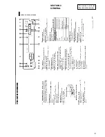
Page 11: ...11 SECTION 2 GENERAL This section is extracted from instruction manual ...

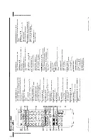
Page 12: ...12 ...

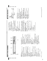
Page 13: ...13 ...

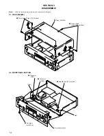
Page 14: ... the numerical order given 3 1 CASE 4095269 1 Four screws Screw TP flat head 3 Case 4095269 2 Three screws Screw TP flat head 3 2 FRONT PANEL SECTION Claw 4 Six screws BVTP3 8 Claw 5 Front panel section 1 Connector CN800 2 Connector CN801 3 Wire flat type 19 core CN2 ...

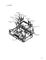
Page 15: ... core CN12 1 Wire flat type 19 core CN2 8 Wire flat type 23 core CN11 qs AU board 6 Connector CN700 q Four screws BVTP 3 8 9 Screw BVTP 3 8 5 Connector CN401 4 Connector CN403 3 Connector CN404 2 Connector CN200 qa Seven screws BVTP 3 8 ...

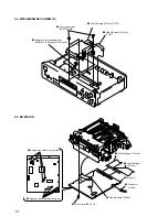
Page 16: ...7A to direction of the arrow 2 Wire flat type 23 core CN11 1 Wire flat type 27 core CN12 3 5 BD BOARD 5 Remove the solder four portions 4 Remove the solder five portions 6 Two screws BTP 2 6 8 Flexible board CN104 3 Connector CN104 7 BD board 1 Wire flat type 23 core 2 Wire flat type 27 core ...

Page 17: ... The following are two methods of entering the test mode Procedure 1 While pressing the lAMS L knob and x button connect the power plug to an outlet and release the lAMS L knob and x button When the test mode is set Check will be displayed Turn the l AMS L knob switches between the following three groups y Check y Service y Develop y Procedure 2 While pressing the l AMS L knob connect the power pl...

Page 18: ...DJUS EF CD ADJUS FBIAS ADJUS AG Set MO AG Set CD TEMP CHECK LDPWR CHECK EF MO CHECK EF CD CHECK FBIAS CHECK ScurveCHECK VERIFYMODE DETRK CHECK 0920 CHECK Iop Read Iop Compare ADJ CLEAR INFORMATION CPLAY 1 MODE CREC 1 MODE No C01 C02 C03 C04 C05 C06 C07 C08 C09 C10 C11 C12 C13 C14 C15 C16 C17 C18 C19 C25 C26 C27 C28 C31 C34 C35 Contents Auto self diagnosis Error history display delete Temperature c...

Page 19: ... 1 Entering the continuous recording mode 1 Set a recordable disc in the unit 2 Turn the l AMS L knob and display CREC 1 MODE C34 3 Press the YES button to change the display to CREC 1 MID 4 When access completes the display changes to CREC 1 and REC lights up Note The numbers displayed shows you the recording position addresses 2 Changing the parts to be recorded 1 When the YES button is pressed ...

Page 20: ...be read appears Displays other than the above are not used for service Contents Sets continuous playback when pressed in the STOP state When pressed during continuous playback the tracking servo turns ON OFF Stops continuous playback and continuous recording The sled moves to the outer circumference only when this is pressed The sled moves to the inner circumference only when this is pressed Switc...

Page 21: ...d in step 2 When DISC IN appears load the TDYS 1 check disc MD 5 After the disc loaded in step 4 is loaded the check automatically restarts from 07 CHECK 6 After the check of item 12 is complete OK or NG appears When all items are OK CHECK ALL OK appears If even one of the items failed NG xxxx appears When CHECK ALL OK appears there is no problem in the optical pick up Check the operations of the ...

Page 22: ...JUSTMENT If a defect such as dropout caused by the OP is found check the following Check Procedure Before Replacement NG NG NG OK OK OK Start Laser power check Iop Compare AUTO CHECK Replace the OP or replace the MDM Mechanism check of sled etc Other cause is likely ...

Page 23: ...D101 Replace either OP IC190 or IC195 Replace either OP IC102 IC190 or IC195 Replace either OP IC101 IC151 or IC195 Replace the OP op change in Err Display mode Iop Write Replace the spindle motor spdl change in Err Display mode AUTO CHECK End adjustment TEMP ADJUST LDPWR ADJUST Iop NV Save EF MO CD ADJUST FBIAS ADJUST AG SET MO CD YES YES YES YES YES YES YES YES ...

Page 24: ...er Thermometer Jig for checking BD board waveform Part No J 2501 196 A for MDM 7A 5 When observing several signals on the oscilloscope etc make sure that VC and ground do not connect inside the oscilloscope VC and ground will become short circuited 6 Using the above jig enables the waveform to be checked without the need to solder Refer to Servicing Notes on page 6 7 As the disc used will affect t...

Page 25: ...nt IOP value when 7 mW laser power is output and the reference IOP value normally the value when shipped from the factory written in the non volatile memory are compared and the degree of increase or decrease is shown as a percentage Note Do the following operation when the temperature of the optical pick up is almost the same as room temperature Operation Procedure 1 Turn the l AMS L knob to disp...

Page 26: ... offset value 11 Press the YES button to display EF MO CHECK The disc stops rotating automatically 12 Press the EJECT A button and take out the disc 13 Load the check disc MD TDYS 1 14 Turn the lAMS L knob and display EF CD CHECK C15 15 Press the YES button to display EFB CD Servo is imposed automatically 16 Observe the waveform of the oscilloscope and check that the specified value is satisfied D...

Page 27: ... initial setting will be executed after which ADJ CLEAR will be displayed 5 8 RECORDING AND DISPLAYING THE IOP INFORMATION The IOP data can be recorded in the non volatile memory The IOP value on the optical pick up label and the IOP value after the adjustment will be recorded Recording these data eliminates the need to read the label on the optical pick up Recording Procedure 1 Turn the l AMS L k...

Page 28: ...n to display LDPWR CHECK and stop the laser emission The MENU NO button is effective at all times to stop the laser emission 11 Turn the l AMS L knob to display Iop Write C05 Optical pick up objective lens Laser power meter BD board Digital voltmeter CN105 pin 1 I 3V CN105 pin 2 IOP KMS 260B 27X40 B0825 lOP 82 5 mA in this case lOP mA Digital voltmeter reading mV 1 Ω Optical pick up label 12 Press...

Page 29: ...ess the YES button and save the adjustment results in the non volatile memory EFB SAV will be displayed for a moment 10 EFB MO P will be displayed The optical pick up moves to the pit area automatically and servo is imposed 11 Turn the l AMS L knob until the waveform of the oscilloscope moves closer to the specified value In this adjustment waveform varies at intervals of approx 2 Adjust the wavef...

Page 30: ...R is 00 6 Press the MENU NO button to stop playback then press the EJECT A button and take out the test disc 5 15 FOCUS BIAS CHECK Change the focus bias and check the focus tolerance amount Checking Procedure 1 Load the continuously recorded disc MDW 74 GA 1 Refer to 5 Creating Continuously Recorded Disc 2 Turn the lAMS L knob to display CPLAY 1 MODE C34 3 Press the YES button twice to display CPL...

Page 31: ...XCAS 46 XRAS 34 31 36 40 45 AO0 AO9 9 12 14 18 5 1 2 24 25 WE 3 OE 22 CAS 23 DO0 DO3 49 48 50 51 DIG RST 47 WRPWR 35 MOD 14 IOP 133 LDON 29 RXO 45 TXO 44 22 DADTI SYSTEM CONTROL IC1 1 2 CLKO 46 24 XBCKI LRCK 34 23 LRCKI MNT1 58 2 MNT1 MNT2 56 3 MNT2 SRDT 40 8 SRDT SENS 48 9 SENS SWDT 38 5 SWDT SCLK 42 6 SCLK XLATCH 50 7 XLAT SQSY 27 11 SQSY DQSY 25 12 DQSY XINT 32 14 XINT 126 OPT1 OPT1 127 COAX OP...

Page 32: ...CLK 36 IIC DATA 37 KEYBOARD DATA 116 KEYBOARD CLK 28 KEYBOARD CLK CTRL 114 A1 IN 3 A1 OUT 31 1 DATA FL 2 CLK FL 128 CS FL FUCTION KEY KEY3 137 S731 733 TIMER TIMER 136 S751 X2 32 768kHz 18 CLOCK OUT 17 CLOCK IN A0 A18 31 29 33 35 38 40 42 44 32 30 34 36 39 41 43 45 92 85 77 75 100 94 122 119 131 102 73 3 37 79 80 1 2 8 1 48 17 25 18 16 DQ0 DQ15 A1 A19 D0 D15 FLASH ROM IC2 WE 11 WP 14 CE 26 OE 28 6...

Page 33: ...orms are taken with a oscilloscope Voltage variations may be noted due to normal produc tion tolerances Circled numbers refer to waveforms Signal path E PB ANALOG OUT a PB DIGITAL OUT q REC ANALOG IN r REC DIGITAL IN Abbreviation CND Canadian model Caution Pattern face side Parts on the pattern face side seen from Side B the pattern face are indicated Parts face side Parts on the parts face side s...

Page 34: ... qh OSCI 5 IC151 wj LRCK 6 IC151 wk XBCK 7 IC151 o FS4 8 IC171 3 1 3 Vp p 0 2 Vp p 1 6 Vp p 3 1 Vp p 3 2 Vp p 3 8 Vp p 3 2 Vp p 45 158 MHz 44 1 kHz 2 8224 MHz 176 4 kHz 1 0 Vp p 45 158 MHz MAIN Board 1 IC1 w XOUT 2 IC1 qk CLOCK 3 IC201 qs XOUT 3 Vp p 10 MHz 1 6 Vp p 32 768 MHz 5 2 Vp p 45 158 MHz ...

Page 35: ...e 43 Page 43 Ref No Location Semiconductor Location Ref No Location D101 A 1 A D181 D 3 B D183 D 3 B IC101 A 3 B IC102 B 3 B IC141 C 1 B IC151 C 2 B IC153 C 3 B IC171 D 2 B IC181 D 3 B IC190 D 1 B IC195 D 2 B Q101 B 1 A Q121 B 3 B Q122 B 3 B Q131 C 1 A Q132 B 1 A Q133 B 1 A Q134 C 1 A Q181 D 3 B Q182 D 3 B ...

Page 36: ...MDS JB940 36 36 6 7 SCHEMATIC DIAGRAM BD Board 1 2 See page 34 for Waveforms See page 48 for IC Block Diagrams See page 53 for IC Pin Function KMS 260B J1N 1 2 3 PIN FUNCTION ...

Page 37: ...MDS JB940 37 37 6 8 SCHEMATIC DIAGRAM BD Board 2 2 See page 34 for Waveforms See page 49 for IC Block Diagrams See page 54 for IC Pin Function Page 39 Page 40 PIN FUNCTION ...

Page 38: ...oard KEY Board 6 10 SCHEMATIC DIAGRAM HP Board KEY Board See page 52 for IC Block Diagram Page 42 Page 42 Page 39 Page 41 There are few cases that the part printed on this diagram isn t mounted in this model See page 33 for Circuit Board Location ...

Page 39: ...MDS JB940 39 39 6 11 SCHEMATIC DIAGRAM MAIN Board 1 3 See page 34 for Waveforms See page 57 for IC Pin Function Page 38 Page 45 Page 37 PIN FUNCTION ...

Page 40: ...MDS JB940 40 40 6 12 SCHEMATIC DIAGRAM MAIN Board 2 3 See page 50 for IC Block Diagrams Page 37 Page 46 Page 46 Page 46 ...

Page 41: ...MDS JB940 41 41 6 13 SCHEMATIC DIAGRAM MAIN Board 3 3 See page 34 for Waveforms See page 50 for IC Block Diagrams Page 38 ...

Page 42: ...TED WIRING BOARD MAIN Board Side A See page 33 for Circuit Board Location There are few cases that the part printed on this diagram isn t mounted in this model Note Stand C604 vertically Page 38 Page 38 Page 47 Page 47 Page 47 ...

Page 43: ...D 9 B IC1 G 7 B IC2 G 9 B IC201 E 4 A IC203 D 3 A IC205 D 4 A IC206 C 4 A IC255 D 3 A IC256 C 3 A IC300 B 6 A IC301 B 7 A IC302 A 7 A IC303 A 8 A IC304 A 9 A IC305 B 8 A IC400 E 6 A IC401 D 8 A IC402 C 8 A IC451 C 6 A IC601 D 1 A IC602 C 1 A IC603 E 1 A Q1 H 2 A Q2 H 2 A Q3 H 1 A Q4 H 1 A Q5 H 2 A Q200 B 2 A Q201 B 4 A Q202 B 3 A Q203 B 4 A Q321 B 5 A Q401 C 5 B Q405 D 5 A Q451 C 5 B Q452 C 6 A Se...

Page 44: ...MDS JB940 44 44 6 16 PRINTED WIRING BOARD PANEL Section See page 33 for Circuit Board Location Page 43 16 There are few cases that the part printed on this diagram isn t mounted in this model ...

Page 45: ...MDS JB940 45 45 6 17 SCHEMATIC DIAGRAM PANEL Section Page 39 ...

Page 46: ...MDS JB940 46 46 6 18 SCHEMATIC DIAGRAM AC Board IC902 Page 40 Page 40 Page 40 ...

Page 47: ...47 6 19 PRINTED WIRING BOARD AC Board See page 33 for Circuit Board Location Page 42 Page 42 Page 42 16 There are few cases that the part printed on this diagram isn t mounted in this model MDS JB940 ...

Page 48: ...D 26 TE 25 WBLADJ 24 VCC 23 3TADJ 22 EQADJ 21 VREF 20 F0CNT 19 XSTBY 18 XLAT 17 SCLK 16 SWDT 15 TEMPR 14 TEMPI 13 GND 12 APCREF 11 APC 10 PD 9 F 8 E 7 D 6 C 5 B 4 A 3 VC VI CONV BGR VREF SCRI PARA DECODE AUXSW COMMAND IVR GSW FF FBAL FF TG SEA 1 2 TG TEA WBL 3T EQ DET ADIP AGC WBL BPF22 BPFC ABCDA FEA WBL ATA CVB RFA1 1 2 1 2 GRVA OFST RFA2 GRV HLPT PTGR 2 1 1 2 BOTTOM PEAK RF AGC EQ EQ DET P P WB...

Page 49: ...VDD 69 ADIO 62 CLTV 61 FILO 60 FILI 59 PCO 57 RFI 58 AVSS 56 BIAS 55 AVDD 54 ASYI 53 ASYO 52 MVCI 51 D3 68 VC 67 AUX1 66 FE 65 ABCD 64 BOTM 63 PEAK 50 D2 49 D0 48 D1 47 XWE 46 XRAS 45 A09 44 XCAS 43 XOE 42 DVSS 41 A11 40 A08 39 A07 38 A06 37 A05 36 A04 35 A10 34 A00 33 A01 32 A02 31 A03 30 DVDD 28 XBCK 29 FS256 26 DADT 27 LRCK 24 XBCKI 25 ADDT 23 LRCKI 22 DATAI 21 DOUT 20 DIN1 19 DIN0 18 XTSL 17 O...

Page 50: ... 20 CS 17 CCLK 16 CONTROL REGISTER INTERFACE H P F D ATT D ATT S MUTE 16 15 14 13 12 11 10 9 1 2 3 4 5 6 7 8 2G 2C3 2C2 2C1 2C0 2Y VCC 2C3 2C2 2C1 2C0 STROBE 2G OUTPUT 2Y A SELECT DATA INPUTS B B A A B B A A 1G 1C3 1C2 1C1 1C0 1Y STROBE 1G B SELECT 1C3 1C2 1C1 1C0 OUTPUT 1Y GND DATA INPUTS 1 2 3 4 5 6 7 8 9 10 GND MOTOR DRIVE NOISE FILTER CLAMP FWD IN REV IN VCC 1 VCC 2 NOISE FILTER MOTOR DRIVE MO...

Page 51: ... 4 4 4 4 4 4 4 25 26 27 28 29 30 31 32 33 34 35 36 37 38 39 40 80 79 78 77 76 75 74 73 72 71 70 69 68 67 66 65 1 2 3 4 5 6 8 9 10 11 12 13 14 15 16 17 18 19 20 21 22 23 24 63 62 61 60 59 58 57 56 55 54 53 52 51 50 49 48 47 46 45 44 43 42 41 7 64 L1 NSDOL4 VsubL1 L1 NSDOL3 AVDDL1 AVDDL2 L2 NSDOL2 VsubL2 L2 NSDOL1 AVSSL2 64FSI XVDD XOUT XIN XVSS VsubX AVSSR1 R2 NSDOR1 VsubR2 R2 NSDOR2 AVDDR2 AVSSR1 ...

Page 52: ...52 IC400 LA5643 HP Board IC802 M5218AL 1 12 DELAY CIRCUIT VREF DELAY CIRCUIT 3 3V PH5 STBY VCC ANA5 SYS3 3 B BAK AC CD1 P DOWN GND CD2 S RESET 2 3 4 5 6 7 8 9 10 11 2 3 6 7 4 5 8 1 V V ...

Page 53: ... BPF3T 24 VCC Power supply terminal 3 3V 25 WBLADJ I Center frequency setting terminal for the internal circuit BPF22 26 TE O Tracking error signal output to the CXD2656R IC121 27 CSLED I Connected to the external capacitor for low pass filter of the sled error signal 28 SE O Sled error signal output to the CXD2656R IC121 29 ADFM O FM signal output of the ADIP 30 ADIN I Receives a ADIP FM signal i...

Page 54: ...clock signal 512Fs 22 5792 MHz output terminal Not used open 18 XTSL I Input terminal for the system clock frequency setting L 45 1584 MHz H 22 5792 MHz fixed at H in this set 19 DIN0 I Digital audio signal input terminal when recording mode for digital optical input or digital coaxial input 20 DIN1 I Digital audio signal input terminal when recording mode Not used fixed at L 21 DOUT O Digital aud...

Page 55: ... CXA2523AR IC101 68 VC I A Middle point voltage 1 65V input from the CXA2523AR IC101 69 ADIO O A Monitor output of the A D converter input signal Not used open 70 AVDD Power supply terminal 3 3V analog system 71 ADRT I A A D converter operational range upper limit voltage input terminal fixed at H in this set 72 ADRB I A A D converter operational range lower limit voltage input terminal fixed at L...

Page 56: ...M signal output to the BH6511FS IC152 93 SPRD O Spindle servo drive PWM signal output to the BH6511FS IC152 94 SPFD O Spindle servo drive PWM signal output to the BH6511FS IC152 95 FGIN I S 96 TEST1 I 97 TEST2 I 98 TEST3 I 99 DVSS Ground terminal digital system 100 EFMO O EFM signal output terminal when recording mode I S stands for schmitt input I A for analog input O 3 for 3 state output and O A...

Page 57: ...clock output 10 MHz Power supply ground Main clock input 10 MHz 3 3 V power supply Fixed to High Digital in sync DSP REC system Power down detection Low Power Down SUBQ pit ADIP MO SYNC PLAY system Keyboard clock input Laser ON OFF Innermost circumference detection by sled Control A1 output XINT DSP Not used XELT DSP Write power ON OFF I2 communication clock open drain I2 communication clock open ...

Page 58: ...d Address bus Address bus 3 3 V power supply Address bus Power supply ground Address bus Model identification Flash ROM write protect 3 3 V power supply Address bus Power supply ground Address bus Data bus Keyboard clock ON OFF Not used Keyboard data REC VOL B REC VOL A Data bus JOG 0 JOG 1 DA latch OPT1 OPT2 selection OPT1 OPT2 selection Chip select for display Not used Power supply ground DSP dr...

Page 59: ...140 141 142 143 144 I O I I I I I I O Description Timer mode selection slide switch Key input Power supply ground Key input 3 3 V power supply 3 3 V power supply Not used Pin Name TIMER KEY3 to 1 AVSS KEY0 VREF AVCC FL DATA IN ...

Page 60: ... 8 20 20 6 9 10 11 14 18 18 18 MDM 7A not supplied 8 12 not supplied Ref No Part No Description Remarks Ref No Part No Description Remarks 1 1 792 926 11 WIRE FLAT TYPE 19 CORE 4 A 4725 113 A AC BOARD COMPLETE AEP UK 4 A 4725 120 A AC BOARD COMPLETE US CND 5 4 218 995 01 REINFORCEMENT CASE UK 6 4 227 843 01 SCREW TP FLAT HEAD BLACK US CND AEP 6 4 227 843 11 SCREW TP FLAT HEAD SILVER AEP 6 4 227 84...

Page 61: ...SILVER 59 4 998 607 01 INDICATOR POWER 60 4 227 183 01 BASE R PANEL BLACK 60 4 227 183 11 BASE R PANEL SILVER 61 4 228 512 01 BUTTON SUB BLACK 61 4 228 512 11 BUTTON SUB SILVER 62 4 227 833 01 BUTTON PLAY BLACK 62 4 227 833 11 BUTTON PLAY SILVER 63 X 4952 929 1 BASE M ASSY PANEL BLACK 63 X 4952 930 1 BASE M ASSY PANEL SILVER 64 4 230 848 21 LID MD SILVER 64 4 230 848 01 LID MD BLACK 65 4 228 630 1...

Page 62: ...7 007 01 GEAR SB 204 4 227 025 01 BELT LOADING 205 3 372 761 01 SCREW M1 7 TAPPING 206 4 227 002 01 GEAR PULLEY 207 4 226 999 01 LEVER HEAD 208 X 4952 665 1 SPRING SHT ASSY LEAF 209 4 228 923 01 LOCK HOLDER 210 4 229 533 01 SPRING STOPPER TORSION 211 4 227 012 01 SPRING HOLDER TENSION 212 4 227 019 01 PLATE HOLDER RETAINER 213 4 227 013 01 SPRING EJ TENSION 214 4 226 995 01 SLIDER EJ 215 4 226 996...

Page 63: ...60B J1N 259 4 988 560 01 SCREW P 1 7X6 260 4 996 265 01 SHAFT MAIN 261 4 226 989 01 CHASSIS 262 4 211 036 01 SCREW 1 7X2 5 PWH 263 4 226 990 01 BASE BU A 264 4 227 023 01 SPRING SPINDLE TORSION 265 4 227 004 01 GEAR LC 266 4 227 005 01 GEAR LD M101 A 4672 898 A MOTOR ASSY SPINDLE M102 A 4672 900 A MOTOR ASSY SLED M103 A 4672 975 A MOTOR ASSY LOADING S102 1 771 957 11 SWITCH PUSH 2 KEY HR901 1 500 ...

Page 64: ... 126 927 11 ELECT 2200uF 20 00 10V C925 1 136 153 00 FILM 0 01uF 5 50V C926 1 136 153 00 FILM 0 01uF 5 50V C927 1 128 553 11 ELECT 220uF 20 00 63V C928 1 126 965 11 ELECT 22uF 20 00 50V C929 1 126 964 11 ELECT 10uF 20 00 50V C930 1 162 306 11 CERAMIC 0 01uF 30 00 16V C932 1 104 665 11 ELECT 100uF 20 00 10V CONNECTOR CN901 1 580 230 11 PIN CONNECTOR PC BOARD 2P CN902 1 564 321 00 PIN CONNECTOR 2P C...

Page 65: ...ECT 470uF 20 00 6 3V C222 1 163 089 00 CERAMIC CHIP 6PF 50V C223 1 163 089 00 CERAMIC CHIP 6PF 50V C224 1 124 985 11 ELECT 1000uF 20 00 6 3V C225 1 165 319 11 CERAMIC CHIP 0 1uF 50V C226 1 165 319 11 CERAMIC CHIP 0 1uF 50V C227 1 165 319 11 CERAMIC CHIP 0 1uF 50V C228 1 165 319 11 CERAMIC CHIP 0 1uF 50V C229 1 165 319 11 CERAMIC CHIP 0 1uF 50V C230 1 165 319 11 CERAMIC CHIP 0 1uF 50V C231 1 130 47...

Page 66: ...24 995 11 ELECT 220uF 20 00 10V C629 1 165 319 11 CERAMIC CHIP 0 1uF 50V C630 1 165 319 11 CERAMIC CHIP 0 1uF 50V C631 1 124 994 11 ELECT 100uF 20 00 10V C633 1 165 319 11 CERAMIC CHIP 0 1uF 50V C638 1 163 231 11 CERAMIC CHIP 15PF 5 00 50V C641 1 165 319 11 CERAMIC CHIP 0 1uF 50V C642 1 165 319 11 CERAMIC CHIP 0 1uF 50V C645 1 163 251 11 CERAMIC CHIP 100PF 5 00 50V C646 1 163 251 11 CERAMIC CHIP 1...

Page 67: ...L463 1 414 235 22 INDUCTOR CHIP 0uH L601 1 414 235 22 INDUCTOR CHIP 0uH L603 1 412 056 11 INDUCTOR CHIP 4 7uH L604 1 414 235 22 INDUCTOR CHIP 0uH L684 1 412 056 11 INDUCTOR CHIP 4 7uH TRANSISTOR Q1 8 729 421 22 TRANSISTOR UN2211 TX Q2 8 729 602 21 TRANSISTOR 2SC4154TP 1EF Q3 8 729 421 22 TRANSISTOR UN2211 TX Q4 8 729 602 21 TRANSISTOR 2SC4154TP 1EF Q5 8 729 421 22 TRANSISTOR UN2211 TX Q200 8 729 2...

Page 68: ... 0 5 1 10W R271 1 216 071 00 METAL CHIP 8 2K 5 1 10W R272 1 216 071 00 METAL CHIP 8 2K 5 1 10W R273 1 216 071 00 METAL CHIP 8 2K 5 1 10W R274 1 216 071 00 METAL CHIP 8 2K 5 1 10W R275 1 216 295 91 SHORT 0 R276 1 216 295 91 SHORT 0 R277 1 216 663 11 METAL CHIP 3 3K 0 5 1 10W R278 1 216 295 91 SHORT 0 R279 1 216 663 11 METAL CHIP 3 3K 0 5 1 10W R280 1 216 295 91 SHORT 0 R281 1 216 663 11 METAL CHIP ...

Page 69: ... C109 1 164 677 11 CERAMIC CHIP 0 033uF 10 00 16V C110 1 163 038 91 CERAMIC CHIP 0 1uF 25V C111 1 117 720 11 CERAMIC CHIP 4 7uF 10V C112 1 110 563 11 CERAMIC CHIP 0 068uF 10 00 16V C113 1 162 968 11 CERAMIC CHIP 0 0047uF 10 50V C114 1 125 837 91 CERAMIC CHIP 1uF 10 6 3V C115 1 162 966 11 CERAMIC CHIP 0 0022uF 10 50V C116 1 164 227 11 CERAMIC CHIP 0 022uF 10 25V C117 1 162 970 11 CERAMIC CHIP 0 01u...

Page 70: ...16 296 91 SHORT 0 L184 1 216 296 91 SHORT 0 TRANSISTOR Q101 8 729 403 35 TRANSISTOR UN5113 TX Q121 8 729 403 35 TRANSISTOR UN5113 TX Q122 8 729 101 07 TRANSISTOR 2SB798 T1DK Q131 8 729 026 53 TRANSISTOR 2SA1576A T106 QR Q132 8 729 903 10 TRANSISTOR FMW1 T 148 Q133 8 729 402 93 TRANSISTOR UN5214 TX Q134 8 729 402 93 TRANSISTOR UN5214 TX Q181 8 729 018 75 TRANSISTOR 2SJ278MYTR Q182 8 729 017 65 TRAN...

Page 71: ...4 159 11 CERAMIC 0 1uF 50V C770 1 164 159 11 CERAMIC 0 1uF 50V C771 1 164 159 11 CERAMIC 0 1uF 50V C772 1 162 213 31 CERAMIC 39PF 5 00 50V C773 1 162 294 31 CERAMIC 0 001uF 10 50V C774 1 162 282 31 CERAMIC 100PF 10 50V C775 1 162 282 31 CERAMIC 100PF 10 50V C776 1 162 282 31 CERAMIC 100PF 10 50V C777 1 164 159 11 CERAMIC 0 1uF 50V C778 1 164 159 11 CERAMIC 0 1uF 50V C779 1 124 589 11 ELECT 47uF 20...

Page 72: ... JACK J801 1 785 945 21 CONNECTOR DIN KEYBOARD COIL L801 1 410 324 11 INDUCTOR 4 7uH A 4725 111 A PSW BOARD COMPLETE CAPACITOR C731 1 162 294 31 CERAMIC 0 001uF 10 50V C751 1 164 159 11 CERAMIC 0 1uF 50V C752 1 164 159 11 CERAMIC 0 1uF 50V C761 1 124 589 11 ELECT 47uF 20 16V C762 1 164 159 11 CERAMIC 0 1uF 50V CONNECTOR CN750 1 691 409 11 CONNECTOR BOARD TO BOARD 10P DIODE D756 8 719 313 43 DIODE ...

Page 73: ...21 SWITCH KEYBOARD INPUT S717 1 762 875 21 SWITCH KEYBOARD REC MODE S721 1 762 875 21 SWITCH KEYBOARD EJECT MISCELLANEOUS 1 1 792 926 11 WIRE FLAT TYPE 19 CORE 9 1 792 925 11 WIRE FLAT TYPE 23 CORE 10 1 792 810 11 WIRE FLAT TYPE 27 CORE 13 1 500 051 11 BEAD FERRITE WITH CASE 018 1 558 568 21 CORD POWER AEP 018 1 696 586 11 CORD POWER UK 018 1 790 154 31 CORD POWER US CND 257 1 678 514 11 PWB FLEXI...

Page 74: ...MDS JB940 74 Sony Corporation Audio Entertainment Group 9 929 274 11 2000F1661 1 Printed in Japan 2000 6 Published by HA Quality Assurance Dept ...

Reviews: