background image

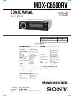
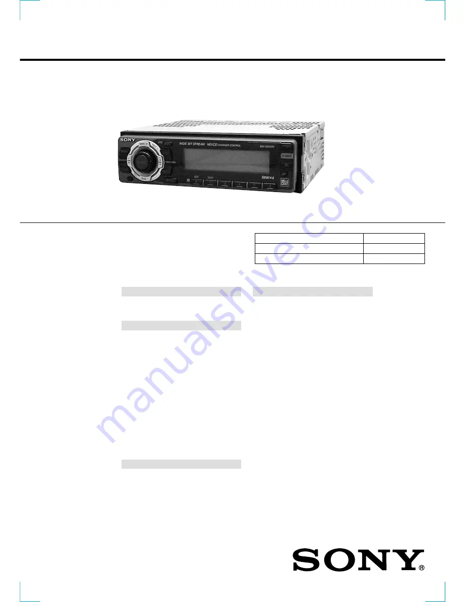
SERVICE MANUAL

AEP Model

UK Model

SPECIFICATIONS

MDX-C6500RV

Model Name Using Similar Mechanism

MDX-C6500R

Base Mechanism Type

MG-164NZ-138

Optical Pick-up Name

KMS-241C/J1NP

FM/MW/LW MINIDISC PLAYER

U.S. and foreign patents licensed from Dolby
laboratories Licensing Corporation.

Design and specifications are subject to change
without notice.

MD player section

Signal-to-noise ratio

90 dB

Frequency response

10 – 20,000 Hz

Wow and flutter

Below measurable limit

Tuner section

FM

Tuning range

87.5 – 108.0 MHz

Aerial terminal

External aerial connector

Intermediate frequency

10.7 MHz/450 kHz

Usable sensitivity

8 dBf

Selectivity

75 dB at 400 kHz

Signal-to-noise ratio

66 dB (stereo),
72 dB (mono)

Harmonic distortion at 1 kHz

0.6 % (stereo),
0.3 % (mono)

Separation

35 dB at 1 kHz

Frequency response

30 – 15,000 Hz

MW/LW

Tuning range

MW: 531 – 1,602 kHz
LW: 153 – 279 kHz

Aerial terminal

External aerial connector

Intermediate frequency

10.7 MHz/450 kHz

Sensitivity

MW: 30 

µ

V

LW: 40 

µ

V

Power amplifier section

Outputs

Speaker outputs
(sure seal connectors)

Speaker impedance

4 – 8 ohms

Maximum power output 50 W 

×

 4 (at 4 ohms)

General

Outputs

Audio outputs
Power aerial relay control
lead
Power amplifier control
lead
Telephone ATT control
lead

Tone controls

Bass 

±

9 dB at 100 Hz

Treble 

±

9 dB at 10 kHz

Power requirements

12 V DC car battery
(negative ground)

Dimensions

Approx. 178 

×

 50 

×

 183 mm

(w/h/d)

Mounting dimensions

Approx. 182 

×

 53 

×

 162 mm

(w/h/d)

Mass

Approx. 1.2 kg

Supplied accessories

Parts for installation and
connections (1 set)
Front panel case (1)

Ver 1.1  2001.05

9-870-087-12

Sony Corporation

2001E0500-1

e Vehicle Company

C

 2001.5

Shinagawa Tec Service Manual Production Group

Summary of Contents for MDX-C6500RV

Page 1: ... stereo 0 3 mono Separation 35 dB at 1 kHz Frequency response 30 15 000 Hz MW LW Tuning range MW 531 1 602 kHz LW 153 279 kHz Aerial terminal External aerial connector Intermediate frequency 10 7 MHz 450 kHz Sensitivity MW 30 µV LW 40 µV Power amplifier section Outputs Speaker outputs sure seal connectors Speaker impedance 4 8 ohms Maximum power output 50 W 4 at 4 ohms General Outputs Audio output...

Page 2: ...ission from right avove when checking it for adustment It is feared that you will lose your sight NOTES ON HANDLING THE OPTICAL PICK UP BLOCK KMS 241C J1NP The laser diode in the optical pick up block may suffer electro static break down easily When handling it perform soldering bridge to the laser tap on the flexible board Also perform m easures against electrostatic break down sufficiently befor...

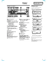
Page 3: ...er buttons During radio reception Preset number select 15 16 18 19 During CD MD playback 1 REP 11 2 SHUF 11 ql AF button 17 18 19 w TA button 18 19 Warning when installing in a car without ACC accessory position on the ignition key switch Be sure to press OFF on the unit for two seconds to turn off the clock display after turning off the engine When you press OFF only momentarily the clock display...

Page 4: ...4 ...

Page 5: ...5 ...

Page 6: ...6 ...

Page 7: ...7 ...

Page 8: ...8 ...

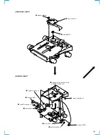
Page 9: ...er given MECHANISM DECK MG 164NZ 138 1 screw PTT2 6 5 4 mechanism deck MG 164NZ 138 2 two screws PTT2 6 5 5 bracket MD 3 connector CN101 1 screw PTT2 6 5 1 screw PTT2 6 5 2 cover 4 claw 3 screw PTT2 6 8 3 two screws PTT2 6 8 3 screw PTT2 6 8 5 sub panel ass y 4 two claws 6 flexible flat cable CN500 ...

Page 10: ...10 SERVO BOARD MAIN BOARD 2 two screws BVTT2 4 1 sensor flexible board CN102 2 two screws BVTT2 4 1 flexible board CN103 3 servo board 1 three ground point screws 2 three screws PTT2 6 8 3 main board ...

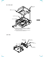
Page 11: ...screwdriver etc disengage the Shaft MD Cover Guide from the slot in the MD Cover Ass y Note Take care not to scratch the optiocal Pick up when pushing the Cassette Holder with a screwdriver etc shaft MD cover guide cassette holder A 1 three screws PTT2 6 8 2 two screws PTT2 6 12 1 screw PTT2 6 8 1 two screws PTT2 6 8 3 heat sink ...

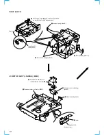
Page 12: ...springs float F 3 Pushing an arrow A part raise the float block up ward at the front to release a lock A float block lever lock R lever lock L 4 Remove the bracket LO in the direction of arrow A bracket LO 1 Remove solders of motor M903 5 LO motor ass y loading M903 2 tension spring rack 3 claw A bottom view ...

Page 13: ...washer 2 lever LE ass y 3 roller gear E 1 2 type E stopring 1 5 2 type E stopring 1 5 3 lever lock L 2 type E stopring 1 5 2 type E stopring 1 5 4 Remove the holder ass y in the direction of the arrow 1 spring CHKG 1 spring CHKG 3 lever lock R ...

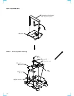
Page 14: ...C J1NP CHUCKING ARM ASS Y 1 Remove the chucking arm ass y in the direction of the arrow holder ass y 6 bearing SL 5 feed screw ass y 3 screw K2 3 2 guide shaft OPT L 1 two screws K2 3 7 optical pick up KMS 241C J1NP 4 screw B2 3 ...

Page 15: ...OR ASS Y SPINDLE M901 4 screw P1 7 1 8 5 bracket SL 9 two screws P1 7 1 8 0 bracket SP qa SP motor ass y spindle M901 7 screw B2 3 2 two screws 2 8 3 sensor board 1 Remove solders of motors M901 M902 8 base SL 6 SL motor ass y sled M902 ...

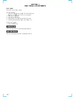
Page 16: ... if the clock is not displayed 2 Push the preset 4 button 3 Push the preset 5 button 4 Press the preset 1 button for more than two seconds 5 Then the display indicates all lights the test mode is set Release the Test mode 1 Push the OFF button MD SECTION MD section adjustments are done automatically in this set TUNER SECTION Tuner section adjustments are done automatically in this set ...

Page 17: ... DECODER PLL FILTER 59 58 61 60 FILI PCO CLTV FILO 100 EFMO 23 ADDT IC301 1 2 15 TX COMPA RATOR 51 52 55 ASYO ASYI RFI ADIP DEMODULATOR DECODER 78 ADFG SPINDLE SERVO 79 F0CNT 94 93 SPFD SPRD SUBCODE PROCESSOR 24 SAMPLING RATE CONVERTER DIGITAL AUDIO INTERFACE 22 21 DIN DOUT DIGITAL SIGNAL PROCESSOR EFM ACIRC ENCODER DECODER SHOCK PROOF MEMORY CONTROLLER ATRAC ENCODER DECODER 2M BIT D RAM IC301 1 2...

Page 18: ...CE REGISTER IIC BUS SLAVE TRANSCEIVER OSCILLATOR CLOCK X51 4 332MHz 4 8 5 OSCI OSCO SDA SCL DAVN 57 kHz BAND PASS FILTER CLOCKED COMPARATOR RDS RDBS DEMODULATOR DECODER SIGNAL QUALITY DECODER 16 18 19 MPX CIN 4 5 SC OUT MULTI PATH DETECTOR 20 2 LVIN MPTH 50 QUALITY 32 NS MASK BAND PASS FILTER IC90 Q90 NOISE DET DISCHARGE SWITCH DATA CLOCK DATA CLOCK Page 19 MPX Page 19 E AM Page 19 F S METER Page ...

Page 19: ...W901 917 S901 904 DIGITAL FILTER D A CONVERTER IC101 INPUT INTERFACE DIGITAL FILTER NOISE SHAPER D A COMVERTER 4 DEMODULATOR 21 70 71 18 LEVEL 14 57 MUTING Q181 MUTING Q271 MUTING Q171 62 63 BATTERY OFF MUTE DRIVER Q621 BACK UP B D622 D502 D302 X501 3 68MHz X502 32 768kHz RESET RESET EMPHASIS I H C INPUT MULTIPLEXER LOUDNESS MUTE MONO FADER MIXER OUTLF OUTLR R CH OUTPUT SELECTOR AM FM NOISE BLANKE...

Page 20: ...OL SWITCH Q633 FU601 COM 8V AUDIO CIRCUIT B 05 RST 3 BATT BATTERY SWITCH 10 BU IN UNISI 50 UNISO UNICKIO MDMON 10 77 3 19 UNICKO 17 UNISI 18 UNISO 86 HSTX 11 24 SIRCS 90 65 MD ON D301 D708 TH701 D702 D701 D662 LED810 LSW810 LED810 MD DISC SLOT VCC TUNER 5 6V RDS DECODER IC51 B TUNER 8 7V VCC 7 7 ACC REGULATOR Q631 12V REGULATOR Q361 3 3V REGULATOR IC401 Q401 5V REGULATOR Q362 B SWITCH Q402 403 3 3...

Page 21: ...chematic Diagram All capacitors are in µF unless otherwise noted pF µµF 50 WV or less are not indicated except for electrolytics and tantalums All resistors are in Ω and 1 4 W or less unless otherwise specified indicates tolerance f internal component C panel designation U B Line Power voltage is dc 14 4V and fed with regulated dc power supply from ACC and BATT cords Voltages are taken with a VOM ...

Page 22: ... C352 R518 R516 R511 R532 R527 C327 C329 C326 C325 R347 R355 R345 R340 R336 C321 R343 R344 R342 R338 R528 R526 R529 R501 R502 R503 R531 R535 R539 R506 R507 C11 C108 R319 R317 R312 R316 FB301 FB302 R102 R538 R525 R524 R523 R530 R522 R537 R536 C516 R504 C501 R505 C328 C331 R356 C330 R346 R341 R339 C347 C320 R348 C322 R337 R357 R349 C324 R517 R404 C402 R405 R311 R308 R307 R306 R305 R302 R353 C343 C34...

Page 23: ...351 TH501 C307 C357 C356 C301 C358 C512 C316 C350 C333 C503 C510 R539 R101 C101 R201 C201 C309 C317 C302 C353 C345 C359 R401 R402 R403 R104 R202 R335 R333 R334 R332 R534 R533 R519 R521 R520 R542 R540 R512 R510 1 A 2 3 4 5 6 7 8 9 B C D E F G H I 4 7 PRINTED WIRING BOARD SERVO Board Conductor Side See page 21 for Circuit Boards Location Semiconductor Location Ref No Location IC307 C 8 Q402 B 4 Q403...

Page 24: ...ms See page 36 for IC Block Diagrams Voltages and waveforms are dc with respect to ground under no signal conditions no mark MD PLAY Impossible to measure The components identified by mark 0 or dotted line with mark 0 are critical for safety Replace only with part number specified ...

Page 25: ...9 SCHEMATIC DIAGRAM SERVO Board 2 2 See page 31 for Waveforms See page 36 for IC Block Diagrams Voltages and waveforms are dc with respect to ground under no signal conditions no mark MD PLAY Impossible to measure Page 29 ...

Page 26: ...5 D662 D 5 D673 C 5 D674 C 5 D701 E 5 D702 C 4 D703 B 3 D704 B 2 D705 B 2 D706 B 2 D708 G 7 D710 D 4 IC51 I 12 IC90 G 11 IC151 D 10 IC501 I 5 IC652 J 3 IC701 C 3 Q1 G 11 Q111 E 12 Q131 F 12 Q171 B 11 Q181 B 11 Q250 H 2 Q271 C 11 Q281 C 11 Q363 I 3 Q551 J 6 Q571 D 5 Q621 C 10 Q622 C 9 Q633 J 2 Q651 I 8 Q652 I 8 Q661 D 5 Q701 D 5 Q704 G 7 Q705 C 4 Q706 D 4 4 10 PRINTED WIRING BOARD MAIN Board Compon...

Page 27: ...76 I 4 D677 I 4 D709 G 5 IC611 A 7 IC671 F 1 Q90 G 11 Q121 E 12 Q361 H 1 Q362 G 1 Q631 J 2 Semiconductor Location Ref No Location 4 11 PRINTED WIRING BOARD MAIN Board Conductor Side See page 21 for Circuit Boards Location 5 4 8 7 6 2 1 3 FRONT VIEW 9 10 11 12 13 14 15 16 1 2 3 4 5 6 7 8 RL FL FR RL FR BATT GND BATT RR RL FL RL FL FR RR FL RL RR FR ANT REM AMP REM ACC ACC ANT REM GND ATT Page 32 Pa...

Page 28: ... 4 12 SCHEMATIC DIAGRAM MAIN Board 1 3 See page 31 for Waveforms See page 36 for IC Block Diagrams Voltages and waveforms are dc with respect to ground under no signal detuned conditions no mark FM MW LW Page 29 Page 30 ...

Page 29: ...oltages and waveforms are dc with respect to ground under no signal detuned conditions no mark FM MW LW MD PLAY Impossible to measure 4 13 SCHEMATIC DIAGRAM MAIN Board 2 3 See page 31 for Waveforms Page 25 Page 28 Page 30 ...

Page 30: ...X C6500RV 30 30 4 14 SCHEMATIC DIAGRAM MAIN Board 3 3 See page 36 for IC Block Diagrams Voltages are dc with respect to ground under no signal detuned conditions no mark FM MD PLAY Page 29 Page 28 Page 33 ...

Page 31: ...de qd IC304 3 MD Play Mode qf IC304 7 MD Play Mode qg IC501 ea EXTAL 6 IC301 wh XBCK MD Play Mode 4 4 Vp p 88 ns 4 6 Vp p 354 ns Apporx 0 6 Vp p 3 8 Vp p 22 7 µs 4 4 Vp p 88 ns 3 4 Vp p 354 ns Apporx 1 5 Vp p 4 IC301 qh OSCI MD Play Mode 5 IC301 wg LRCK MD Play Mode 4 6 Vp p 44 3 ns 4 4 Vp p 22 7 µs Approx 0 5 Vp p Approx 2 Vp p 4 1 Vp p 44 3 ns 3 4 Vp p 44 3 ns 4 4 Vp p 44 3 ns 3 7 Vp p 101 ns MA...

Page 32: ...MDX C6500RV 32 32 4 15 PRINTED WIRING BOARD SUB Board See page 21 for Circuit Boards Location Page 27 Page 34 ...

Page 33: ...MDX C6500RV 33 33 4 16 SCHEMATIC DIAGRAM SUB Board Page 30 ...

Page 34: ...ocation Component Side Ref No Location IC951 C 5 LED901 A 2 LED902 C 2 LED903 C 3 LED904 A 3 LED910 B 12 LED911 B 12 LED912 A 12 LED913 A 5 LED914 B 5 LED915 B 5 Semiconductor Location Conductor Side Ref No Location D901 A 11 D902 B 10 D903 B 10 D904 B 10 D951 C 4 D952 B 6 IC901 B 8 Q903 A 5 Q903 B C E Page 32 ...

Page 35: ...MDX C6500RV 35 35 4 18 SCHEMATIC DIAGRAM KEY Board See page 31 for Waveforms Voltages and waveforms are dc with respect to ground under no signal detuned conditions no mark FM Page 33 ...

Page 36: ...8 XTSL 17 OSCO 16 OSCI 15 TX 14 XINT 13 RECP 12 DQSY 11 SQSY 10 XRST 9 SENS 8 SRDT 7 XLAT 6 SCLK 5 SWDT 4 MNT3 3 MNT2 2 MNT1 1 MNT0 PWM GENERATOR AUTO SEQUENCER SERVO DSP CPU I F MONITOR CONTROL SPINDLE SERVO EACH BLOCK EACH BLOCK DIGITAL AUDIO I F SAMPLING RATE CONVERTER CLOCK GENERATOR SUBCODE PROCESSOR EACH BLOCK A D CONVERTER ANALOG MUX EFM ACIRC ENCODER DECODER PLL SHOCK RESISTANT MEMORY CONT...

Page 37: ...PREDRIVE AMP INTERFACE AMP AMP AMP VDD PSB AMP 1 2 3 4 OUT1 VM VCC FIN 8 7 6 5 GND OUT2 VREF RIN CONTROL LOGIC TSD POWER SAVE DRIVER DRIVER IC307 MN41V4400TT 08S DATA BUS DQ3 DQ4 VSS 3 DQ2 2 A9 5 A0 9 A1 10 A2 11 A3 12 VCC 13 NC 6 NC 7 NC 8 DQ1 1 26 23 24 25 A8 NC NC NC 19 20 21 A6 A7 17 18 A4 A5 15 14 16 ROW DECODERS WORD DRIVERS MEMORY CELLS INTERNAL ADDRESS COUNTER TIMING GENERATOR TIMING GENER...

Page 38: ... POWER SUPPLY RESET TEST CONTROL OSCILLATOR CLOCK PAUSE DETECTOR MULTI PATH DETECTOR 57kHz 8th ORDER BAND PASS FILTER RDS RDBS DECODER RDS RDBS DEMODULATOR IIC BUS SLAVE TRANSCEIVER 17 18 CIN 19 LVIN 20 8 7 DATA CLOCK DATA CLOCK 4 4 5 9 10 3 4 5 IC671 BA4908 V3 OVER VOLTAGE PROTECT REGULATOR 1 2 3 4 5 6 7 8 9 10 12 11 NC TUNER8 7 ANT SW TUNER5 6 SW STB VDD5 6V AMP VCC ANT COM8 7V TUNER5 6V TUNER8 ...

Page 39: ...TOR D A CONVERTER PILOT CANCELATION PIL DET PLL AM FM NOISE BLANKER BEEP 80kHz LP 17 PULSE FORMER QUAL SUPPLY SECOND MAIN ACIN MONO FADER MONO FADER MONO FADER MONO FADER MONO FADER MONO FADER SUBWOOFER PHASE CONTROL MIXER OUTPUT SELECTOR FRONT REAR SW VDD SCL SDA GND SM QUAL MPOUT MPIN LEVEL MPX AMIF SEL SER FD1L FD1L FD1R FD1R FD2L FD2L FD2R FD2R AM ACINLF SWINR SWINL ACOUTR ACOUTL CREF MUX MD1 ...

Page 40: ...tic head on off output Not used fixed at L 16 OSCI I System clock signal 512Fs 22 5792 MHz input from the oscillator circuit 17 OSCO O System clock signal 512Fs 22 5792 MHz output terminal Not used open 18 XTSL I Input terminal for the system clock frequency setting L 45 1584 MHz H 22 5792 MHz fixed at H in this set 19 RVDD Power supply terminal 3 3V digital system 20 RVSS Ground terminal digital ...

Page 41: ...e CXA2523AR IC302 68 ADIO O A Monitor output of the A D converter input signal Not used open 69 AVDD Power supply terminal 3 3V analog system 70 ADRT I A A D converter operational range upper limit voltage input terminal fixed at H in this set 71 ADRB I A A D converter operational range lower limit voltage input terminal fixed at L in this set 72 AVSS Ground terminal analog system 73 SE I A Sled e...

Page 42: ... signal output to the BH6511FS IC303 93 SPRD O Spindle servo drive PWM signal output to the BH6511FS IC303 94 SPFD O Spindle servo drive PWM signal output to the BH6511FS IC303 95 FGIN I Not used fixed at L 96 TEST1 I 97 TEST2 I Input terminal for the test fixed at L 98 TEST3 I 99 DVSS Ground terminal digital system 100 EFMO O EFM signal output terminal when recording mode Not used open I A for an...

Page 43: ...l circuit BPF3T 24 VCC Power supply terminal 3 3V 25 WBLADJ I Center frequency setting terminal for the internal circuit BPF22 26 TE O Tracking error signal output to the CXD2652AR IC301 27 CSLED I Connected to the external capacitor for low pass filter of the sled error signal 28 SE O Sled error signal output to the CXD2652AR IC301 29 ADFM O FM signal output of the ADIP 30 ADIN I Receives a ADIP ...

Page 44: ... 4M bit external D RAM H 2M bit internal D RAM of CXD2652AR fixed at L in this set 24 25 NCO O Not used open 26 MNT0 I Focus OK signal input from the CXD2652AR IC301 H is input when focus is on L NG 27 MNT1 I Track jump detection signal input from the CXD2652AR IC301 28 MNT2 I Busy monitor signal input from the CXD2652AR IC301 29 MNT3 I Spindle servo lock status monitor signal input from the CXD26...

Page 45: ...he SONY bus interface IC701 and battery check circuit H battery on 61 BUS ON I SONY bus on off control signal input from the master controller IC501 L bus on 62 SQSY I Subcode Q sync SCOR input from the CXD2652AR IC301 L is input every 13 3 msec Almost all H is input 63 C SW I Inputs the disc loading start or disc eject completion detect switch detection signal L When start or eject completed of t...

Page 46: ...l data input from the SONY bus interface IC701 18 UNISO O Serial data output to the SONY bus interface IC701 19 UNICKO O Serial clock signal output to the MD mechanism controller IC501 and SONY bus interface IC701 20 UNICKI I Serial clock signal input from the MD mechanism controller IC501 for SONY bus 21 CD MD I Setting terminal for the internal mechanism CD or MD L CD H MD fixed at H in this set...

Page 47: ... muting on off control signal output terminal H muting on 59 AMPON O Standby on off control signal output to the power amplifier IC611 L standby mode H ampifier on 60 AMPATT O Power amplifier muting on off control signal output to the power amplifier IC611 L muting on 61 COLSW I Setting terminal for the illumination color L 2 color H 1 color fixed at H in this set 62 COLSEL I Setting terminal for ...

Page 48: ...ion signal input terminal L auto metal Not used open 103 AMS IN I Input terminal of whether a music is present or not is detected at auto music sensor L music is present H music is not present Not used open 104 REEL I Rotation detect signal input terminal Not used open 105 POS0 I 106 POS1 I 107 POS2 I 108 POS3 I 109 LM EJ O Loading motor control signal output terminal H active For the eject direct...

Page 49: ...iption 117 TAPATT O Audio signal select control signal output terminal Not used open 118 NCO O Not used open 119 VSS Ground terminal 120 PW ON O Main system power supply on off control signal output to the BA4908 IC671 H power on ...

Page 50: ...ference from the original one Color Indication of Appearance Parts Example KNOB BALANCE WHITE RED Parts Color Cabinet s Color Ref No Part No Description Remark Ref No Part No Description Remark 1 X 3378 458 1 PANEL ASSY SUB 2 X 3376 699 2 GEAR ASSY 3 3 030 909 02 DAMPER OIL 4 3 713 786 51 SCREW P 2X3 5 3 034 086 01 SPRING DOOR 6 3 033 750 02 DOOR MD 7 3 040 990 01 BUTTON EJECT Z 8 1 677 057 11 SUB...

Page 51: ...BUTTON LIST ENTER DSPL LIST ENTER 55 3 040 980 01 BUTTON SOURCE 56 3 040 981 01 KNOB VOL 59 3 040 997 01 PLATE LCD GROUND 60 1 694 660 11 CONDUCTIVE BOARD CONNECTION 61 3 041 371 01 SHEET REFLECTOR 62 3 040 993 01 PLATE LCD LIGHT GUIDE 63 3 040 992 01 HOLDER LCD 64 X 3378 398 1 PANEL ASSY FRONT BACK 65 3 935 151 01 SPRING OPEN 66 3 040 989 01 BUTTON OPEN 67 3 041 005 11 BUTTON D D BASS 68 3 041 00...

Page 52: ...714 02 SPRING FLOAT F TENSION 104 3 921 111 01 SPRING FLOAT B TENSION 105 3 919 273 01 DAMPER OIL 106 X 3376 796 3 HOLDER ASSY 107 3 032 682 01 SPRING HOLDER 108 3 034 301 01 CUSHION EJ2 109 3 034 302 01 CUSHION EJ3 110 3 032 712 01 LEVER LOCK R 111 3 919 281 01 SPRING CHUCKING 112 X 3376 800 1 COVER ASSY MD 113 3 035 932 01 WASHER STOPPER 114 X 3376 797 3 LEVER LE ASSY 115 3 032 707 01 SPRING LEV...

Page 53: ...ark Ref No Part No Description Remark 161 X 3373 213 1 SCREW ASSY FEED 162 3 939 590 07 SCREW IB LOCK 163 3 010 091 01 SPRING SL FEED 164 3 919 293 01 SHAFT OPT S GUIDE 0165 8 583 065 03 OPTICAL PICK UP KMS 241C J1RP 166 3 920 537 01 SHAFT OPT L GUIDE M901 A 3301 407 A MOTOR ASSY SP SPINDLE M902 A 3291 190 A MOTOR ASSY SL SLED M903 A 3291 191 A MOTOR ASSY LO LOADING M902 M901 M903 7 7 8 9 9 8 157 ...

Page 54: ...ON LED902 8 719 061 16 LED CL 190SR CD T ILLUMINATION LED903 8 719 061 16 LED CL 190SR CD T ILLUMINATION LED904 8 719 061 16 LED CL 190SR CD T ILLUMINATION LED910 8 719 072 40 LED LBA676 J2K1K2 LCD BACK LIGHT LED911 8 719 072 40 LED LBA676 J2K1K2 LCD BACK LIGHT LED912 8 719 072 40 LED LBA676 J2K1K2 LCD BACK LIGHT LED913 8 719 072 40 LED LBA676 J2K1K2 LCD BACK LIGHT LED914 8 719 072 40 LED LBA676 J...

Page 55: ...6V C13 1 163 017 00 CERAMIC CHIP 0 0047uF 5 50V C14 1 163 021 11 CERAMIC CHIP 0 01uF 10 50V C52 1 164 004 11 CERAMIC CHIP 0 1uF 10 25V C53 1 163 229 11 CERAMIC CHIP 12PF 5 50V C54 1 163 229 11 CERAMIC CHIP 12PF 5 50V C55 1 164 004 11 CERAMIC CHIP 0 1uF 10 25V C56 1 124 589 11 ELECT 47uF 20 16V C57 1 164 004 11 CERAMIC CHIP 0 1uF 10 25V C58 1 163 263 11 CERAMIC CHIP 330PF 5 50V C59 1 164 505 11 CER...

Page 56: ...2uF 25V C632 1 164 222 11 CERAMIC CHIP 0 22uF 25V C641 1 162 964 11 CERAMIC CHIP 0 001uF 10 50V C653 1 163 021 11 CERAMIC CHIP 0 01uF 10 50V C654 1 125 710 11 DOUBLE LAYER 0 1F 5 5V C655 1 124 584 00 ELECT 100uF 20 10V C661 1 109 982 11 CERAMIC CHIP 1uF 10 10V C671 1 126 157 11 ELECT 10uF 20 16V C672 1 126 157 11 ELECT 10uF 20 16V C673 1 126 157 11 ELECT 10uF 20 16V C674 1 124 233 11 ELECT 10uF 20...

Page 57: ...C50 1 216 295 00 SHORT 0 JC54 1 216 295 00 SHORT 0 JC90 1 216 295 00 SHORT 0 JC191 1 216 295 00 SHORT 0 JC192 1 216 295 00 SHORT 0 JC193 1 216 295 00 SHORT 0 JC194 1 216 295 00 SHORT 0 JC301 1 216 864 11 SHORT 0 JC601 1 216 864 11 SHORT 0 JC671 1 216 295 00 SHORT 0 JC673 1 216 864 11 SHORT 0 COIL L601 1 419 476 11 INDUCTOR 250uH L671 1 410 989 11 INDUCTOR CHIP 0 47uH TRANSISTOR Q1 8 729 120 28 TRA...

Page 58: ...24 1 216 073 00 METAL CHIP 10K 5 1 10W R525 1 216 073 00 METAL CHIP 10K 5 1 10W R526 1 216 097 00 RES CHIP 100K 5 1 10W R529 1 216 049 11 RES CHIP 1K 5 1 10W R531 1 216 839 11 METAL CHIP 33K 5 1 16W R532 1 216 833 11 RES CHIP 10K 5 1 16W R533 1 216 833 11 RES CHIP 10K 5 1 16W R534 1 216 097 00 RES CHIP 100K 5 1 10W R535 1 216 845 11 METAL CHIP 100K 5 1 16W R537 1 216 097 00 RES CHIP 100K 5 1 10W R...

Page 59: ...C320 1 164 227 11 CERAMIC CHIP 0 022uF 10 25V C321 1 162 969 11 CERAMIC CHIP 0 0068uF 10 25V C322 1 162 964 11 CERAMIC CHIP 0 001uF 10 50V C324 1 107 826 11 CERAMIC CHIP 0 1uF 10 16V C325 1 110 563 11 CERAMIC CHIP 0 068uF 10 16V C326 1 162 968 11 CERAMIC CHIP 0 0047uF 10 50V C327 1 109 982 11 CERAMIC CHIP 1uF 10 10V C328 1 162 966 11 CERAMIC CHIP 0 0022uF 10 50V C329 1 164 227 11 CERAMIC CHIP 0 02...

Page 60: ...16 1 216 821 11 METAL CHIP 1K 5 1 16W R317 1 216 809 11 METAL CHIP 100 5 1 16W R318 1 216 833 11 RES CHIP 10K 5 1 16W R319 1 216 845 11 METAL CHIP 100K 5 1 16W R320 1 216 855 11 METAL CHIP 680K 5 1 16W R324 1 216 827 11 METAL CHIP 3 3K 5 1 16W R325 1 216 821 11 METAL CHIP 1K 5 1 16W R327 1 216 821 11 METAL CHIP 1K 5 1 16W R328 1 216 811 11 METAL CHIP 150 5 1 16W R329 1 216 819 11 METAL CHIP 680 5 ...

Page 61: ...T CONNECTOR 14P CNP811 1 792 195 11 CABLE FLEXIBLE FLAT DIODE D806 8 719 109 97 DIODE MA4068 M TA D810 8 719 056 82 DIODE UDZ TE 17 6 2B D811 8 719 056 82 DIODE UDZ TE 17 6 2B D812 8 719 056 82 DIODE UDZ TE 17 6 2B D813 8 719 056 82 DIODE UDZ TE 17 6 2B D814 8 719 056 82 DIODE UDZ TE 17 6 2B LED LED810 8 719 077 75 LED BR1101F TR MD DISC SLOT SWITCH LSW810 1 771 883 21 SWITCH TACTILE WITH LED Z MI...

Page 62: ...2 505 506 503 SCREW FITTING 1 BUSHING 1 507 POWER CORD 1 PARTS FOR INSTALLATION AND CONNECTION 501 1 465 459 21 ADAPTER ANTENNA 502 3 012 360 31 FRAME 503 3 040 979 01 COLLAR 504 3 233 644 01 SPRING FITTING 505 3 934 325 01 SCREW K 5X8 TAPPING 506 X 3366 405 1 SCREW ASSY EXP FITTING 507 1 776 527 61 CORD WITH CONNECTOR ISO POWER 504 Ver 1 1 2001 05 ...

Page 63: ...63 MDX C6500RV MEMO ...

Page 64: ...ows you to jump to the revised page Also clicking the version at the upper right on the revised page allows you to jump to the next revised page Ver Date Description of Revision 1 1 2001 05 Change of Part No for SPRING FITTING ECN CSA04727 1 0 2000 03 New ...

Reviews: