background image

SERVICE MANUAL

PORTABLE MINIDISC PLAYER

E Model

Tourist Model

SPECIFICATIONS

MZ-E800

US and foreign patents licensed from Dolby
Laboratories Licensing Corporation.

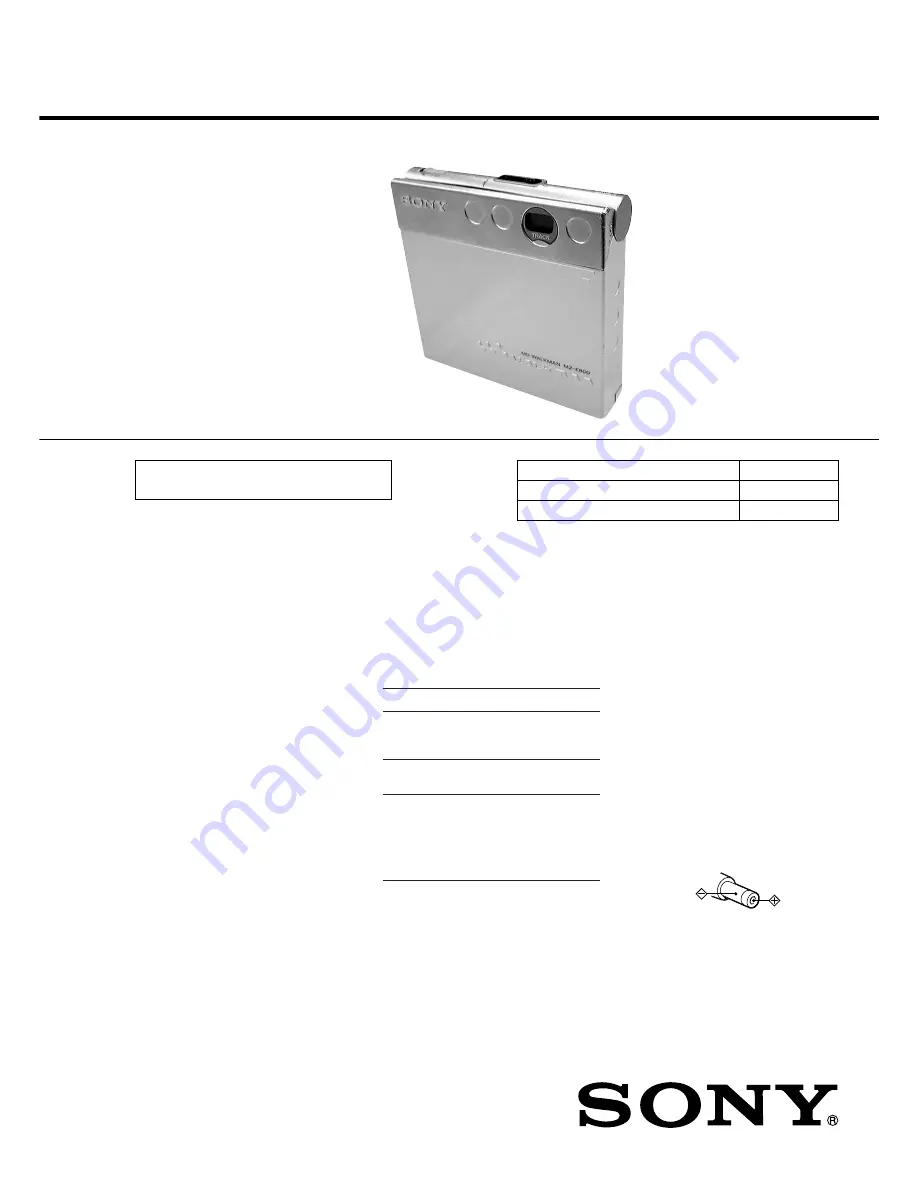
Photo: Silver type

Model Name Using Similar Mechanism

NEW

MD Mechanism Type

MT-MZE800-170

Optical Pick-up Mechanism Type

LCX-2E

System

Audio playing system

MiniDisc digital audio system

Laser diode properties

Material: GaAlAs
Wavelength: 

λ

 = 790 nm

Emission duration: continuous
Laser output: less than 44.6 

µ

W*

* This output is the value measured at a distance

of 200 mm from the objective lens surface on
the optical pick-up block with 7 mm aperture.

Revolutions

600 rpm to 2250 rpm

Error correction

Advanced Cross Interleave Reed Solomon Code
(ACIRC)

Sampling frequency

44.1 kHz

Coding

Adaptive TRansform Acoustic Coding (ATRAC)

Modulation system

EFM (Eight to Fourteen Modulation)

Number of channels

2 stereo channels
1 monaural channel

Frequency response

20 to 20,000 Hz 

±

 3 dB

Wow and Flutter

Below measurable limit

Outputs

Earphones: stereo mini-jack, maximum output
level 5 mW + 5 mW, load impedance 16 ohms

General

Power requirements

Nickel metal hydride rechargeable battery
One NH-14WM (supplied): 1.2V,  1,400 mAh
One LR6 (size AA) battery (not supplied)
Sony AC Power Adaptor* (supplied) connected
to the DC IN 3V jack

Battery operation time

Dimensions

Approx. 79.5 

×

 76.7 

×

 17.0 mm (w/h/d) (not

including projecting parts and controls)

Mass

Approx. 110g (the player only)

Supplied accessories

Earphones with a remote control (1)
Charging stand (1)
Nickel metal hydride rechargeable battery (1)
AC power adaptor (1)
Dry battery case (1)
Rechargeable battery carrying case (1)
Carrying pouch (1)

Design and specifications are subject to change
without notice.

Playback

Approx. 24 hours*

Approx. 37 hours

Approx. 64 hours

Battery life

*

Batteries

Ni-MH
rechargeable battery
(NH-14WM)

One (size AA)
alkaline battery**

One (size AA)
alkaline battery**
and a Ni-MH
rechargeable
battery
(NH-14WM)

* With a fully charged battery

** When using a LR6 (SG) Sony “STAMINA”

alkaline dry battery (produced in Japan).

Note

The battery life may be shorter depending on
operating conditions, the surrounding
temperature, and the battery type.

About power sources

• For use in your house or car: Use the

supplied AC power adaptor or the
DCC-E230 car battery cord (not supplied)
to supply power to the player.  Do not use
any other power supply.

Polarity of the plug

Ver 1.1  2001.02

9-927-939-12

Sony Corporation

2001B0500-1

Audio Entertainment Group

C

 2001.2

General Engineering Dept.

Summary of Contents for MZ-E800

Page 1: ...ttery One NH 14WM supplied 1 2V 1 400 mAh One LR6 size AA battery not supplied Sony AC Power Adaptor supplied connected to the DC IN 3V jack Battery operation time Dimensions Approx 79 5 76 7 17 0 mm w h d not including projecting parts and controls Mass Approx 110g the player only Supplied accessories Earphones with a remote control 1 Charging stand 1 Nickel metal hydride rechargeable battery 1 A...

Page 2: ...ing By connecting an optional car battery cord to the battery charger you can listen to the player in the car without worrying about battery rundown LCD display built into player for easy viewing in the car An easy to see LCD display built into the player allows you to monitor track numbers when the remote control display is out of view Personalized sound through Digital Sound Preset functions You...

Page 3: ...n easily When handling it perform soldering bridge to the laser tap on the flexible board Also perform mea sures against electrostatic break down sufficiently before the op eration The flexible board is easily damaged and should be handled with care OPTICAL PICK UP FLEXIBLE BOARD SECTION 1 SERVICING NOTES In performing the repair with the power supplied to the set removing the MAIN board causes th...

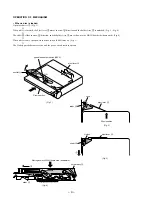
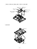
Page 4: ...PERATION OF MECHANISM When a disc is loaded Open the shutter 1 Fig 1 j When a disc is inserted the Eject lever 2 moves in arrow direction and the holder Assy 3 is unlocked Fig 1 Fig 4 j The slider 4 slides in arrow direction and the holder Assy 3 moves down to the MAIN board side downward Fig 4 j When a disc lowers the open close detect switch S809 turns on Fig 1 j The Wake up mode becomes active ...

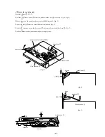
Page 5: ...l block 4 moves in arrow direction inward Fig 5 j The disc 6 is pushed out by the Eject lever 5 and ejected from the holder Assy 3 Fig 7 j The Sleep mode becomes active and the power supply stops a b b open close detect switch S809 eject lever 5 shutter 1 Disc ejection 6 OFF Fig 5 optical block 4 a eject lever 5 Unlock slider 2 Fig 6 eject lever 5 Lock slider 2 Disc ejection 6 Fig 7 a slider 2 Fig...

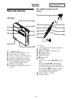
Page 6: ... Earphones Can be replaced with optional earphones 2 Stereo mini plug 3 HOLD Locking the control switch 4 X pause button 5 PLAYMODE button 6 DISPLAY button 7 x stop button 8 Control To play press towards N during stop Press towards N during play to search the beginning of the succeeding track hold in this position to fast foward Press towards during play to search the beginning of the preceding tr...

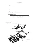
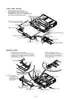
Page 7: ...al LCD901 Main Board OP Service Assy LCX 2E Motor DC SSM17A C NP Spindle M901 Motor DC Sled M902 Holder Assy 2 claw 3 lid battery case holder assy LCD flexible board 4 two MI screws 1 4 5 panel assy rear 4 two MI screws 1 4 1 Open the battery case lid Note In removing or mounting the rear panel insert a disc into the mechanism deck so as to keep the holder Assy in down position Note In mounting th...

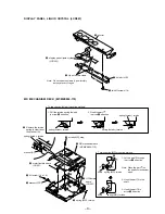
Page 8: ...very fragile and require careful handling A B C Note Do not apply an excessive force when removing an adhesive sheet FPC from the bracket FPC LCD flexible board mounting method Meeting with the screw holes 2 pcs and claws 4 pcs mount the LCD flexible board and bend it into S shape before the connector CN801 and then fix with the sheet flexible as shown in the figure sheet flexible screw 6 screw st...

Page 9: ... arrow B direction 1 Pull the torsion spring holder in arrow A direction A spring holder torsion B a a Torsion spring MD mounting method 1 Let the part through in arrow C direction Note Place the part on the shaft of mechanism deck 2 Hook the part to the shaft 3 Hook the part in arrow D direction shaft spring MD torsion C D b d c b b c d DISPLAY PANEL LIQUID CRYSTAL LCD901 MD MECHANISM DECK MT MZE...

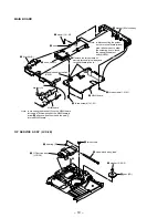
Page 10: ... the bracket A on the MAIN board let the part through under the MAIN board in arrow A direction and then insert the part into the MAIN board Note In disconnecting the solder on the terminal board minus side take care not to allow the soldering iron to touch the open close detect switch S809 1 three screws 1 4 MI A a b a b MAIN BOARD OP SERVICE ASSY LCX 2E 5 bearing N 7 OP service assy LCX 2E 3 two...

Page 11: ...C SSM17A C NP SPINDLE M901 MOTOR DC SLED M902 HOLDER ASSY 4 motor DC sled M902 3 three screws M1 4 5 motor DC SSM17A C NP spindle M901 3 two screws M1 4 1 washer 0 8 2 5 2 gear SA 3 holder assy 1 washer 0 8 2 5 2 ...

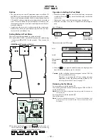
Page 12: ...NV reset see page 17 Releasing the Test Mode For test mode set with the method 1 Turn off the power and open the solder bridge on TAP801 TEST on the MAIN board Note Remove the solders completely Remaining could be shorted with the chassis etc For test mode set with the method 2 Turn off the power Note If electrical adjustment see page 17 has not been finished com pletely always start in the test m...

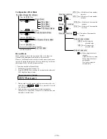
Page 13: ...nual Mode Servo Mode Audio Mode Power Mode OP Alignment Mode Overall Adjustment Mode Self Diagnosis Display Mode Press the VOL key Key Check Mode Test Mode Display Check Mode Press the x key Press the x key Press the x key Press the or VOL key press the DISPLAY key Press the DISPLAY key for several seconds about 3 seconds Quit the key check Remote commander LCD display 000 M a n u a l VOL key 100t...

Page 14: ...ual mode and press the x key to return to the test mode display check mode Overall Adjustment Mode Mode to adjust the servo automatically in all items Normally automatic adjustment is executed in this mode at the repair For further information refer to Section 5 ElectricalAdjustments see page 17 Address Adjusted Value Display Remote commander LCD display Jitter Value Adjusted Value Display Remote ...

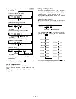
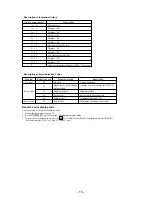
Page 15: ... reset the error display code 1 Setting the test mode see page 12 2 Press the DISPLAY key activates the self diagnosis display mode 3 To reset the error display code press the X key 2 times when the code is displayed except R 0000 All the data on the 1st N N 1 and N 2 will be reset Problem Indication code Meaning of code Description No error 00 No error Normal condition 01 Illegal access target ad...

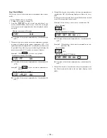
Page 16: ...key for several seconds about 3 sec onds activates the key check mode At the last two digits AD value of remote commander key line is displayed in hexa decimal AD value of the remote commander key hexadecimal 00 to FF 3 When each key on the set and on remote commander is pressed its name is displayed on the remote commander LCD The operated position is displayed for 4 seconds after the slide switc...

Page 17: ...tem number 036 see page 13 2 Press the X key The item number changes to 762 when X key is pressed NV Reset Caution On the set having the microcomputer version 1 000 the NV reset failure will occur Therefore in executing the NV reset during electrical adjustment follow the troubleshooting method of NV reset to perform the NV reset Setting method of NV reset 1 Select the manual mode of the test mode...

Page 18: ... the TP918 VC on the MAIN board and adjust VOL key voltage up or VOL key voltage down so that the voltage becomes 2 305 V 2 Press the X key to write the adjusted value The item number changes to 764 when X key is pressed Adjustment and Connection Location MAIN board see page 19 Adjustment method of Vrem PWM Duty L item number 764 1 Connect a digital voltmeter to the TP919 VR on the MAIN board and ...

Page 19: ...pressing the X key 3 Press the X key to write the adjusted value Adjustment method of trickle charging current item number 722 1 Select the manual mode of the test mode and set item number 722 see page 13 2 Connect a digital voltmeter between TP901 BATT and TP902 BATT on the MAIN board and adjust with VOL key voltage up or VOL key voltage down so that the voltage becomes 0 168 V If the voltage is ...

Page 20: ...LER ATRAC ENCODER DECODER D A CONVERTER 16M BIT D RAM IC601 1 2 PEAK BOTM ABCD FE TE VC MNT2 XRST ADIP APCREF RF AMP FOCUS TRACKING ERROR AMP IC501 AUTOMATIC POWER CONTROL Q501 20 LD SERIAL INTERFACE 22 13 2 23 24 15 18 17 BEEP BEEP STB MUTE BEEP OUT B BEEP OUT A OUT L OUT R IN L IN R VREF IN REFERENCE VOLTAGE SWITCHING Q301 21 4 HEADPHONE AMP IC301 52 22 23 18 85 19 54 12 13 28 11 33 53 55 29 39 ...

Page 21: ...IGNAL PROCESSOR DIGITAL SERVO SIGNAL PROCESSOR EFM ACIRC ENCODER DECODER SHOCK PROOF MEMORY CONTROLLER ATRAC ENCODER DECODER D A CONVERTER 16M BIT D RAM IC601 2 2 SLCV SLCU OSCI TFDR OSCO TRDR SPDV SPDW FRDR SLDV SLDU SLVS SLDW SLCW SPCW SPCV SPCU FFDR X601 22 5792MHz X801 16 9344MHz M902 SLED M901 SPINDLE 05 32 7 11 37 38 39 40 BIAS 5 M M A FO3 FO4 RO4 UO VO WO RO3 FO2 COM CPW1 CPV1 CPU1 FO1 RO1 ...

Page 22: ...GE CONTROL IC901 1 2 Q903 CHARGE MONITOR IC901 2 2 VRM RF AMP IC501 DSP IC601 B DSP IC601 REMOTE COMMANDER B DSP IC601 1 7V B SWITCH Q912 1 7V REGULATOR IC902 B SWITCH Q803 VC B VG MOTOR COIL DRIVE IC551 B BATT B VRM B SWITCHING Q911 B SWITCH Q904 CHARGE ON OFF SWITCH Q902 DC DC CONVERTER D904 L903 Q910 DC DC CONVERTER D902 IC903 L901 DC IN DETECT SWITCH Q901 RELAY DRIVE Q913 Q915 RY901 BATT HEADP...

Page 23: ...2 61 62 63 24 23 22 66 65 64 20 21 19 67 68 69 18 17 16 70 71 72 15 14 13 73 75 74 12 11 10 76 77 78 9 8 7 79 80 81 5 6 4 82 84 83 3 2 115 112 111 106 103 100 97 94 91 85 86 1 118 116 114 110 107 104 101 98 95 92 89 87 120 119 117 113 109 108 105 102 99 96 93 90 88 C606 L501 Q301 B C E R301 R302 C852 C853 C854 R206 R201 R101 R106 C351 D201 K A C305 R203 D101 A K C203 R103 C301 R207 R941 E C B Q901...

Page 24: ...ated dc power supply from battery terminal Voltages and waveforms are dc with respect to ground in playback mode no mark PLAYBACK Impossible to measure Voltages are taken with a VOM Input impedance 10 MΩ Voltage variations may be noted due to normal produc tion tolerances Note The components identified by mark 0 or dotted line with mark 0 are critical for safety Replace only with part number speci...

Page 25: ...rminal Voltages and waveforms are dc with respect to ground in playback mode no mark PLAYBACK Impossible to measure Voltages are taken with aVOM Input impedance 10 MΩ Voltage variations may be noted due to normal produc tion tolerances Waveforms are taken with a oscilloscope Voltage variations may be noted due to normal produc tion tolerances The voltage and waveform of CSP chip size package canno...

Page 26: ... and waveforms are dc with respect to ground in playback mode no mark PLAYBACK CHARGE Impossible to measure Voltages are taken with a VOM Input impedance 10 MΩ Voltage variations may be noted due to normal produc tion tolerances Waveforms are taken with a oscilloscope Voltage variations may be noted due to normal produc tion tolerances Circled numbers refer to waveforms The voltage and waveform of...

Page 27: ...nation A B Line Total current is measured with MD installed Power voltage is dc 1 5V and fed with regulated dc power supply from battery terminal Voltages and waveforms are dc with respect to ground in playback mode no mark PLAYBACK CHARGE Impossible to measure Voltages are taken with aVOM Input impedance 10 MΩ Voltage variations may be noted due to normal produc tion tolerances Waveforms are take...

Page 28: ...pprox 20 mVp p 2 3 Vp p 11 2 µs 2 3 Vp p 11 ms 2 3 Vp p 12 ms 2 5 Vp p 44 3 ns 2 3 Vp p 59 1 ns 2 7 Vp p 10 µs 2 3 Vp p 10 µs 37 38 IC Block Diagrams IC301 TA2131FL EL V REF MT SW BST SW BEEP 19 20 21 22 23 24 18 17 16 15 14 13 PW SW 12 11 10 8 7 BST1 9 BST2 6 5 4 3 2 1 BST AGC PW B PW A ADD MT TC VCC1 INB INA BEEP OUTB BEEP OUTA VCC2 OUTA PWR GND OUTB DET AGC IN BST OUT BST NF2 LPF2 BST NF1 LPF1 ...

Page 29: ...IAS VC ROE VG 18 VC VI UI PWM VM1 RO1 PGND1 FO1 VM12 RO2 PGND2 FO2 VM2 RI2 FI2 RI1 FI1 OE VC GND VG FI3 RI3 FI4 RI4 PWM24 FO4 PGND4 RO4 VM34 FO3 PGND3 RO3 VM3 CPWO CPVO CPUO COM CPWI CPVI CPUI GNDW WO VMVW VO GNDUV UO VMU WI IC903 XC6383C601MR 1 2 3 CHIP ENABLE VREF 2STEP PFM CONTROL OSC 100 180kHz VLX LIMITER 5 4 VDD CE VOUT NC VSS LX BUFFER IC904 907 XC6368B101MR 1 2 3 5 4 PHASE COMPENSATION BUF...

Page 30: ...put 20 PD O O Light amount monitor output terminal 21 ADFG O ADIP duplex FM signal 22 05 kHz 1 kHz output to the CXD2661GA IC601 22 DVDD Power supply terminal 2 4V digital system 23 SBUS I O Two way SSB serial data bus with the system controller IC801 24 SCK I SSB serial clock signal input from the system controller IC801 25 XRST I Reset signal input from the system controller IC801 L reset 26 OFT...

Page 31: ...internal D A converter L ch 23 VREFL O Reference voltage output terminal for internal D A converter L ch 24 AOUTL O Playback analog signal L ch output to the headphone amp IC301 25 DAVDDL Power supply terminal 2 4V for internal D A converter L ch 26 DAVDDR Power supply terminal 2 4V for internal D A converter R ch 27 AOUTR O Playback analog signal R ch output to the headphone amp IC301 28 VREFR O ...

Page 32: ...minal analog system 80 PCO O Phase comparison output for master clock of the recording playback EFM master PLL 81 FILI I Filter input for master clock of the recording playback EFM master PLL 82 FILO O Filter output for master clock of the recording playback EFM master PLL 83 CLTV I Internal VCO control voltage input of the recording playback EFM master PLL 84 PEAK I Light amount signal RF ABCD pe...

Page 33: ... to be H automatically Not used open 124 SPVS O Spindle servo drive voltage control signal output to the XC111256FTA IC551 125 VDI03 Power supply terminal 2 4V for I O cell 126 VSI03 Ground terminal for I O cell 127 SPDU O Spindle servo U drive signal output to the XC111256FTA IC551 128 SPDV O Spindle servo V drive signal output to the XC111256FTA IC551 129 SPDW O Spindle servo W drive signal outp...

Page 34: ...om the XC111256FTA IC551 26 CLV W O Spindle servo W drive signal input from the XC111256FTA IC551 27 XRST MTR DRV O Reset signal output to the XC111256FTA IC551 L reset 28 XLAT O Serial data latch pulse signal output to the CXD2661GA IC601 29 XCS DSP O Chip select signal output to the CXD2661GA IC601 30 to 32 NC O Not used open 33 SENSE I Internal status SENSE input from the CXD2661GA IC601 34 TSB...

Page 35: ...trol signal output to the power control IC904 67 SPDL PWM O Spindle servo drive voltage control signal output to the XC111256FTA IC551 68 XIC RST O Reset signal output to the SN761056CDBT IC501 and CXD2661GA IC601 L reset 69 NC O Not used open 70 NC I Not used fixed at L 71 72 NC O Not used open 73 XHOLD SW I HOLD switch S808 input terminal L hold on 74 VDD Power supply terminal 2 4V 75 NC I Not u...

Page 36: ... clock signal output to the SN761056CDBT IC501 104 FLASH WR EN I Write enable signal input terminal Not used fixed at H 105 VDD Power supply terminal 2 4V 106 VSS Ground terminal 107 to 109 VLC1 to VCL3 I Not used fixed at H 110 to 115 SEG0 to SEG5 O Segment drive signal output to the liquid display module LCD901 116 DBB0 I Set switch S806 input terminal A D input DIGITAL SOUND PRESET switch 1 inp...

Page 37: ...AVLS 2 4 982 398 41 KNOB BASS BOOST 3 3 049 035 01 KNOB HOLD GREY SILVER 3 3 049 035 11 KNOB HOLD ORANGE BLACK 3 3 049 035 21 KNOB HOLD WHITE GREEN 4 3 049 030 01 PANEL FRONT SILVER 4 3 049 030 11 PANEL FRONT BLACK 4 3 049 030 21 PANEL FRONT GREEN 5 4 218 233 13 SCREW 1 4 MI 6 3 049 033 01 HOLDER LCD 7 3 222 897 01 SHEET FLEXIBLE 8 X 3379 492 1 SHUTTER ASSY SILVER 8 X 3379 493 1 SHUTTER ASSY BLACK...

Page 38: ...RY 60 3 221 591 01 NUT M1 4 61 A 3364 237 A BRACKET B BLOCK ASSY 62 3 049 049 01 SPRING MD TORSION 63 A 3323 560 A MAIN BOARD COMPLETE 64 3 049 041 01 TERMINAL BOARD 65 3 049 752 01 SHEET PC BOARD 66 3 222 937 01 WASHER INSULATING 67 3 222 717 01 SPACER HOLDER 68 3 222 716 01 SPACER PC BOARD 69 3 221 683 01 SHEET SWITCH 70 X 3379 366 1 BRACKET B ASSY 71 3 223 565 01 SHEET CHASSIS 72 3 049 026 01 B...

Page 39: ...187 1 LEVER FULCRUM ASSY 106 3 338 645 31 WASHER 0 8 2 5 107 X 3379 185 1 CHASSIS S ASSY 108 4 993 253 01 SPRING SLIDE TENSION 109 3 224 013 01 SPRING EJECT TENSION 110 4 222 204 01 BEARING N 111 3 049 336 01 SPRING S RACK 0112 X 4952 387 1 OP SERVICE ASSY LCX 2E 113 4 222 203 01 SCREW LEAD 114 3 349 825 21 SCREW 115 4 222 208 01 GEAR SB 116 4 222 216 01 GEAR SA 117 4 222 206 01 SPRING THRUST M901...

Page 40: ... METAL OXIDE Metal oxide film resistor F nonflammable Items marked are not stocked since they are seldom required for routine service Some delay should be anticipated when order ing these items SEMICONDUCTORS In each case u µ for example uA µA uPA µPA uPB µPB uPC µPC uPD µPD CAPACITORS uF µF COILS uH µH The components identified by mark 0 or dotted line with mark 0 are critical for safety Replace ...

Page 41: ... IC XC6383C601MR IC904 8 759 657 26 IC XC6368B101MR IC905 8 759 682 21 IC XC61CN2002MR IC906 8 759 186 89 IC XC61AN0802MR IC907 8 759 657 26 IC XC6368B101MR JACK J301 1 793 288 61 JACK i HEADPHONE COIL L501 1 469 570 21 INDUCTOR 10uH L551 1 410 389 31 INDUCTOR CHIP 47uH L552 1 410 389 31 INDUCTOR CHIP 47uH L553 1 414 400 41 INDUCTOR 22uH L554 1 414 400 41 INDUCTOR 22uH L901 1 419 647 21 CHOKE COIL...

Page 42: ...8 990 11 SHORT 0 R901 1 218 965 11 RES CHIP 10K 5 1 16W R902 1 218 951 11 RES CHIP 680 5 1 16W R903 1 217 671 11 METAL CHIP 1 5 1 10W R904 1 217 671 11 METAL CHIP 1 5 1 10W R905 1 218 953 11 RES CHIP 1K 5 1 16W R907 1 208 927 11 METAL CHIP 47K 0 5 1 16W R908 1 218 981 11 RES CHIP 220K 5 1 16W R909 1 208 955 11 METAL CHIP 680K 0 5 1 16W R910 1 208 955 11 METAL CHIP 680K 0 5 1 16W R911 1 218 983 11 ...

Page 43: ...ULLEY GEAR ACCESSORIES PACKING MATERIALS 1 251 895 11 BATTERY CASE 0 1 418 028 12 ADAPTOR AC AC MZR55 Tourist 0 1 418 049 13 ADAPTOR AC AC MZR55 Hong Kong 1 418 493 91 REMOTE CONTROL UNIT RM MZ3S 0 1 569 007 11 ADAPTOR CONVERSION 2P Tourist 1 756 036 11 BATTERY NICKEL HYDROGEN 1 756 099 11 STAND CHARGE 3 008 521 01 CASE BATTERY CHARGE Hong Kong 3 008 521 21 CASE BATTERY CHARGE Tourist 3 043 060 01...

Page 44: ...o jump to the revised page Also clicking the version at the upper right on the revised page allows you to jump to the next revised page Ver Date Description of Revision 1 1 2001 02 Changing of parts supply classification Ref No 72 73 SPM 01002 1 0 2000 07 New ...

Reviews: